Large Area Fast Recovery Diode with Very High SOA Capability for IGCT Applications
←
→
Page content transcription
If your browser does not render page correctly, please read the page content below
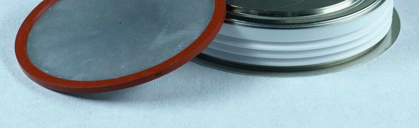
ABB Switzerland Ltd.

Large Area Fast Recovery Diode with Very High SOA Capability for
IGCT Applications
J. Vobecký, R. Siegrist, M. Arnold, K. Tugan
ABB Switzerland Ltd, Semiconductors, Fabrikstrasse 3, CH - 5600 Lenzburg, Switzerland
jan.vobecky@ch.abb.com

The Power Point Presentation will be available after the conference.

Abstract
A large area (>50 cm 2) fast recovery 4.5 kV silicon diode with very low leakage current and high SOA
up to 140 oC was developed for IGCT applications. The silicon design and lifetime control has also
been optimized for soft reverse recovery and high cosmic ray withstanding capability of 100 FIT at
2.8 kV. Furthermore, a defect peak of ion irradiation shielded from the reverse bias space charge re-
gion by anode buffer combined with electron irradiation were used for shaping the ON-state plasma
and reduction of reverse recovery losses. In addition to low leakage currents, the new design provides
a strong anode for high ruggedness during reverse recovery without a di/dt choke up to 10 kA/ s. The
diode parameters are compared for low- and high-energy electron irradiations in terms of leakage cur-
rent, temperature coefficient of the forward voltage drop, technology curve VF vs. Erec, softness of re-
verse recovery and surge current.

1.      Introduction
High SOA IGCTs for state-of-the-art voltage source inverters have increased their current handling
capability from around 3.5kA to over 5 kA at a 2.8 kV dc link voltage [1]. Since the IGCT have the po-
tential to operate above 125 oC, the complementary free wheeling and neutral point clamping diodes
have to follow this trend, if placed into a common stack. This requires to turn-off higher currents at the
same di/dt and dc link voltage, and at higher temperatures. The placement of a diode into the com-
mon stack with IGCTs requires also the same package size with 85 mm pole piece. The size of the
accompanying diodes can be then close to 4” ( 50 cm2) and the fast recovery diode design has to
cope with very large area scaling.
By increasing the size of a diode, the following parameters can be improved:
The forward voltage drop VF, the thermal resistance Rth, the reverse bias safe operation area RBSOA
(lower dynamic avalanche), the forward bias safe operation area FBSOA (lower forward recovery
voltage Vfr and higher surge current).
Nevertheless, by increasing the size of a diode, the following parameters will be adversely affected:
The leakage current, the temperature coefficient of forward voltage drop VF, the reverse recovery
losses Erec, charge Qrr, and softness.

                       Fig. 1. Large area fast recovery diode with 85 mm pole piece.

PCIM                                             Page 1 of 7                               Nuremberg 2011
ABB Switzerland Ltd.

In this paper we present the physical principles and design features one has to apply in order to cope
with the deterioration of the electrical parameters when the diode area is increased significantly. By
doing so, the electrical behaviour of the 4.5 kV fast recovery diode is shown to satisfy the needs of
high-power IGCTs up to 140 oC.

2.      Device parameters

2.1.    Leakage Current
Fig.2 (left) shows the results from high-temperature reverse bias test (HTRB), in which a diode is bi-
ased at 3.6 kV at elevated temperature. The leakage current was registered for every 5 oC after sev-
eral hours in order to determine, whether thermal run-away takes place (see failure point in red). The
graph shows that for the free-floating silicon configuration employed with a diode area above 50 cm 2,
the safe operation at a given temperature requires that the leakage current is not higher than 50 mA.

Fig. 2. Leakage current vs. junction temperature (left). Local lifetime control concept at anode (right).

Fast recovery P-i-N diodes require an intensive recombination lifetime control in order to reduce the
reverse recovery losses Erec and achieve high RBSOA capability. As a result, relatively high concen-
trations of deep levels are introduced into the silicon bulk with subsequent reductions of recombina-
tion lifetime levels and increased leakage currents. The impact of deep levels placed in the space
charge region (SCR) of a reverse biased diode on leakage current is given by eq. (1)
                                              SCR
                                                          en e p
                                    I   A e         NT                 , (1)
                                               0
                                                         en       ep
where A is the diode area, e is the electron charge, NT the concentration of deep levels and en and ep
are the emission rates of electrons and holes, respectively. This means that the deep levels without
any impact on the leakage current are the ones outside the SCR. Such levels are used for the local
lifetime control of anode regions by ion irradiation in order to reduce reverse recovery peak power
and voltage oscillations. This is due to the fact that they are shielded from the electric field by the an-
ode buffer shown in Fig.2 (right). Practically, only the tail of the SCR is allowed to reach the peak de-
fect region at the nominal breakdown voltage of 4.5 kV, so that the increase in leakage current after
ion irradiation is minimized.
On the other hand, for setting the recombination lifetime in the bulk, electron irradiation is employed.
In this case, the deep levels are placed in the whole SCR, and will therefore cause the dominant in-
crease of leakage current. The minimization of the leakage current will then require careful considera-
tion of the effective emission rates (en.ep)/(en+ep) in eq.(1)) of the deep levels created by the electron
irradiation. Since the annealing temperature after irradiation is below 300 oC, the dominant deep lev-
els are the single acceptor level of divacancy V-V (EC - 0.42 eV) and the acceptor level of vacancy-
oxygen pair V-O (EC - 0.16 eV). The divacancies, which control the lifetime at low-level injection,
causes much higher leakage currents than the V-O pairs, which control the high-level lifetime. This

PCIM                                                Page 2 of 7                             Nuremberg 2011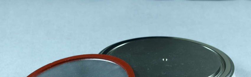
ABB Switzerland Ltd.

can be compensated by taking into account the fact that the production rate of the V-V relative to that
of the V-O decreases with decreasing irradiation energy [2, 3]. For lower energies of electron irradia-
tion, the leakage current is lower in spite of the fact that a higher irradiation dose is needed in order to
achieve the same reduction of recovery losses. This reflects in Fig.3, which compares the leakage
current vs. electron irradiation dose for Low- (LEE) and High-Energy Electron irradiation (HEE) in the
range of doses resulting in similar recovery losses. Thanks to a twofold reduction of the leakage cur-
rent after the LEE compared to that of the HEE one, the diode with LEE can safely operate at 140 oC
(see Fig.2).

 Fig. 3. Leakage current vs. electron irradiation        Fig. 4. Forward I-V curves of combined ion
         dose for low- and high-energy electron ir-              and electron irradiated diodes
         radiations.                                             measured at 25 and 125 oC for different
                                                                 areas A and thicknesses t .

2.2.    Temperature Coefficient of Forward Voltage Drop VF
The purpose of increasing the diode area is to decrease the forward voltage drop VF. The dominant
portion of VF is that of the thick electron irradiated low-doped n-base, where mobility and lifetime
are the dominant temperature dependent components according to the following formula [4, 5]
                                                  1
                                 Vbase                           .      2
                                            T,n        T,n
While (T, n) always monotonously decreases with increasing temperature and carrier concentration,
 (T, n) can increase or decrease with increasing temperature and carrier concentration according to
the specific behaviour of the introduced deep levels. The mutual behaviour of the functions (T, n)
and (T, n) determines the point at which the low temperature forward I-V curve crosses the high tem-
perature curve. Below and above the crossing point, the temperature coefficient of the forward volt-
age drop VF is negative and positive, respectively. In principal, the crossing point current is at higher
level with increasing n-base thicknesses t and larger areas A (see Fig.4). Note that the increase of the
crossing point with increasing thickness is much stronger in the large area diode. In these diodes, the
crossing point is already very high before irradiation as is illustrated in Fig.5. After ion irradiation into
the anode buffer, the crossing point decreases, and subsequently becoming higher again after the
electron irradiation.
On one hand, the (T, n) decreases with increasing temperature independently of deep levels in the
range of applied irradiation doses. On the other hand, the (T, n) rises more strongly with increasing
temperature when a higher concentration of shallower deep levels (e.g. V-O instead of V-V) is pre-
sent. This occurs for example when diodes are annealed above 300 oC or when the energy of electron
irradiation is decreased from the HEE level to that of LEE. Higher concentrations of shallower (lower
leakage current) levels will then result in the temperature coefficient VF becoming more negative, i.e.
it takes up the crossing point current to higher currents. At high doses of the LEE, the crossing point
disappears as is shown in Fig.5 (right), which is drawn for the HEE and LEE devices with equal re-

PCIM                                              Page 3 of 7                                 Nuremberg 2011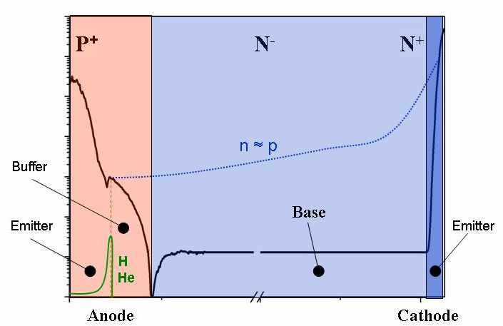
ABB Switzerland Ltd.

verse recovery losses. This means that the large area devices subjected to the LEE, which have very
low leakage currents up to higher temperatures, are not suitable for paralleling. On the other hand,
this issue is not a problem of low area diodes, such as in the case of chip diodes with A 1 cm2,
which have in principle a low crossing point current level.

Fig. 5. Forward I-V curves of unirradiated, ion irradiated and combined ion and HEE diodes of the
        same area A = 53 cm2 (left). Forward I-V curves of combined ion and electron irradiated di-
        odes with different energies of electron irradiation, namely HEE and LEE (right).

2.3.    Reverse recovery
The diode for high power IGCT applications has to withstand the currents levels above 6 kA with sub-
sequent turn-off at a 2.8 kV dc link voltage. In addition, at the same dc link voltage, the diode has to
safely turn-off at current densities well below 1 A/cm 2. Since the guarantee of cosmic ray withstanding
capability of 100 FIT at 2.8 kV dictates the usage of the starting silicon specification with a relatively
high resistivity, excessive demands are laid on the design for soft recovery. For this purpose, the life-
time control and n-base thickness had to be optimized at the same time.

 Fig. 6. Technology curve of combined ion and          Fig. 7. Voltage overshoot vs. current density.
         HEE vs. LEE irradiated diodes. Leakage                Bottom: devices highlighted by dashed
         current measured at 4.5 kV @ 140 oC is                rectangle in Fig.5. Top: thinner devices
         labeled for every group.                              with softer behavior of LEE ones.

The ion irradiation into the anode buffer (Fig.2 right) is a very efficient mean for making the diode re-
covery softer without decreasing SOA and with only a very little increase in VF. To suppress the dy-
namic avalanche and reduce the reverse recovery loss Erec, the electron irradiation is used. The low-
energy electron irradiation gives a slightly worse technology curve (see Fig.6), but then it also pro-

PCIM                                            Page 4 of 7                                Nuremberg 2011
ABB Switzerland Ltd.
vides much lower leakage currents and improved softness, especially if thinner devices are used. This
is due to the fact that low energy irradiation controls the carrier lifetime locally and leaves more ex-
cess carriers prior to turn-off at the cathode side. Fig.7 shows the peak anode voltage (voltage over-
shoot) versus the anode current density. For the dc link voltage of 2.8 kV at high current densities,
overshoot voltages are observed between 3.4 and 3.5 kV (see Fig.8), which are given by the clamp-
ing diode circuit. In addition, we have additional overshoots caused by the snap-off of the diode cur-
rent at lower current densities, which cause unwanted oscillations of voltage and current. For the de-
vices from Fig.7 (top) they take place below 5 A/cm 2 and from Fig.7 (bottom) below 1.5 A/cm 2.
Although the thicker n-base increases VF, it can provide improved softness with less lifetime killing.
For the same softness, the Vf of a thicker device can be then lower than that of the thinner one. In
such a case, both the HEE and LEE give similar softness as shown in Fig.7 (bottom) for the devices
depicted by the dashed line in the Fig.6. Fig.7 represents the worst case in terms of di/dt and temper-
ature. Below 100 oC and towards higher di/dts the oscillations start only below 0.5 A/cm 2 at 2.8 kV dc
voltage.
3. Device performance
Using the design principles mentioned above, diodes were processed on 4-inch silicon wafers and cut
to the diameter of 91 mm. The leakage current was obtained below 40 mA at 140 oC thus giving suffi-
cient margin for reliable operation, if any short-term temperature excursion above this limit occurs.
The forward voltage drop is that of the technology curve in Fig.6. The diode has a rectangular single-
pulse SOA of 3.2 kV and 7 kA up to 140 oC and di/dt 1.5 kA/ s (see Fig.8 left). The measurements
above 7 kA were not performed due to the limitation of current source.
Fig. 8. Reverse recovery at 2.8 kV from IF = 7 kA at 140 oC. (left). SOA under reverse recovery with
di/dt 8 -10 kA/ s limited only by IGCT and LS vs. dc link voltage with diode area as a pa-
rameter (right).
The prominent advantage of a large diode area is the very high maximal turn-off current during re-
verse recovery without a di/dt choke, when the di/dt grows with an increasing forward current towards
10 kA/ s. Fig.8 (right) shows this capability versus diode area and dc link voltage. All the diodes have
the same doping profiles and differ only in the size of the active area. Since the diode presented in
this paper has the largest area A 53 cm2, it achieves the last pass turn-off current above 1.5 kA at
2.8 – 3.0 kV dc link voltage.
The fact that the temperature coeffcient VF of large area diodes is negative up to high current levels
(see Fig. 5) might become an issue since large-area devices could have problems under surge cur-
rent conditions due to a stronger current localization. The counter-clockwise rotation of the I-V locus
supports this assumption (see Fig.9 left), especially because it was also measured for devices with
crossing point current levels down to 2.5 kA. However, Fig.9 right shows the value of the last pass
surge current to be independent of the irradiation technology used and strongly correlating with the
PCIM Page 5 of 7 Nuremberg 2011ABB Switzerland Ltd.
value of VF. This means that the surge current capability is driven by the overall power losses (heat)
generated during overloading and not by the temperature coefficient VF. More detailed explanation of
this feature was provided by a visual inspection of the wear-out pattern of aluminium metallization
when approaching the failure current. The investigation shows that the surge current is evenly distrib-
uted along the whole device perimeter at its inner side. The localisation of current takes place only
during failure and always in the bulk. A straightforward way to increase the maximal surge current I FSM
in a diode is therefore to decrease the VF. The increase of device thickness while keeping the same or
even lower VF would bring an additional improvement as illustrated in Fig.9.
Fig. 9. I-V locus of HEE and LEE devices with equal VF measured with a half-sine pulse width
tp = 16 ms at 125 oC during failure (left) Last pass surge current vs. forward voltage drop VF
for LEE and HEE devices with different thicknesses and irradiation doses (right).
4. Conclusions
A new large area fast recovery diode with low leakage currents, soft recovery behaviour, high current
handling capability and cosmic ray withstanding capability of 100 FIT at 2.8 kV was presented. The
improved performance will enable the diode to operate in a common stack with high SOA IGCTs with-
out compromising the operating temperature. Common scaling design challenges of large area silicon
diodes, such as excessive leakage current levels and limited softness of reverse recovery, have been
overcome by using optimized carrier lifetime control and device dimensions. The RBSOA with con-
stant di/dt in the range between 0.5 and 1.5 kA/ s is rectangular up to 7 kA and 3.2 kV @ 140 oC. In
addition, the strong diode anode profile in terms of injection efficiency and sufficient softness during
reverse recovery provides the rectangular RBSOA with di/dt capabilities up to 10 kA/ s up to
o
1.5 kA @ 3.0 kV @ 125 C.
5. References
[1] T. Wikstrom, T. Stiasny, M. Rahimo, D. Cottet, P. Streit, "The Corrugated P-Base IGCT – a New
Benchmark for Large Area SOA Scaling", Proc. ISPSD´07, Korea, pp. 29-32, 2007.
[2] Y. Morikawa, T. Miura, M. Kekura, S. Miyazaki, F. Ichikawa, „Sloping Lifetime Control by Electron
Irradiation for 4.5 kV PT-SIThs“ Proceedings of the ISPSD 97, 1997, p. 61, 1997.
[3] P. Hazdra, J. Vobecky, H. Dorschner, K. Brand, „Axial Lifetime Control in Silicon Power Diodes by
Irradiation with Protons, Alphas, Low- and High-Energy Electrons“, Microelectronics Journal 35, pp.
249 - 257, 2004
[4] J. Vobecky, P. Hazdra, O. Humbel, N. Galster, ”Crossing Point Curent of Electron and Proton Irra-
diated Power P-i-N Diodes”, Microelectronics Reliability 40, pp. 427 – 433, 2000.
PCIM Page 6 of 7 Nuremberg 2011ABB Switzerland Ltd. [5] J. Vobecky, P. Hazdra, V. Zahlava, "Impact of the Electron, Proton and Helium Irradiation on the Forward I-V Characteristics of High-Power P-i-N Diode", Microelectronics Reliability 43, pp. 537 – 544, 2003. PCIM Page 7 of 7 Nuremberg 2011
You can also read