User Manual Demo Kit for the Smart Bus Converter Test-Chip D2852
←
→
Page content transcription
If your browser does not render page correctly, please read the page content below
User Manual
         Demo Kit for the Smart Bus
         Converter Test-Chip D2852
                                       UM-PM-60

Abstract
This user manual describes how to connect and use the D2852 test chip. The D2852 introduces
Dialog's ground breaking HyPer Converter technology and the corresponding upcoming smart bus
converter product DA9513.

Disclaimer:

This Demo-Kit is manufactured without final inspection. It is using ICs that has NOT been checked in
production. By that your sample may not work as described in the appendix. In this case please
contact the Dialog Semiconductor customer support for replacement. The test chip implements only
limited protection features and contains a wrong setting in the control logic and by that may be
destroyed during certain test cases. So please read the user manual carefully BEFORE applying
power to your Demo-Kit!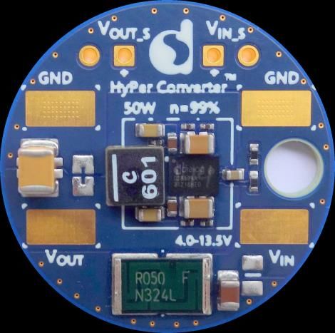
UM-PM-60
Demo-Kit of Test-Chip D2852

Contents
Abstract ................................................................................................................................................ 1
Contents ............................................................................................................................................... 2
Figures .................................................................................................................................................. 2
Tables ................................................................................................................................................... 2
1    Terms and Definitions ................................................................................................................... 3
2    References ..................................................................................................................................... 3
3    Introduction.................................................................................................................................... 4
4    Input/Output Connections ............................................................................................................ 4
5    Operating Instructions .................................................................................................................. 5
     5.1 Connect a DC Power Supply ................................................................................................ 5
     5.2 Connect the Load .................................................................................................................. 5
     5.3 Turn On the Input Power Supply ........................................................................................... 5
     5.4 Turn On the Electronic Load ................................................................................................. 5
     5.5 Turn Off the Electronic Load ................................................................................................. 5
     5.6 Shut Down the Converter ...................................................................................................... 6
6    Conclusions ................................................................................................................................... 6
Appendix A - Demo-Kit D2852 Typical Performance ....................................................................... 7
   A.1 Electrical Characteristics ....................................................................................................... 7
   A.2 Efficiency ............................................................................................................................... 7
   A.3 Transient Load Response ..................................................................................................... 9
Appendix B - BOM Customisation ................................................................................................... 10

Figures
Figure 1: D2852 Input/Output Connections ........................................................................................... 4
Figure 2: Demo-Kit Dimensions on Scale ............................................................................................. 6
Figure 3: Converter Efficiency @ VIN = 6V ............................................................................................ 7
Figure 4: Converter Efficiency @ VIN = 9V ............................................................................................ 8
Figure 5: Converter Efficiency @ VIN = 12V .......................................................................................... 8
Figure 6: Transient Load Response @ VIN = 7.6V (CBUS = 100uF) ....................................................... 9
Figure 7: D2852 BOM Customisations ................................................................................................ 10

Tables
Table 1: Electrical Characteristics ......................................................................................................... 7

User Manual                                                       Revision 1.0

CFR0012                                                                 2 of 11                                          © 2021 Dialog Semiconductor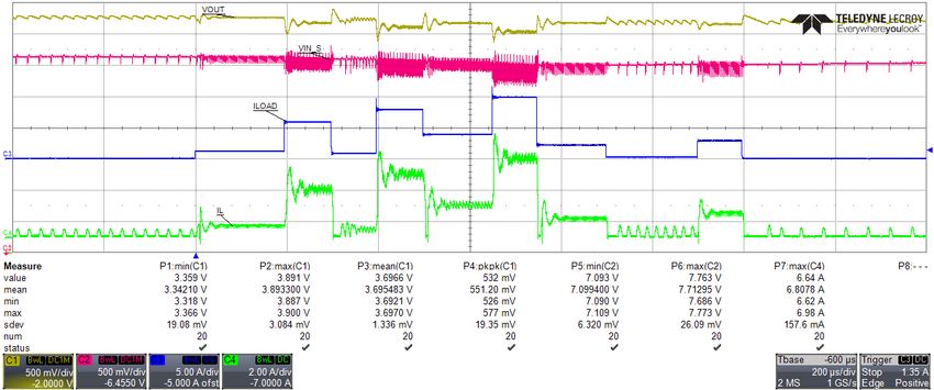
UM-PM-60
Demo-Kit of Test-Chip D2852

1      Terms and Definitions
2S                 Battery Pack with 2x (Li-Ion) Cells connected in series
3S                 Battery Pack with 3x (Li-Ion) Cells connected in series
BOM                Bill Of Material
CCM                Continuous Conduction Mode
DCM                Discontinuous Conduction Mode
DC-DC              Direct Current to Direct Current Converter
FET                Field Effect Transistor
IC                 Integrated Circuit
Li-Ion             Lithium-Ion
OTP                One Time Programmable Memory
PCB                Printed Circuit Board
PFM                Pulse Frequency Mode

2      References
[1]   D2852 Databrief, Rev. 1.0, Dialog Semiconductor, 2021
[2]   D2852 Welcome Note, Dialog Semiconductor, 2021

User Manual                                Revision 1.0

CFR0012                                        3 of 11                       © 2021 Dialog Semiconductor
UM-PM-60
Demo-Kit of Test-Chip D2852
3 Introduction
Dialog Semiconductor (now part of Renesas Electronics Corporation) is introducing a new family of
patent protected Hybrid Power-efficient regulating Converters, subsequently called
HyPer ConverterTM.
For the provision of regulated output power @ conversion efficiency up to 99% the
HyPer ConverterTM combines switched-capacitor and inductive conversion within a single DC-DC
topology. The D2852 is the first test chip in this family of converters. It is an easy to use smart
intermediate bus converter that supports input voltages between 4V and 13.5V and produces varying
output voltages between 2.8V to 5V, effectively implementing a battery pack de-serializer. Across
multiple decades of load current the D2852 delivers the maximum energy from multi-cell battery
packs, thus make the upcoming product chip most suitable for 2S & 3S battery powered applications.
It converts up to 50W of peak power, offers fully integrated power switches and requires only small
and low-profile external components, allowing minimum PCB footprint implementation in compact
applications.
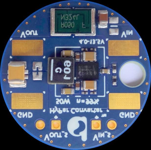
4 Input/Output Connections
Figure 1 shows the input/output connections of the D2852 Demo-Kit.
Kelvin Connection of Kelvin Connection of
Output Voltage Input Voltage
External Load Connection to
Output Power Supply
Figure 1: D2852 Input/Output Connections
Please ensure correct polarity (see pad labels printed to the board). The wires soldered to the pads
for the supply and the external load need to be capable of handling the target currents ( 1.5mm).
The wires need to soldered carefully, so that other PCB components are not lifted or shorted.
User Manual Revision 1.0
CFR0012 4 of 11 © 2021 Dialog SemiconductorUM-PM-60 Demo-Kit of Test-Chip D2852 5 Operating Instructions 5.1 Connect a DC Power Supply The power supply should be set for a minimum output voltage of 4V and a maximum output voltage of 13.5V and capable of supplying up to 20A (ensure good margin to the target peak load power). 5.2 Connect the Load The load should be capable of handling the target load current range with some margin (10A peak). 5.3 Turn On the Input Power Supply The Demo-Kit automatically powers up as soon it detects a valid supply voltage in the range of 4V – 13.5V. For the start-up configure the power supply to a voltage larger than 6V. At this point no load should be applied to the Demo-Kit (the upcoming product DA9513 will support start-up load currents up to 2A). The smart bus converter selects for any applied input voltage automatically the output voltage with optimum converter efficiency (in the range of 2.8V to 5V). The varying output voltage is applied in steps of ~60mV. Ripple in the supply voltage and certain load currents may trigger an alternation of the output voltage between adjacent steps. The smart bus converter supervises output voltage and efficiency and continuously optimizes the DC-DC switching sequence for optimum performance. 5.4 Turn On the Electronic Load As soon as the output voltage has fully ramped up, load current may be applied. The maximum continuous load current is 8A, with peaks up to 10A. After applying load current the supply voltage may be adjusted to a different level (within 4V and 13.5V). IMPORTANT ADVICE As it may trigger damage do not actively pull the input voltage DOWN, in particular when there is no load connected on the output. Instead, make sure to apply a minimum load current of 2A when reducing the input voltage quickly! Because of a wrong logic setting in the test chip it is generally not recommended to test fast line transients. As short voltage drops at the converter input may trigger the activation of the embedded Under- Voltage protection special care must be taken during high load currents applied at low supply voltages and when ramping up the supply voltage from its minimum level. In the same way spikes in the supply voltages higher than 13.5V may trigger the Over-Voltage protection followed by an immediate shut-down of converter operation. This shut-down is uncritical in combination with natural and electronic loads (that stop pulling current as soon as the output voltage reaches zero). Do not use source-meters that may actively drive the output towards negative voltages as this may harm the DC-DC converter (especially during shut-down at high load currents). To become less dependent on the power supply and instead emulate a battery pack at the input a large decoupling cap (several mF) may be used. The Demo-Kit includes a power resistor for converter evaluation with non-ideal sources (emulation of 50mΩ battery pack impedance). At high load currents this source impedance is furthermore heating- up the small PCB to emulate typical application temperature rise from sinks dissipating the converter output power. With that the tiny Demo-Kit implements a more realistic performance than conventional evaluation boards. Please note that a third protection mechanism terminates converter operation if overloading the Demo-Kit for a longer duration (towards excessive junction temperature). For efficiency estimations Kelvin connected pads are provided at the top of the PCB, enabling accurate measurements of converter input and output voltage. For the evaluation of transient load responses it is recommended to connect a large bulk capacitor (>20mF) to the power supply pads. 5.5 Turn Off the Electronic Load Decrease the load current to zero and then turn off the load. User Manual Revision 1.0 CFR0012 5 of 11 © 2021 Dialog Semiconductor
UM-PM-60
Demo-Kit of Test-Chip D2852

5.6       Shut Down the Converter
Turn off the Power Supply after disabling load current. In case the converter has been disabled by an
embedded protection circuit the supply voltage needs to reach zero for converter reset.
Note 1    For converter reset ensure that input capacitance is fully discharged (VIN_S < 2V)

6        Conclusions
This Demo-Kit of the D2852 test chip introduces the industry leading combination of power density
and efficiency from Dialog’s new family of smart HyPer ConvertersTM:

                                Figure 2: Demo-Kit Dimensions on Scale

To enable customer access as soon as possible the Demo-Kit has been manufactured with the first
test ICs, so that some care is required during operation. The ICs and the boards have not received
any final production checks, so that your sample may not implement the typical performance as
presented in the appendix. In this case please contact the Dialog Semiconductor Customer Support
for replacement.

We would be more than happy to receive feedback from your first hand experience. And if you like it,
you are welcome to always have this Demo-Kit with you as your new Limited Edition Key-Fob…

User Manual                                     Revision 1.0

CFR0012                                             6 of 11                              © 2021 Dialog Semiconductor
UM-PM-60
Demo-Kit of Test-Chip D2852
Appendix A - Demo-Kit D2852 Typical Performance
A.1 Electrical Characteristics
Table 1: Electrical Characteristics
Symbol Parameter Test Conditions Min Typ Max Unit
VDD Input Voltage 4 13.5 V
VOUT Output Voltage 2.8 5.5 V
COUT Output Capacitance Including Derating 60 F
IOUT_MAX Max. Output Current 8 A
IOUT_PEAK Peak Output Current Pulses of < 20ms duration
10 A
@ duty cycle < 30%
fSW Nominal Converter Fixed frequency mode
520 570 630 kHz
Switching Frequency
ηPEAK Peak Efficiency 1x 47uF 0805 per phase, VDD = 9V,
99.0 %
IOUT = 1A
ηCCM High Current Efficiency 1x 47uF 0805 per phase, VDD = 9V,
97.8 %
IOUT = 5A
ηPFM Light Load Efficiency 1x 47uF 0805 per phase, VDD = 9V,
98.5 %
IOUT = 10 – 1000mA
Note 2 Inductor Coilcraft XGL4020-601
A.2 Efficiency
VIN = 6V (CF = 47uF, L = XGL4020-601)
100,0
99,0
98,0
97,0
Efficiency [%]
96,0
95,0
94,0
93,0
92,0
91,0
90,0
0,01 0,1 IOUT [A] 1 10
Figure 3: Converter Efficiency @ VIN = 6V
User Manual Revision 1.0
CFR0012 7 of 11 © 2021 Dialog SemiconductorUM-PM-60
Demo-Kit of Test-Chip D2852
VIN = 9V (CF = 47uF, L = XGL4020-601)
100,0
99,0
98,0
97,0
Efficiency [%]
96,0
95,0
94,0
93,0
92,0
91,0
90,0
0,01 0,1 IOUT [A] 1 10
Figure 4: Converter Efficiency @ VIN = 9V
VIN = 12V (CF = 47uF, L = XGL4020-601)
100,0
99,0
98,0
97,0
Efficiency [%]
96,0
95,0
94,0
93,0
92,0
91,0
90,0
0,01 0,1 IOUT [A] 1 10
Figure 5: Converter Efficiency @ VIN = 12V
Note 3 At load currents < 2.5A the DC-DC Converter may operate in either CCM or PFM (automatically
selected depending on the load current and slewing direction). The above plots show the higher value
of the corresponding efficiency results.
Note 4 Efficiency may be further improved via additional flying capacitors
User Manual Revision 1.0
CFR0012 8 of 11 © 2021 Dialog SemiconductorUM-PM-60
Demo-Kit of Test-Chip D2852
A.3 Transient Load Response
Figure 6: Transient Load Response @ VIN = 7.6V (CBUS = 100uF)
Note 5 ILOAD Start = 100mA, ILOAD (duration) = 1.3A (200us), 6A (100us), 0.9A (100us), 8A (100us), 4A
(150us), 10A (100us), 2.3A (150us), 0.3A (200us), 3A (100us), 0.1A (100us)
User Manual Revision 1.0
CFR0012 9 of 11 © 2021 Dialog SemiconductorUM-PM-60
Demo-Kit of Test-Chip D2852
Appendix B - BOM Customisation
Combi-Pad for
alternative inductors
Flying capacitors
Combi-Pads for
alternative/additional
output capacitance
Space for additional
input capacitance
Figure 7: D2852 BOM Customisations
This revision of the Demo-Kit has been manufactured with the inductor XGL4020-601 (offering
current ratings sufficient for DC-DC converter load up to 10A). This is a deviation against the 470nH
standard inductance of the D2852 and caused by the world-wide component shortage. Applications
with reduced current demand may be evaluated with alternative 470nH inductors of reduced current
rating and footprint. A Combi-Pad is prepared to enable the replacement of the populated inductor
with inductors down to 2.5x2.0mm or even 2.0x1.6mm footprint. Furthermore the converter
performance may be checked with additional input and output capacitance. The flying and the output
bus capacitors are soldered to Combi-Pads so that the populated components may be replaced with
capacitors of e.g smaller footprint. Please note that larger changes of BOM parameters require ICs
with changed converter settings, which can only be implemented by the Dialog Application
Engineering.
User Manual Revision 1.0
CFR0012 10 of 11 © 2021 Dialog SemiconductorUM-PM-60 Demo-Kit of Test-Chip D2852 Disclaimer Unless otherwise agreed in writing, the Dialog Semiconductor products (and any associated software) referred to in this document are not designed, authorized or warranted to be suitable for use in life support, life-critical or safety-critical systems or equipment, nor in applications where failure or malfunction of a Dialog Semiconductor product (or associated software) can reasonably be expected to result in personal injury, death or severe property or environmental damage. Dialog Semiconductor and its suppliers accept no liability for inclusion and/or use of Dialog Semiconductor products (and any associated software) in such equipment or applications and therefore such inclusion and/or use is at the customer’s own risk. Information in this document is believed to be accurate and reliable. However, Dialog Semiconductor does not give any representations or warranties, express or implied, as to the accuracy or completeness of such information. Dialog Semiconductor furthermore takes no responsibility whatsoever for the content in this document if provided by any information source outside of Dialog Semiconductor. Dialog Semiconductor reserves the right to change without notice the information published in this document, including, without limitation, the specification and the design of the related semiconductor products, software and applications. Notwithstanding the foregoing, for any automotive grade version of the device, Dialog Semiconductor reserves the right to change the information published in this document, including, without limitation, the specification and the design of the related semiconductor products, software and applications, in accordance with its standard automotive change notification process. Applications, software, and semiconductor products described in this document are for illustrative purposes only. Dialog Semiconductor makes no representation or warranty that such applications, software and semiconductor products will be suitable for the specified use without further testing or modification. Unless otherwise agreed in writing, such testing or modification is the sole responsibility of the customer and Dialog Semiconductor excludes all liability in this respect. Nothing in this document may be construed as a license for customer to use the Dialog Semiconductor products, software and applications referred to in this document. Such license must be separately sought by customer with Dialog Semiconductor. All use of Dialog Semiconductor products, software and applications referred to in this document is subject to Dialog Semiconductor’s Standard Terms and Conditions of Sale, available on the company website (www.dialog-semiconductor.com) unless otherwise stated. Dialog, Dialog Semiconductor and the Dialog logo are trademarks of Dialog Semiconductor Plc or its subsidiaries. All other product or service names and marks are the property of their respective owners. © 2021 Dialog Semiconductor. All rights reserved. RoHS Compliance Dialog Semiconductor’s suppliers certify that its products are in compliance with the requirements of Directive 2011/65/EU of the European Parliament on the restriction of the use of certain hazardous substances in electrical and electronic equipment. RoHS certificates from our suppliers are available on request. Contact Dialog Semiconductor General Enquiry: Local Offices: Enquiry Form https://www.dialog-semiconductor.com/contact/sales-offices User Manual Revision 1.0 CFR0012 11 of 11 © 2021 Dialog Semiconductor
You can also read