LIBERO SOC V2021.2 - MICROSEMI
←
→
Page content transcription
If your browser does not render page correctly, please read the page content below
Libero® SoC v2021.2
                       PolarFire® SoC MSS Simulation User Guide

Introduction
The PolarFire SoC Microcontroller Subsystem (MSS) is modeled with Microchip AMBA Bus Functional Model (BFM)
to support functional simulation.
Note:
For information on supported instructions and the BFM commands syntax, see DirectCore Advanced Microcontroller
Bus Architecture - Bus Functional Model User's Guide.
The MSS BFM based simulation model provides a simulation environment for the PolarFire SoC FPGA fabric logic,
typically replacing the MSS system block in a design. Simulation can be useful in the following applications:
  •   Verifying the connectivity with the FPGA fabric logic.
  •   Addressing peripherals, memories etc. in the FPGA fabric that are connected to the MSS using the Fabric
      Interface Controllers (FICs).
  •   Accessing MSS-DDR from FPGA fabric master using FICs.
  •   Accessing the Crypto from FPGA fabric through AHB and streaming interface.
  •   Generation of H2F and F2H interrupts.

© 2021 Microchip Technology Inc.                        User Guide                              DS50003088C-page 1
and its subsidiaries
Libero® SoC v2021.2 Figure 1. MSS Simulation Model Architecture © 2021 Microchip Technology Inc. User Guide DS50003088C-page 2 and its subsidiaries
Libero® SoC v2021.2

Table of Contents
Introduction.....................................................................................................................................................1

1.    Creating a new PolarFire SoC Project.................................................................................................... 4

2.    Simulation Flow.......................................................................................................................................5
      2.1.       FIC Interface.................................................................................................................................5
      2.2.       Interrupts.................................................................................................................................... 10
      2.3.       User Cryptoprocessor................................................................................................................ 14
      2.4.       DDR Controller........................................................................................................................... 21
      2.5.       QoS Parameter.......................................................................................................................... 25

3.    Revision History.................................................................................................................................... 28

4.    Microchip FPGA Technical Support...................................................................................................... 29
      4.1.       Customer Service.......................................................................................................................29
      4.2.       Customer Technical Support...................................................................................................... 29
      4.3.       Website...................................................................................................................................... 29
      4.4.       Outside the U.S.......................................................................................................................... 29

The Microchip Website.................................................................................................................................30

Product Change Notification Service............................................................................................................30

Customer Support........................................................................................................................................ 30

Microchip Devices Code Protection Feature................................................................................................ 30

Legal Notice................................................................................................................................................. 31

Trademarks.................................................................................................................................................. 31

Quality Management System....................................................................................................................... 32

Worldwide Sales and Service.......................................................................................................................33

© 2021 Microchip Technology Inc.                                                     User Guide                                                      DS50003088C-page 3
and its subsidiaries
Libero® SoC v2021.2
Creating a new PolarFire SoC Project
1. Creating a new PolarFire SoC Project
Use the MSS standalone configurator tool and Libero® SoC to create MSS-based designs. For more information, see
the MSS Standalone Configurator User Guide.
1. Create the MSS configurator using the pfsoc_mss application by either creating a new configuration (.cfg)
file or by opening an existing one.
2. Configure the MSS subsystem with the required FIC interface and other necessary modules like DDR and
Crypto.
3. Generate the MSS component file (.cxz).
After finishing with the MSS standalone configuration, import the MSS subsystem into Libero, and then design the
entire system, as follows:
1. Open the Libero SoC Design Suite.
2. Create the project.
3. Invoke system builder to create your MSS block.
4. Import the MSS component file.
5. Design your entire system using MSS, AXI4 interconnect, fabric slaves, and fabric masters.
6. After designing the entire system, check the DRC and generate the system.
7. Add supported BFM instructions in the BFM files created in project.
8. Add required test bench to perform simulation.
9. Launch the Pre-Synth simulation.
Figure 1-1. Launching Simulation
© 2021 Microchip Technology Inc. User Guide DS50003088C-page 4
and its subsidiariesLibero® SoC v2021.2
Simulation Flow
2. Simulation Flow
2.1 FIC Interface
The PolarFire SoC FPGA provides multiple FICs to enable connectivity between user logic in the FPGA fabric and
the MSS. FIC is part of the MSS and acts as a bridge between the MSS and the FPGA fabric. The master FIC
interface provides access to the address range listed in the following table.
Table 2-1. FIC Interface Address Ranges
FIC Interface Number of Regions Start Address End Address Size
FIC0 2 0x6000_0000 0x7FFF_FFFF 512 MB
0x20_0000_0000 0x2F_FFFF_FFFF 64 GB
FIC1 2 0xE000_0000 0xFFFF_FFFF 512 MB
0x30_0000_0000 0x3F_FFFF_FFFF 64 GB
FIC3 1 0x4000_0000 0x5FFF_FFFF 512 MB
The master FIC allows and initiates the AXI transaction only when addresses entered in the BFM file are within the
dedicated address range. Otherwise, it shows a DRC in the simulation log.
The slave FIC responds to AXI master in fabric in the following way:
• Uses AXI transaction details to clear interrupts and provides a valid AXI response.
• Provides a transparent connection between the AXI switch and FIC interface to access the DDR controller and
DDR memory.
• Prints a message in the simulation log in case of incorrect addressing for other addresses.
2.1.1 BFM Commands
Libero generates BFM files for FIC interfaces as shown in the following table.
Table 2-2. FIC Interface Address Ranges
Module BFM file name
FIC0 PFSOC_MSS_FIC0
FIC1 PFSOC_MSS_FIC1
FIC3 PFSOC_MSS_FIC3
FIC4 PFSOC_MSS_FIC4
Note: PFSOC_MSS_FIC4 BFM will be created for only
S devices.
The following figure shows the BFM files that can be accessed from within the simulation folder in the Libero tool.
© 2021 Microchip Technology Inc. User Guide DS50003088C-page 5
and its subsidiariesLibero® SoC v2021.2
Simulation Flow
Figure 2-1. BFM Files in the Simulation Folder
All BFM commands specified in Microchip DirectCore AMBA BFM User's Guide and PolarFire PCI BFM and
SmartFusion2 FPGA High Speed Serial Interface Simulation can be used to simulate the MSS.
The following code block shows typical BFM instructions.
#===========================================================
# Enter your BFM commands in this file.
#
# Syntax:
# -------
#
# memmap resource_name base_address;
#
# write width resource_name byte_offset data;
# read width resource_name byte_offset;
# readcheck width resource_name byte_offset data;
#
#===========================================================
procedure main;
#FIC0 38bit Master Address declaration commands with memmap below
memmap FPR_BASE_ADDR_38bit 0x2060000000;
memmap FPR_BASE_ADDR_38bit_0 0x20600f0000;
memmap FPR_BASE_ADDR_38bit_1 0x20fffffff8;
#FIC0 32bit Master Address declaration commands with memmap below
memmap FPR_BASE_ADDR_int 0x60000000;
memmap FPR_BASE_ADDR_int_0 0x60003000;
memmap FPR_BASE_ADDR_int_1 0x60080000;
memmap FPR_BASE_ADDR_int_2 0x68000000;
#Array creation command below
int array[100];
#Creating table command below
table LEGALISATION 0x0000 0x0000 0x0000 0x0000 \
0x0000 0x0000 0xffff 0xffff \
0xffff 0xfffd 0xfe01 0xfff2 \
0xffff 0xfffd 0xfe05 0xffff
#Signal declaration command below
int u;
int l;
#Writing data command below
write64 w FPR_BASE_ADDR_38bit_1 0x8 0x32323232 0xaaaaaaaa
#Reading data command below
read64 w FPR_BASE_ADDR_38bit_1 0x8
#Reading and checking data command below
readcheck64 w FPR_BASE_ADDR_38bit_1 0x8 0x32323232 0xaaaaaaaa
#Writing data command below
write64 w FPR_BASE_ADDR_38bit 0x0 0x10102020 0xaaaaaaaa
#Writing data command below
© 2021 Microchip Technology Inc. User Guide DS50003088C-page 6
and its subsidiariesLibero® SoC v2021.2
Simulation Flow
write w 0x70000000 0x0 0x10102020
#Reading data command below
read w 0x70000000 0x0
#Reading and checking data command below
readcheck w 0x70000000 0x0 0x10102020
#Writing data command below
write h 0x70000000 0x32 0xdddd
#Reading data command below
read h 0x70000000 0x32
#Reading and checking data command below
readcheck h 0x70000000 0x32 0xdddd
#Writing data command below
write b 0x70000000 0x64 0xee
#Reading data command below
read b 0x70000000 0x64
#Reading and checking data command below
readcheck b 0x70000000 0x64 0xee
#Writing data command below
write w FPR_BASE_ADDR_int 0x0 0x10102020
#Reading data command below
read w FPR_BASE_ADDR_int 0x0
#Reading and checking data command below
readcheck w FPR_BASE_ADDR_int 0x0 0x10102020
#Reading data and store command below
readstore x FPR_BASE_ADDR_int 0x0 u
#Reading data and masking command below
readmask x FPR_BASE_ADDR_int 0x0 0x10102020 0xFFFFFFFF
#Writing burst data command below
writemult w FPR_BASE_ADDR_int_0 0x0 0xFFFFFFFF 0xEEEEEEEE 0xAAAAAAAA 0xBBBBBBBB
0xCCCCCCCC
#Reading burst data command below
readmult w FPR_BASE_ADDR_int_0 0x0 5
#Reading and checking burst data command below
readmultchk w FPR_BASE_ADDR_int_0 0x0 0xFFFFFFFF 0xEEEEEEEE 0xAAAAAAAA 0xBBBBBBBB
0xCCCCCCCC
#masking of poll data command below
pollmask w FPR_BASE_ADDR_int 0x0 0x10102020 0xFFFFFFFF
#position of pollbit command below
pollbit w FPR_BASE_ADDR_int 0x0 5 0x1
#craeting poll data command below
poll w FPR_BASE_ADDR_int 0x0 0x10102020
#filling data command below
fill w FPR_BASE_ADDR_int 0x40 3 0x00000000 0x0
#writing data to table command below
writetable w FPR_BASE_ADDR_int 0x100 LEGALISATION 4
#writing to array command below
writearray w FPR_BASE_ADDR_int 0x120 array[0] 1
#After filling check the data command below
fillcheck w FPR_BASE_ADDR_int 0x40 3 0x00000000 0x0
#reading table of data command below
readtable w FPR_BASE_ADDR_int 0x100 LEGALISATION 4
#reading array command below
readarray w FPR_BASE_ADDR_int 0x120 array[0] 1
#ahb cycle command below
ahbcycle w FPR_BASE_ADDR_int_1 0x0 0xBBBBBBBB 0x0
#memory testing command below
memtest FPR_BASE_ADDR_int_2 0x0 0x4 0x0 0x0 0x2
#Writing data command below
write64 w FPR_BASE_ADDR_38bit 0x0 0x10102020 0xaaaaaaaa
#Reading data command below
read64 w FPR_BASE_ADDR_38bit 0x0
#Reading and checking data command below
readcheck64 w FPR_BASE_ADDR_38bit 0x0 0x10102020 0xaaaaaaaa
#Reading data and store command below
readstore64 x FPR_BASE_ADDR_38bit 0x0 u l
#Display command below
print "Lower 32bits = %h", l
print "Upper 32bits = %h", u
© 2021 Microchip Technology Inc. User Guide DS50003088C-page 7
and its subsidiariesLibero® SoC v2021.2
Simulation Flow
#Reading data and masking command below
readmask64 x FPR_BASE_ADDR_38bit 0x0 0x10102020 0xaaaaaaaa 0xFFFFFFFF 0x0000FFFF
#Reading data and store command below
readstore64 x FPR_BASE_ADDR_38bit 0x0 u l
#Display command below
print "Lower 32bits = %h", l
print "Upper 32bits = %h", u
#Writing burst data command below
writemult64 w FPR_BASE_ADDR_38bit_0 0x0 0xFFFFFFFF 0xEEEEEEEE 0xAAAAAAAA 0xBBBBBBBB
0xCCCCCCCC 0xDDDDDDDD 0x01010101 0x02020202 0x03030303 0xBADCAD00
#Reading burst data command below
readmult64 w FPR_BASE_ADDR_38bit_0 0x0 5
#Reading and checking burst data command below
readmultchk64 w FPR_BASE_ADDR_38bit_0 0x0 0xFFFFFFFF 0xEEEEEEEE 0xAAAAAAAA 0xBBBBBBBB
0xCCCCCCCC 0xDDDDDDDD 0x01010101 0x02020202 0x03030303 0xBADCAD00
return
After adding a test bench to the design, you can use these BFM files to perform an MSS simulation by launching the
Pre-Synth simulation.
The following is an example of a simulation log listing the BFM transactions.
#############################################################################
#
# PFSOC_FIC_0_BFM:45:read64 w 00000021 00000000 at 105 ns
# PFSOC_FIC_0_BFM:47:readcheck64 w 00000021 00000000 32323232 at 2863311530
ns 108
# PFSOC_FIC_0_BFM: Data Write 2100000000 32323232aaaaaaaa
# PFSOC_FIC_0_BFM:50:write64 w 00000020 60000000 10102020 aaaaaaaa at 248 ns
# PFSOC_FIC_0_BFM: Data Read 2100000000 32323232aaaaaaaa at 385.077000ns
# PFSOC_FIC_0_BFM:53:write w 00000000 70000000 10102020 at 388 ns
# PFSOC_FIC_0_BFM: Data Read 2100000000 32323232aaaaaaaa MASK:ffffffffffffffff at 525.105000ns
# PFSOC_FIC_0_BFM:55:read w 00000000 70000000 at 528 ns
# PFSOC_FIC_0_BFM: Data Write 2060000000 10102020aaaaaaaa
# PFSOC_FIC_0_BFM:57:readcheck w 00000000 70000000 10102020 at 668 ns
# PFSOC_FIC_0_BFM: Data Write 70000000 0000000010102020
# PFSOC_FIC_0_BFM:59:write h 00000000 70000032 0000dddd at 808 ns
# PFSOC_FIC_0_BFM: Data Read 70000000 1010202010102020 at 945.189000ns
# PFSOC_FIC_0_BFM:61:read h 00000000 70000032 at 949 ns
# PFSOC_FIC_0_BFM: Data Read 70000000 1010202010102020 MASK:00000000ffffffff at 1085.217000ns
# PFSOC_FIC_0_BFM:63:readcheck h 00000000 70000032 0000dddd at 1089 ns
# PFSOC_FIC_0_BFM: Data Write 70000032 00000000dddd0000
# PFSOC_FIC_0_BFM:65:write b 00000000 70000064 000000ee at 1229 ns
# PFSOC_FIC_0_BFM: Data Read 70000032 xxxxxxxxddddxxxx at 1365.273000ns
# PFSOC_FIC_0_BFM:67:read b 00000000 70000064 at 1369 ns
# PFSOC_FIC_0_BFM: Data Read 70000032 xxxxxxxxddddxxxx MASK:00000000ffff0000 at 1505.301000ns
# PFSOC_FIC_0_BFM:69:readcheck b 00000000 70000064 000000ee at 1509 ns
# PFSOC_FIC_0_BFM: Data Write 70000064 00000000000000ee
# PFSOC_FIC_0_BFM:72:write w 00000000 60000000 10102020 at 1649 ns
# PFSOC_FIC_0_BFM: Data Read 70000064 xxxxxxeexxxxxxxx at 1785.357000ns
# PFSOC_FIC_0_BFM:74:read w 00000000 60000000 at 1789 ns
# PFSOC_FIC_0_BFM: Data Read 70000064 xxxxxxeexxxxxxxx MASK:000000ff00000000 at 1925.385000ns
# PFSOC_FIC_0_BFM:76:readcheck w 00000000 60000000 10102020 at 1929 ns
# PFSOC_FIC_0_BFM: Data Write 60000000 0000000010102020
# PFSOC_FIC_0_BFM:79:readstore x 00000000 60000000 @101 at 2069 ns
# PFSOC_FIC_0_BFM: Data Read 60000000 1010202010102020 at 2205.441000ns
# PFSOC_FIC_0_BFM: Data Read 60000000 1010202010102020 MASK:00000000ffffffff at 2345.469000ns
# PFSOC_FIC_0_BFM: Data Read 60000000 1010202010102020 at 2485.497000ns
# PFSOC_FIC_0_BFM:81:readmask x 00000000 60000000 10102020 ffffffff at 2492 ns
# PFSOC_FIC_0_BFM: (WARNING) writemult 32 bit command on 64 bit AXI bus is not allowed at
2495 ns
# PFSOC_FIC_0_BFM: (WARNING) readmult 32 bit command on 64 bit AXI bus is not allowed at 2499
ns
# PFSOC_FIC_0_BFM: (WARNING) readmultchk 32 bit command on 64 bit AXI bus is not allowed at
2502 ns
# PFSOC_FIC_0_BFM:92:pollmask w 00000000 60000000 10102020 ffffffff at 2506 ns
# PFSOC_FIC_0_BFM: Data Read 60000000 1010202010102020 MASK:00000000ffffffff at 2635.527000ns
# PFSOC_FIC_0_BFM: Data Read 60000000 1010202010102020 MASK:00000000ffffffff at 2785.557000ns
# PFSOC_FIC_0_BFM:94:pollbit w 00000000 60000000 5 1 at 2789 ns
# PFSOC_FIC_0_BFM: Data Read 60000000 1010202010102020 MASK:0000000000000020 at 2935.587000ns
# PFSOC_FIC_0_BFM:96:poll w 00000000 60000000 10102020 at 2939 ns
# PFSOC_FIC_0_BFM: Data Read 60000000 1010202010102020 MASK:00000000ffffffff at 3085.617000ns
© 2021 Microchip Technology Inc. User Guide DS50003088C-page 8
and its subsidiariesLibero® SoC v2021.2
Simulation Flow
# PFSOC_FIC_0_BFM:98:fill w 00000000 60000040 3 3 3 at 3089 ns
# PFSOC_FIC_0_BFM: Data Write 60000040 0000000000000000
# PFSOC_FIC_0_BFM:100:writetable w 00000000 60000100 7 4 at 3239 ns
# PFSOC_FIC_0_BFM: Data Write 60000044 0000000000000000
# PFSOC_FIC_0_BFM: Data Write 60000048 0000000000000000
# PFSOC_FIC_0_BFM: Data Write 60000100 0000000000000000
# PFSOC_FIC_0_BFM: Data Write 60000104 0000000000000000
# PFSOC_FIC_0_BFM:102:writearray w 00000000 60000120 1 1 at 3799 ns
# PFSOC_FIC_0_BFM: Data Write 60000108 0000000000000000
# PFSOC_FIC_0_BFM:104:fillcheck w 00000000 60000040 3 3 0 at 3939 ns
# PFSOC_FIC_0_BFM: Data Write 6000010c 0000000000000000
# PFSOC_FIC_0_BFM: Data Write 60000120 00000000xxxxxxxx
# PFSOC_FIC_0_BFM: Data Read 60000040 0000000000000000 MASK:00000000ffffffff at 4355.871000ns
# PFSOC_FIC_0_BFM:106:readtable w 00000000 60000100 7 4 at 4359 ns
# PFSOC_FIC_0_BFM: Data Read 60000044 0000000000000000 MASK:00000000ffffffff at 4495.899000ns
# PFSOC_FIC_0_BFM: Data Read 60000048 xxxxxxxx00000000 MASK:00000000ffffffff at 4635.927000ns
# PFSOC_FIC_0_BFM: Data Read 60000100 0000000000000000 MASK:00000000ffffffff at 4775.955000ns
# PFSOC_FIC_0_BFM: Data Read 60000104 0000000000000000 MASK:00000000ffffffff at 4915.983000ns
# PFSOC_FIC_0_BFM:108:readarray w 00000000 60000120 1 1 at 4919 ns
# PFSOC_FIC_0_BFM: Data Read 60000108 0000000000000000 MASK:00000000ffffffff at 5056.011000ns
# PFSOC_FIC_0_BFM:110:idle w 00000000 60080000 bbbbbbbb bbbbbbbb at 5059 ns
# PFSOC_FIC_0_BFM: Data Read 6000010c 0000000000000000 MASK:00000000ffffffff at 5196.039000ns
# PFSOC_FIC_0_BFM:112: memtest Started at 5199 ns
# PFSOC_FIC_0_BFM: Address 00000000 68000000 Size 4 Cycles 0
# PFSOC_FIC_0_BFM: Data Read 60000120 xxxxxxxxxxxxxxxx at 5336.067000ns
# PFSOC_FIC_0_BFM: Data Write 60080000 00000000bbbbbbbb
# PFSOC_FIC_0_BFM: bfmtest complete Writes 0 Reads 0 Nops 0
# PFSOC_FIC_0_BFM:115:write64 w 00000020 60000000 10102020 aaaaaaaa at 5349 ns
# PFSOC_FIC_0_BFM:117:read64 w 00000020 60000000 at 5353 ns
# PFSOC_FIC_0_BFM:119:readcheck64 w 00000020 60000000 10102020 at 2863311530
ns 5356
# PFSOC_FIC_0_BFM: Data Write 2060000000 10102020aaaaaaaa
# PFSOC_FIC_0_BFM:122:readstore64 x 00000020 60000000 @101 at 5499 ns
# PFSOC_FIC_0_BFM: Data Read 2060000000 10102020aaaaaaaa at 5636.127000ns
# PFSOC_FIC_0_BFM: Data Read 2060000000 10102020aaaaaaaa MASK:ffffffffffffffff at
5776.155000ns
# PFSOC_FIC_0_BFM: Data Read 2060000000 10102020aaaaaaaa at 5916.183000ns
# PFSOC_FIC_0_BFM:Lower 32bits = aaaaaaaa
# PFSOC_FIC_0_BFM:Upper 32bits = 10102020
# PFSOC_FIC_0_BFM:128:readmask64 x 00000020 60000000 10102020 aaaaaaaa ffffffff 0000ffff at
5923 ns
# PFSOC_FIC_0_BFM:131:readstore64 x 00000020 60000000 @101 at 5926 ns
# PFSOC_FIC_0_BFM: Data Read 2060000000 10102020aaaaaaaa MASK:ffffffff0000ffff at
6066.213000ns
# PFSOC_FIC_0_BFM: Data Read 2060000000 10102020aaaaaaaa at 6206.241000ns
# PFSOC_FIC_0_BFM:Lower 32bits = aaaaaaaa
# PFSOC_FIC_0_BFM:Upper 32bits = 10102020
# PFSOC_FIC_0_BFM:137:writemultiple64 x 00000020 600f0000 ffffffff ... at 6213 ns
# PFSOC_FIC_0_BFM: Data Write 20600f0000 ffffffffeeeeeeee
# PFSOC_FIC_0_BFM: Data Write 20600f0008 aaaaaaaabbbbbbbb
# PFSOC_FIC_0_BFM: Data Write 20600f0010 ccccccccdddddddd
# PFSOC_FIC_0_BFM:139:readmult64 x 00000020 600f0000 10 at 6230 ns
# PFSOC_FIC_0_BFM: Data Write 20600f0018 0101010102020202
# PFSOC_FIC_0_BFM: Data Write 20600f0020 03030303badcad00
# PFSOC_FIC_0_BFM: Data Read 20600f0000 ffffffffeeeeeeee at 6536.307000ns
# PFSOC_FIC_0_BFM: Data Read 20600f0008 aaaaaaaabbbbbbbb at 6546.309000ns
# PFSOC_FIC_0_BFM: Data Read 20600f0010 ccccccccdddddddd at 6556.311000ns
# PFSOC_FIC_0_BFM:141:readmultchk64 x 00000020 600f0000 ffffffff ... at 6560 ns
# PFSOC_FIC_0_BFM: Data Read 20600f0018 0101010102020202 at 6566.313000ns
# PFSOC_FIC_0_BFM: Data Read 20600f0020 03030303badcad00 at 6576.315000ns
# PFSOC_FIC_0_BFM: Data Read 20600f0000 ffffffffeeeeeeee MASK:ffffffffffffffff at
6716.343000ns
# PFSOC_FIC_0_BFM: Data Read 20600f0008 aaaaaaaabbbbbbbb MASK:ffffffffffffffff at
6726.345000ns
# PFSOC_FIC_0_BFM: Data Read 20600f0010 ccccccccdddddddd MASK:ffffffffffffffff at
6736.347000ns
# PFSOC_FIC_0_BFM:144:return
# PFSOC_FIC_0_BFM: Data Read 20600f0018 0101010102020202 MASK:ffffffffffffffff at
6746.349000ns
# PFSOC_FIC_0_BFM: Data Read 20600f0020 03030303badcad00 MASK:ffffffffffffffff at
6756.351000ns
#############################################################################
#
# FIC_0 BFM Simulation Complete - 50 Instructions - NO ERRORS
© 2021 Microchip Technology Inc. User Guide DS50003088C-page 9
and its subsidiariesLibero® SoC v2021.2
Simulation Flow
#
#############################################################################
2.2 Interrupts
2.2.1 F2H Interrupts
The MSS simulation model acknowledges assertion of the F2H interrupts. There are 64 F2H interrupt ports. When
the MSS receives a valid active-high interrupt, it acknowledges them by printing a message as shown in the following
code block.
# INFO : F2H_INTERRUPT[0] is asserted
# INFO : F2H_INTERRUPT[1] is asserted
# INFO : F2H_INTERRUPT[2] is asserted
# INFO : F2H_INTERRUPT[3] is asserted
# INFO : F2H_INTERRUPT[4] is asserted
# INFO : F2H_INTERRUPT[5] is asserted
# INFO : F2H_INTERRUPT[6] is asserted
# INFO : F2H_INTERRUPT[7] is asserted
# INFO : F2H_INTERRUPT[8] is asserted
# INFO : F2H_INTERRUPT[9] is asserted
# INFO : F2H_INTERRUPT[10] is asserted
The interrupt inputs should be high for one MSS clock; otherwise, the MSS model rejects the interrupt for being too
low and prints a message as shown in the following code block.
# ERROR : F2H_INTERRUPT[0] must stay high for at least one MSS clock cycle
# ERROR : F2H_INTERRUPT[1] must stay high for at least one MSS clock cycle
# ERROR : F2H_INTERRUPT[2] must stay high for at least one MSS clock cycle
# ERROR : F2H_INTERRUPT[3] must stay high for at least one MSS clock cycle
# ERROR : F2H_INTERRUPT[4] must stay high for at least one MSS clock cycle
# ERROR : F2H_INTERRUPT[5] must stay high for at least one MSS clock cycle
# ERROR : F2H_INTERRUPT[6] must stay high for at least one MSS clock cycle
# ERROR : F2H_INTERRUPT[7] must stay high for at least one MSS clock cycle
# ERROR : F2H_INTERRUPT[8] must stay high for at least one MSS clock cycle
# ERROR : F2H_INTERRUPT[9] must stay high for at least one MSS clock cycle
2.2.2 H2F Interrupts
The MSS simulation model allows you to use text files to set and clear H2F interrupts. To do this, add the following
command in the run.do file:
vsim -L polarfire -L presynth -t 1ps -g H2F_MEMFILE=(path)/*.txt presynth.tb
For example:
vsim -L polarfire -L presynth -t 1ps -g H2F_MEMFILE=E:/mss_sim/h2f_sim.txt presynth.tb
There are 16 H2F interrupts. The following table lists their allocation in MSS.
Table 2-3. Allocating MSS Interrupts
H2F Line Group
0 GPIO
1 MMUART, SPI, CAN
2 I2C
3 MAC0
4 MAC1
5 WATCHDOGS
© 2021 Microchip Technology Inc. User Guide DS50003088C-page 10
and its subsidiariesLibero® SoC v2021.2
Simulation Flow
...........continued
H2F Line Group
6 Maintenance
7 SCB
8 G5C-Message
9 DDRC
10 G5C-DEVRST
11 RTC/USOC
12 TIMER
13 ENVM, QSPI
14 USB
15 MMC/SDIO
Use text file based entries to set and clear an interrupt, see the following example.
Wait Time (Time to wait in number MSS PLL clock cycles, Hex)
Interrupt Value (16-bit value, Hex)
Wait time (Time to wait in number MSS PLL clock cycles, Hex)
Interrupt Value (16-bit value, Hex)
...
Example:
100 (Wait for 100 (256 in DEC) MSS PLL clock cycles)
FFFF (Set all 16 interrupts)
1000 (Wait for 1000 (4096 in DEC) MSS clock cycles)
0000 (Clear all 16 interrupts)
...
The H2F interrupts can be cleared by clearing an interrupt register bit in the corresponding peripheral. These AXI
transactions can be generated by a Master in FPGA fabric.
Table 2-4. Clearing Interrupts
H2F Line Group AXI Address and Data Bits to Clear an Interrupt
0 GPIO Reg g5soc_mss_regmap:GPI
O:INTR
Physical Address 0x2012 0080
0x2012 1080
0x2012 2080
0x2812 0080
0x2812 1080
0x2812 2080
Data Bit-0: To clear an interrupt,
write the bit with 1.
© 2021 Microchip Technology Inc. User Guide DS50003088C-page 11
and its subsidiariesLibero® SoC v2021.2
Simulation Flow
...........continued
H2F Line Group AXI Address and Data Bits to Clear an Interrupt
1 MMUART Reg g5soc_mss_regmap:MM
UART:IIM
Physical Address 0x2000 0028
0x2010 0028
0x2010 2028
0x2010 4028
0x2010 6028
0x2800 0028
0x2810 0028
0x2810 2028
0x2810 4028
0x2810 6028
Data Reading the IIM register
clears this interrupt.
Reg g5soc_mss_regmap:MM
UART:MM2
Physical Address 0x2000 0038
0x2010 0038
0x2010 2038
0x2010 4038
0x2010 6038
0x2800 0038
0x2810 0038
0x2810 2038
0x2810 4038
0x2810 6038
Data Reading the MM2 clears
the interrupt.
© 2021 Microchip Technology Inc. User Guide DS50003088C-page 12
and its subsidiariesLibero® SoC v2021.2
Simulation Flow
...........continued
H2F Line Group AXI Address and Data Bits to Clear an Interrupt
1 MMUART Reg g5soc_mss_regmap:MM
UART:RTO
Physical Address 0x2000 004C
0x2010 004C
0x2010 204C
0x2010 404C
0x2010 604C
0x2800 004C
0x2810 004C
0x2810 204C
0x2810 404C
0x2810 604C
Data Writing the RTO register
clears this interrupt.
1 SPI Reg g5soc_mss_regmap:SPI:I
NT_CLEAR
Physical Address 0x2010 800C
0x2010 900C
0x2810 800C
0x2810 900C
Data Bit-5: Write 1 to clear the
interrupt.
Bit-4: Write 1 to clear the
interrupt.
1 CAN — Not supported.
2 I2C — Not supported.
3 MAC0 — Not supported.
4 MAC1 — Not supported.
5 WATCHDOGS — Not supported.
6 Maintenance — Not supported.
7 SCB — Not supported.
8 G5C-Message — Not supported.
9 DDRC — Not supported.
10 G5C-DEVRST — Not supported.
11 RTC/USOC — Not supported.
12 TIMER — Not supported.
13 ENVM,QSPI — Not supported.
14 USB — Not supported.
© 2021 Microchip Technology Inc. User Guide DS50003088C-page 13
and its subsidiariesLibero® SoC v2021.2
Simulation Flow
...........continued
H2F Line Group AXI Address and Data Bits to Clear an Interrupt
15 MMC/SDIO — Not supported.
2.3 User Cryptoprocessor
The FIC-4 is a dedicated interface for the User Cryptoprocessor. FIC-4 provides two 32-bit AHB-Lite bus interfaces
between the User Cryptoprocessor and the FPGA fabric.
• One interface is mastered by the FPGA fabric and the User Cryptoprocessor acts as slave.
• The other interface is mastered by the DMA controller of the User Cryptoprocessor and has a slave in the FPGA
fabric.
The following table describes the simulation support for each crypto mode.
Table 2-5. Matching Crypto Modes with Simulation Support
Crypto Mode Description Simulation Support
MSS The Crypto block is available to the Yes, streaming interface is
MSS only. supported.
Fabric The Crypto block is available to the The AHB interface is exposed to
FPGA fabric only. FPGA fabric, simulation can be
performed with Crypto.
Shared-MSS Initially, the Crypto block is The AHB interface is exposed and
connected to the MSS and can be simulation can be performed with
requested by the FPGA fabric. Crypto in fabric mode and streaming
interface in MSS mode.
Shared-Fabric Initially, the Crypto block is The AHB interface is exposed and
connected to the FPGA fabric and simulation can be performed with
can be requested by the MSS. Crypto in fabric mode and streaming
interface in MSS mode.
The signals used to change the ownership from MSS to Fabric and vice versa are listed in the following table.
Table 2-6. Crypto IO Ports towards Fabric
Signal Direction Description
Crypto_fab_request F2H Fabric request or is using the Crypto
block.
Crypto_mss_request H2F MSS request or is using the Crypto
block.
Crypto_fab_release F2H Fabric released the core.
Crypto_mss_release Internal MSS released the core.
Crypto_fab_owner H2F Indicates that the Fabric owns the
core, and the fabric interface is
enabled.
Crypto_mss_owner H2F Indicates that the MSS owns the core
and the fabric interface is disabled.
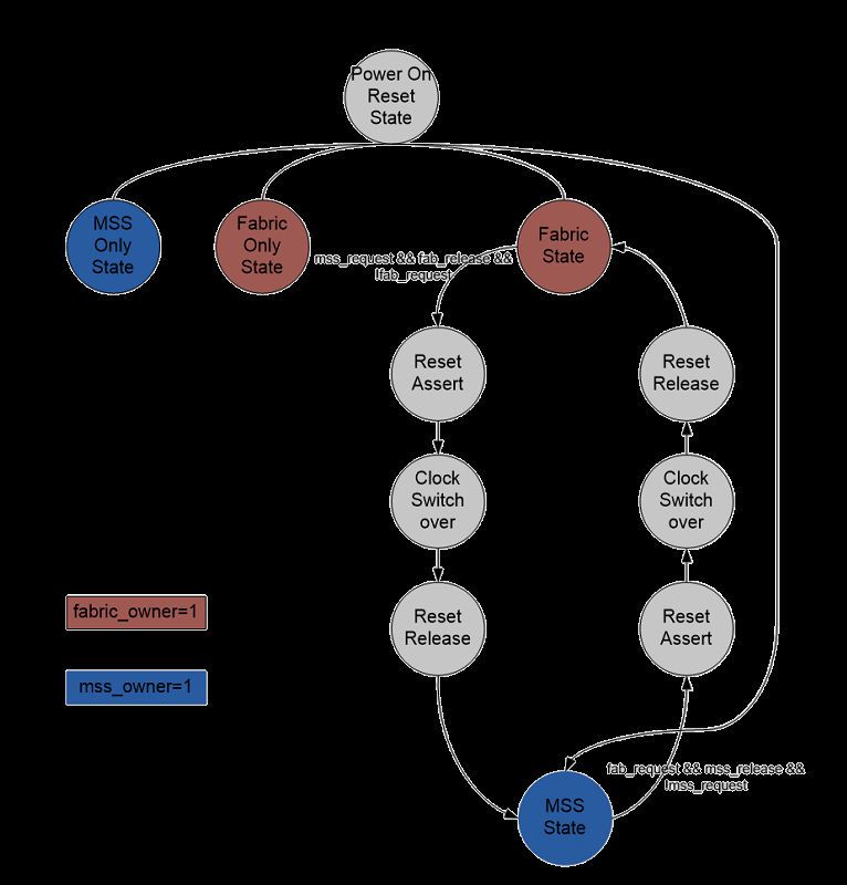
The Crypto block can be owned by either the fabric or MSS and the ownership can be transferred during operation.
Transfer of ownership requires co-operation between the MSS and Fabric designs.
© 2021 Microchip Technology Inc. User Guide DS50003088C-page 14
and its subsidiariesLibero® SoC v2021.2
Simulation Flow
Ownership Finite State Machine
The ownership FSM runs on the SCB clock that is independent of the FPGA fabric and MSS clocking systems.
During switchover events, the FSM will request that the SCB clock runs at 80 MHz rather than at 1 MHz idle rate.
Figure 2-2. Ownership Finite State Machine
2.3.1 Fabric Mode
In Fabric mode, streaming interface is not enabled. You can perform read and write operation using the AHB
interface.
Note: For more information about using Crypto block and performing simulation, see the AC464 Application Note:
PolarFire FPGA: Implementing Data Security Using User Cryptoprocessor.
© 2021 Microchip Technology Inc. User Guide DS50003088C-page 15
and its subsidiariesLibero® SoC v2021.2
Simulation Flow
2.3.2 MSS Mode
In MSS mode, only streaming interface simulations are supported. AHB interface is towards MSS and will not
be exposed to Fabric. Libero SoC generates PFSOC_MSS_FIC4_user.bfm file which can used to perform AXI
transaction with crypto engine. Streaming interface is also called direct transfer interface. The direct transfer interface
comprises of unidirectional data input and output ports, and associated handshakes for data transfer operations.
Direct transfers are performed when explicitly commanded by the direct transfer instructions.
2.3.2.1 DXI: Direct Transfer Block In
The DXI instruction copies a block of data from the direct transfer input port, xwdata, to the destination register
starting at the location determined by the IA/ASEL/AOP field. During the execution of the DXI instruction, the value
of the BOP field will be output on the xwaddr output port. The length of the transfer is given by the ALEN register.
Transfers are controlled by the xenable/xinaccept handshake and the DXI instruction will run until the specified
number of words have been transferred.
Table 2-7. Crypto DXI OPCODE and Operations
31 30 29 28 27 26 25 24 23 22 21 20 19 18 17 16 15 14 13 12 11 10 9 8 7 6 5 4 3 2 1 0
DXI: 0E IA ASEL AOP resv. BOP
Operation Condition Codes Registers
[ASEL](IA/AOP)←xwdata xwaddr←BOP — BER, MMR, TSR, FPR
PC←PC+1
Direct Transfer Input Interface Operation and Timing
The direct transfer input transaction occurs as the transmitting party drives xwdata and asserts xenable. The Crypto
block indicates that it will accept the data on the next rising edge of hclk by asserting the xinaccept signal. If the
xinaccept signal is negated, then the xenable and xwdata inputs will be ignored by the Crypto block. If the direct
transfer input port is not used, the xenable signal should be tied high and the xwdata signal should be tied to a
known value.
Figure 2-3. Crypto DXI Signal Waveform
To perform DXI operation in simulation, you need to provide write data on xwdata port of crypto engine. The following
steps are needed to perform a DXI transaction.
Steps to be followed in PFSOC_MSS_FIC4_user.bfm file:
1. Declare “CSR_MAIN” with the address
Example:
memmap CSR_MAIN 0x00007f80;
memmap LIR_BASE_ADDR 0x00004000;
2. Give the purge, soft reset and out of soft reset by writing the following commands.
write w CSR_MAIN 0x0 0x00000020 // set purge
wait 300
write w CSR_MAIN 0x0 0x00000001 // soft reset
wait 300
write w CSR_MAIN 0x0 0x00000000 // out of reset
wait 300
write w CSR_MAIN 0x0 0x00000002 // clear complete
© 2021 Microchip Technology Inc. User Guide DS50003088C-page 16
and its subsidiariesLibero® SoC v2021.2
Simulation Flow
3. Once the above steps are completed, configure some of the registers to perform the DXI transactions. The
following steps are the sequence to perform DXI transactions.
# Update Instructions
# Update Instructions in LIR registers, LIR register Address Range is from 4000h-5FFCh
# set the number of instruction user need to perform, set the number of instruction in
command with SLN as opcode at bits [31:26] and number of instructions at bit [22:13]
write w 0x4000 0x0 0x3010e1ce # SLN 0x087,0x1ce
# write the opcode in bits[31:26] and address at [22:13], [9:0] is the address which
user is able to see same address on xwaddr port while performing DXI transaction.
# opcode of DXI is 0XE.
write w 0x4008 0x0 0x3846a13f # DXI BER:0x235, BER:0x13f
write w 0x400c 0x0 0x74040800 # HLRA
# write the csrmain register to Start computation command bit
write w 0x7F80 0x0 0x10
#write the csrmain register to Write-only clear CMPLT flag bit
write w 0x00007f80 0x0 00000002
#read the csr main register
read w 0x00007f80 0x0 #
wait 300
4. Once the above steps are completed, wait for some time and read the data from the address. Address can be
calculated as DXI BER X 4 (0x235 X 4 =08d4).
You can read the data from address 0x8d4 till the length which was given in SLN register using 32_bit /64 bit
transactions.
You can get the same data that was given on the xwdata port when you do a read transaction in the BFM.
#Read data at BER:0x235
set offset 0x08d0
loop CNT 1 68 1
read64 w offset 0x0
set offset offset + 8
endloop
Steps to be followed in the testbench:
1. Once the crypto engine setup is done for DXI transfer by bfm master, you will receive
CRYPTO_XINACCEPT_M2F signal as high and CRYPTO_XWADDR_M2F as “13f”(which you set in the DXI
execution command). Assert CRYPTO_XENABLE_F2M and provide the data on CRYPTO_XWDATA_F2M.
2. Dessert the CRYPTO_XENABLE_F2M when CRYPTO_XINACCEPT_M2F is zero.
The following code block shows the example commands used in a design.
################################
########DXI INTERFACE##########
################################
procedure main;
memmap CSR_MAIN 0x00007f80;
memmap LIR_BASE_ADDR 0x00004000;
memmap FPR_BASE_ADDR 0x00003000;
memmap BER_BASE_ADDR 0x00000000;
int offset
int CNT
write w CSR_MAIN 0x0 0x00000020 // set purge
wait 300
write w CSR_MAIN 0x0 0x00000001 // soft reset
wait 300
write w CSR_MAIN 0x0 0x00000000 // out of reset
wait 300
write w CSR_MAIN 0x0 0x00000002 // clear complete
###################################################
# Update Instructions in LIR registers
#LIR Adress Range --4000h-5FFCh LIR Linear instruction register
# set the number of instruction command at bit [22:13]
write w 0x4000 0x0 0x3010e13h # SLN 0x087,0x1ce
### write the opcode in bits[31:26] and address at [22:13] and [9:0] is the address
## we see on xaddr while perfoming DXI transaction.
© 2021 Microchip Technology Inc. User Guide DS50003088C-page 17
and its subsidiariesLibero® SoC v2021.2
Simulation Flow
### opcode of DXI is 0XE.
write w 0x4008 0x0 0x3846a000 # DXI BER:0x235, BER:0x13f
write w 0x400c 0x0 0x74040800 # HLRA
write w 0x7F80 0x0 0x10 # write the csrmain register to Start computation command bit
write w 0x00007f80 0x0 00000002
#write the csrmain register to Write-only clear CMPLT flag bit
read w 0x00007f80 0x0
#read the csr main register
wait 300
#Read data at BER:0x235
set offset 0x08d0
loop CNT 1 68 1
read64 w offset 0x0
set offset offset + 8
endloop
return
2.3.2.2 DXO: Direct Transfer Block Out
The DXO instruction copies a block of data to the direct transfer output port, xrdata, from the source register starting
at the location determined by the IB/BSEL/BOP field. During the execution of the DXO instruction, the value of the
AOP field will be output on the xraddr output port. The length of the transfer is given by the ALEN register. Transfers
are controlled by the xvalidout/xoutack handshake, and the DXO instruction runs until the specified number of
words have been transferred.
Table 2-8. Crypto DXO OPCODE and Operations
3 3 2 2 2 2 2 2 2 2 2 2 1 1 1 1 1 1 1 1 1 1 9 8 7 6 5 4 3 2 1 0
1 0 9 8 7 6 5 4 3 2 1 0 9 8 7 6 5 4 3 2 1 0
DXO: 0F Reserve AOP I BSE BOP
d B L
Operation Condition Codes Registers
xrdata←[BSEL](IB/BOP) xraddr←AOP — BER, MMR, TSR, FPR
PC←PC+1
Direct Transfer Output Interface Operation and Timing
The direct transfer output transaction occurs as the rising edge of hclk, data is presented on xrdata, and the
xvalidout signal is asserted. The receiving party indicates receipt of the data by asserting the xoutack signal, which
is sampled on the rising edge of hclk by the Crypto block. The xoutack signal may be asserted on the same clock
cycle that xvalidout is asserted or any subsequent clock cycle. The following waveform shows an example where
the xoutack is asserted one cycle after xvalidout is asserted. If xvalid-out is negated, then the xoutack signal is
ignored.
Figure 2-4. Crypto DXO Signal Waveform
Following are the steps that need to be followed to perform DXO transaction.
Steps to be followed in PFSOC_MSS_FIC4_user.bfm file:
© 2021 Microchip Technology Inc. User Guide DS50003088C-page 18
and its subsidiariesLibero® SoC v2021.2
Simulation Flow
1. Declare “CSR_MIAN” with the address
Example:
memmap CSR_MAIN 0x00007f80;
memmap LIR_BASE_ADDR 0x00004000;
2. Give the purge, soft reset and out of soft reset by writing the following commands.
write w CSR_MAIN 0x0 0x00000020 // set purge
wait 300
write w CSR_MAIN 0x0 0x00000001 // soft reset
wait 300
write w CSR_MAIN 0x0 0x00000000 // out of reset
wait 300
write w CSR_MAIN 0x0 0x00000002 // clear complete
3. Once the above steps are completed write the at address that you are writing along with DXO op code and the
number of instructions that you are giving in SLN command.
write w 0x0b18 0x0 0x290cadba
write w 0x0b1c 0x0 0x85b3d5b1
.
.
.
.
write w 0x0c18 0x0 0x8f7f3ff6
4. After writing the write data, configure some of the registers to perform the DXO transactions. Perform DXO
transactions in the following sequence.
#Provide the number of instruction user need to perform, set the number of instructions
in command with
#SLN as opcode at [31:26] and address at bit [22:13]
write w 0x5000 0x0 0x300820a7 # SLN 0x041,0x0a7
# write the opcode in bits[31:26] and address where user need to write data at [9:0].
[22:13] is the address which user can see on xraddr while performing DXO transaction.
# opcode of DXO is 0XF.
write w 0x5004 0x0 0x3c6342c6
# DXO BER:0x31a, BER:0x2c6
write w 0x5008 0x0 0x74040800
# HLRA is the compulsory command we need to write
#write the csrmain register to Start computation command bit
write w 0x7F80 0x0 0x10
# to read the status of the transaction
read w 0x80000000 0x0
5. You will get the read data on xrdata port which is accessible to fabric.
Steps to be followed in the testbench:
1. Once the crypto engine setup is done for DXO transfer by bfm master you will receive
the CRYPTO_XVALIDOUT_M2F signal as high. Assert CRYPTO_XOUTACK_F2M and read data on
CRYPTO_XRDATA_F2M.
2. Dessert the CRYPTO_XOUTACK_F2M when CRYPTO_XVALIDOUT_M2F is zero.
3. You can get the same data that you wrote from the PFSOC_MSS_FIC4_user.bfm file.
The following code block shows the example commands for DXO interface used in a design.
################################
#########DXO INTERFACE##########
################################
procedure main;
memmap CSR_MAIN 0x00007f80;
memmap LIR_BASE_ADDR 0x00004000;
memmap FPR_BASE_ADDR 0x00003000;
memmap BER_BASE_ADDR 0x00000000;
int offset
int CNT
write w CSR_MAIN 0x0 0x00000020 // set purge
wait 300
write w CSR_MAIN 0x0 0x00000001 // soft reset
© 2021 Microchip Technology Inc. User Guide DS50003088C-page 19
and its subsidiariesLibero® SoC v2021.2
Simulation Flow
wait 300
write w CSR_MAIN 0x0 0x00000000 // out of reset
wait 300
write w CSR_MAIN 0x0 0x00000002 // clear complete
//writing the data in the adaress
//(adxo_adress divide by 4)
//which we are giving in the DXO regsiter
write w 0x0b18 0x0 0x290cadba
write w 0x0b1c 0x0 0x85b3d5b1
write w 0x0b20 0x0 0x5cead81e
write w 0x0b24 0x0 0x37295bce
write w 0x0b28 0x0 0xd4368de7
write w 0x0b2c 0x0 0x6e6a9a56
write w 0x0b30 0x0 0xcdc436d5
write w 0x0b34 0x0 0x88d7b83f
write w 0x0b38 0x0 0x19966aec
write w 0x0b3c 0x0 0x997bab2b
write w 0x0b40 0x0 0x8a468a5f
write w 0x0b44 0x0 0xa413c77b
write w 0x0b48 0x0 0x5968d480
write w 0x0b4c 0x0 0xa56447e3
write w 0x0b50 0x0 0xf2158e5b
write w 0x0b54 0x0 0xdc96b803
write w 0x0b58 0x0 0x6d2469c0
write w 0x0b5c 0x0 0x5a23c3ee
write w 0x0b60 0x0 0x5d704806
write w 0x0b64 0x0 0x01840f82
write w 0x0b68 0x0 0xb3843909
write w 0x0b6c 0x0 0x768f73b0
write w 0x0b70 0x0 0x74a771e6
write w 0x0b74 0x0 0x043cf308
write w 0x0b78 0x0 0x51e1eb8a
write w 0x0b7c 0x0 0xd5e33ef3
write w 0x0b80 0x0 0x7b4ac9e8
write w 0x0b84 0x0 0x501f4830
write w 0x0b88 0x0 0xa85a6c97
write w 0x0b8c 0x0 0xe893f45f
write w 0x0b90 0x0 0x81966fdd
write w 0x0b94 0x0 0x59d3d388
write w 0x0b98 0x0 0x01e420f6
write w 0x0b9c 0x0 0xa2ee76c3
write w 0x0ba0 0x0 0x86caf5bf
write w 0x0ba4 0x0 0xaab33ea9
write w 0x0ba8 0x0 0x1014d0f0
write w 0x0bac 0x0 0x6666031c
write w 0x0bb0 0x0 0xdec269f9
write w 0x0bb4 0x0 0x9d972097
write w 0x0bb8 0x0 0x7f251d52
write w 0x0bbc 0x0 0xe6d72245
write w 0x0bc0 0x0 0x0f5c6fac
write w 0x0bc4 0x0 0xebeea91d
write w 0x0bc8 0x0 0xda1da3d1
write w 0x0bcc 0x0 0xb6a81b9b
write w 0x0bd0 0x0 0xdbb136a3
write w 0x0bd4 0x0 0x6678b258
write w 0x0bd8 0x0 0xd1527aad
write w 0x0bdc 0x0 0xafd324e7
write w 0x0be0 0x0 0x207513b0
write w 0x0be4 0x0 0xf5ba6243
write w 0x0be8 0x0 0x1937ac22
write w 0x0bec 0x0 0x46a7fe06
write w 0x0bf0 0x0 0x2b00efc2
write w 0x0bf4 0x0 0x9b02fdc3
write w 0x0bf8 0x0 0x8555b4a5
write w 0x0bfc 0x0 0x8f564f8f
write w 0x0c00 0x0 0x0dc07d70
write w 0x0c04 0x0 0xd5953ef5
write w 0x0c08 0x0 0xb71ebd1f
write w 0x0c0c 0x0 0xf8ee65e3
write w 0x0c10 0x0 0x384a2df0
write w 0x0c14 0x0 0xaf708549
write w 0x0c18 0x0 0x8f7f3ff6
#Provide the number of instructions we need to perform
© 2021 Microchip Technology Inc. User Guide DS50003088C-page 20
and its subsidiariesLibero® SoC v2021.2
Simulation Flow
#set the number of instructions in command with
#SLN as opcode at [31:26] and address at bit [22:13]
write w 0x5000 0x0 0x300820a7 # SLN 0x041,0x0a7
### write the opcode in bits[31:26] and address at [9:0] and [22:13] is the address
## we see on xaddr while performing DXO transaction.
### opcode of DXO is 0XF.
write w 0x5004 0x0 0x3c6342c6 # DXO BER:0x31a, BER:0x2c6
write w 0x5008 0x0 0x74040800 # HLRA is the compulsory command we need to write
#write the csrmain register to Start computation command bit
write w 0x7F80 0x0 0x10
# To start read execution
read w 0x80000004 0x0
2.3.3 Shared MSS Mode
By default, Crypto is in MSS mode. In this mode, streaming interface simulations are supported. You can perform the
same operations which are performed in MSS mode.
To change Crypto from MSS mode to Fabric mode the following sequence needs to be followed.
Steps to be followed in PFSOC_MSS_FIC4_user.bfm file
Request crypto controller from MSS mode to Fabric mode by writing mss_release =1 and mss request =’b0;.
You can also perform this operation by writing IOWRITE is set to 2 in PFSOC_MSS_FIC4_user.bfm.
IOWRITE 0x00000002
Steps to be followed in the testbench
Once you have requested the Crypto controller from user.bfm file, assert CRYPTO_REQUEST_F2M and deassert
CRYPTO_RELEASE_F2M to change the mode from MSS mode to Fabric mode.
After changing into Fabric mode, you can perform the same operations which are performed in Fabric mode and
MSS interface will be disconnected from Crypto block.
2.3.4 Shared Fabric Mode
By default, Crypto is in Fabric mode. You can perform the same operations which are performed in Fabric mode. The
following steps are to change Crypto from Fabric mode to MSS mode.
Steps to be followed in PFSOC_MSS_FIC4_user.bfm file
Request the Crypto controller to change from Fabric mode to MSS mode by writing mss_release =0
and mss request =1’b1;. You can also perform this operation by writing IOWRITE is set to 1 in
PFSOC_MSS_FIC4_user.bfm.
IOWRITE 0x00000001
Steps to be followed in the testbench
Once you have requested crypto controller from user.bfm file, deassert CRYPTO_REQUEST_F2M and assert
CRYPTO_RELEASE_F2M to change the mode from Fabric mode to MSS mode.
2.4 DDR Controller
To enable fast simulation, the DDR controller follows a BFM behavioral model: It is a single model for “DDR controller
+ PHY + DDR Memory”, with no activity seen on the DDR pins connected to external DDR memory. DDR memory
is modeled as a sparse array, and performs address decoding and prints row, column, bank, and rank address
information in a simulation log.
© 2021 Microchip Technology Inc. User Guide DS50003088C-page 21
and its subsidiariesLibero® SoC v2021.2
Simulation Flow
Figure 2-5. Unused DDR
When no DDR memory is selected in MSS standalone configurator, in such case, if FIC is trying to access the DDR
memory then MSS simulation model displays the following message in the simulation log.
# DDR is set to unused in the MSS Configuration, cannot process AXI transaction with address
00c7000000.
The MSS standalone configurator configures the MSS DDR and generates configuration parameters. The simulation
model considers only the parameters in the following table.
Table 2-9. MSS DDR Configuration Parameter Support
MSS Configurator Considered Parameters
DDR_DDRC_CFG_CHIPADDR_MAP_CFG_CHIPADDR_MAP All possible values
DDR_DDRC_CFG_BANKADDR_MAP_0_CFG_BANKADDR_MAP_0 All possible values
DDR_DDRC_CFG_ROWADDR_MAP_0_CFG_ROWADDR_MAP_0 All possible values
DDR_DDRC_CFG_ROWADDR_MAP_1_CFG_ROWADDR_MAP_1 All possible values
DDR_DDRC_CFG_ROWADDR_MAP_2_CFG_ROWADDR_MAP_2 All possible values
DDR_DDRC_CFG_ROWADDR_MAP_3_CFG_ROWADDR_MAP_3 All possible values
DDR_DDRC_CFG_COLADDR_MAP_0_CFG_COLADDR_MAP_0 All possible values
DDR_DDRC_CFG_COLADDR_MAP_1_CFG_COLADDR_MAP_1 All possible values
DDR_DDRC_CFG_COLADDR_MAP_2_CFG_COLADDR_MAP_2 All possible values
DDR_DDRC_CFG_MEM_COLBITS_CFG_MEM_COLBITS All possible values
DDR_DDRC_CFG_MEM_ROWBITS_CFG_MEM_ROWBITS All possible values
DDR_DDRC_CFG_MEM_BANKBITS_CFG_MEM_BANKBITS All possible values
DDR_DDRC_CFG_NUM_RANKS_CFG_NUM_RANKS All possible values
DDR_DDRC_CFG_MANUAL_ADDRESS_MAP_CFG_MANUAL_ADDRESS_MAP All possible values
DDR_DDRC_CFG_MEMORY_TYPE_CFG_MEMORY_TYPE All possible values
DDR_DDRC_CFG_BG_INTERLEAVE_CFG_BG_INTERLEAVE All possible values
DDR_DDRC_CFG_BL_MODE_CFG_BL_MODE 8
DDR_DDRC_CFG_DQ_WIDTH_CFG_DQ_WIDTH All possible values
DDR_DDRC_CFG_CWL_CFG_CWL(DDR3/3L/4) All possible values
© 2021 Microchip Technology Inc. User Guide DS50003088C-page 22
and its subsidiariesLibero® SoC v2021.2
Simulation Flow
...........continued
MSS Configurator Considered Parameters
DDR_DDRC_CFG_CL_CFG_CL(DDR3/3L/4) All possible values
DDR_DDRC_CFG_WL_CFG_WL(LPDDR3/4) All possible values
DDR_DDRC_CFG_RL_CFG_RL(LPDDR3/4) All possible values
DDR_DDRC_CFG_CLK_FREQ All possible values
The simulation model has the following limitations.
Table 2-10. MSS DDR Model Limitations
Sr. No. Limitations
1 AXI transactions with 64-bit data only are supported. There is no support for word (32-bit)-,
halfword (16-bit)-, and byte (8-bit)-based AXI transactions.
2 Supports Burst Length of Fixed BL8 only.
In the context of page hits and page misses in real time applications, this simulation model always considers page
hits to avoid latencies caused by page misses.
You can access MSS-DDR from any FIC interface and can choose to share (compromise) bandwidth to the QoS
master. By default this QoS master is enabled and accesses the DDR with default configurations. Refer section QoS
Parameter for more details.
The fabric master can access the DDR memory with the following AXI address region.
Table 2-11. AXI Address Region
Type 64-bit Address Start 64-bit Address End 32-bit Address Start 32-bit Address End
Non-Cache access 0x14_0000_0000 0x17_ffff_ffff 0xc000_0000 0xcfff_ffff
Non-Cache WCB 0x18_0000_0000 0x1b_ffff_ffff 0xd000_0000 0xdfff_ffff
access
In DDR Memory Partition tab of MSS standalone configurator, the DDR memory is partitioned into Cached and
Non-Cached region as shown in the following figure.
© 2021 Microchip Technology Inc. User Guide DS50003088C-page 23
and its subsidiariesLibero® SoC v2021.2
Simulation Flow
Figure 2-6. DDR Memory Partition
The standalone MSS configurator calculates the Physical DDR offset for each region and this information is also
used by the MSS simulation model. Currently MSS-DDR simulation model supports access of Non-cache region only
from FPGA fabric.
Once user configures the MSS-DDR and creates a Libero project, they can launch the pre-synthesis simulation. The
following is an example of a simulation log of a fabric master, for example PCIe-BFM accessing MSS-DDR.
###########################################################################
# AMBA BFM Model
# Version 2.1 22Dec08
#
# Opening BFM Script file PCIE_1.vec
# Read 41 Vectors - Compiler Version 26.28
# BFM :Filenames referenced in Vectors
# PF_PCIE_C1_PF_PCIE_C1_0_PF_PCIE_PCIE_1_user.bfm
# BFM:22:writemultiple64 x c7000000 00000000 ... at 105 ns
# BFM: Data Write c7000000 0000000000000001
# BFM:24:readmultchk64 x c7000000 00000000 ... at 145 ns
# BFM: Data Write c7000008 0000000000000002
# Writing to DDR3 Memory @ rank = 0, bank = 00, row = 00700, col = 00000000, data = 00000001
# Writing to DDR3 Memory @ rank = 0, bank = 00, row = 00700, col = 00000001, data = 00000000
# Writing to DDR3 Memory @ rank = 0, bank = 00, row = 00700, col = 00000002, data = 00000002
# Writing to DDR3 Memory @ rank = 0, bank = 00, row = 00700, col = 00000003, data = 00000000
# Writing to DDR3 Memory @ rank = 0, bank = 00, row = 00700, col = 00000004, data = 00000003
# Writing to DDR3 Memory @ rank = 0, bank = 00, row = 00700, col = 00000005, data = 00000000
# Writing to DDR3 Memory @ rank = 0, bank = 00, row = 00700, col = 00000006, data = xxxxxxxx
# Writing to DDR3 Memory @ rank = 0, bank = 00, row = 00700, col = 00000007, data = xxxxxxxx
# BFM: Data Write c7000010 0000000000000003
# Reading from DDR3 Memory @ rank = 0, bank = 00, row = 00700, col = 00000000, data = 00000001
# Reading from DDR3 Memory @ rank = 0, bank = 00, row = 00700, col = 00000001, data = 00000000
# Reading from DDR3 Memory @ rank = 0, bank = 00, row = 00700, col = 00000002, data = 00000002
# Reading from DDR3 Memory @ rank = 0, bank = 00, row = 00700, col = 00000003, data = 00000000
# Reading from DDR3 Memory @ rank = 0, bank = 00, row = 00700, col = 00000004, data = 00000003
# Reading from DDR3 Memory @ rank = 0, bank = 00, row = 00700, col = 00000005, data = 00000000
# Reading from DDR3 Memory @ rank = 0, bank = 00, row = 00700, col = 00000006, data = xxxxxxxx
# Reading from DDR3 Memory @ rank = 0, bank = 00, row = 00700, col = 00000007, data = xxxxxxxx
# BFM: Data Read c7000000 0000000000000001 MASK:ffffffffffffffff at 385.000000ns
# BFM:27:return
# BFM: Data Read c7000008 0000000000000002 MASK:ffffffffffffffff at 395.000000ns
# BFM: Data Read c7000010 0000000000000003 MASK:ffffffffffffffff at 405.000000ns
#############################################################################
#
# PCIE1 BFM Simulation Complete - 3 Instructions - NO ERRORS
#
#############################################################################
© 2021 Microchip Technology Inc. User Guide DS50003088C-page 24
and its subsidiariesLibero® SoC v2021.2
Simulation Flow
You can disable the row, column related prints coming from the emulated DDR memory by using vsim commands as
described in following table.
Table 2-12. MSS DDR vsim Parameters
Parameter Description Value
DEBUG_MEM Enable/disable the prints coming 1: Prints row, column related
from DDR memory in simulation log information in simulation log (Default)
You can change the value of this 0: Does not prints row, column
parameter through vsim commands related information in simulation log
like below…
To disable the prints:
vsim -L polarfire -
L presynth -t 1ps -
gDEBUG_MEM=0 presynth.tb
The following is an example of a simulation log where PCIe-BFM accessing MSS-DDR with DDR memory and prints
are disabled.
###########################################################################
# AMBA BFM Model
# Version 2.1 22Dec08
#
# Opening BFM Script file PCIE_1.vec
# Read 41 Vectors - Compiler Version 26.28
# BFM :Filenames referenced in Vectors
# PF_PCIE_C1_PF_PCIE_C1_0_PF_PCIE_PCIE_1_user.bfm
# BFM:22:writemultiple64 x c7000000 00000000 ... at 105 ns
# BFM: Data Write c7000000 0000000000000001
# BFM:24:readmultchk64 x c7000000 00000000 ... at 145 ns
# BFM: Data Write c7000008 0000000000000002
# BFM: Data Write c7000010 0000000000000003
# BFM: Data Read c7000000 0000000000000001 MASK:ffffffffffffffff at 385.000000ns
# BFM:27:return
# BFM: Data Read c7000008 0000000000000002 MASK:ffffffffffffffff at 395.000000ns
# BFM: Data Read c7000010 0000000000000003 MASK:ffffffffffffffff at 405.000000ns
#############################################################################
#
# PCIE1 BFM Simulation Complete - 3 Instructions - NO ERRORS
#
#############################################################################
2.5 QoS Parameter
The QoS feature allows bandwidth to be shared for the fabric masters while accessing DDR. To share bandwidth,
an AXI master (referred as QoS master) is connected internally at the AXI switch that performs the DDR access.
This AXI master, which is hidden from you, performs DDR access controlled through QoS parameters. The QoS is
enabled only when DDR is enabled.
You can change the QoS parameter values using vsim commands while launching the simulation, to do so, see the
following table.
© 2021 Microchip Technology Inc. User Guide DS50003088C-page 25
and its subsidiariesLibero® SoC v2021.2
Simulation Flow
Table 2-13. MSS QoS Parameters
Parameter Description Default Value
QOS_AXI_CLKS Number of AXI clocks at which QoS master 5000
performs read/write AXI transactions with DDR.
To change the value of this parameter, use
vsim command as shown below:
vsim -L polarfire -L presynth -t
1ps –g
QOS_AXI_CLKS = 10000 presynth.tb
QOS_START_ADDRESS Base address for QoS operation. Change 38'h00_C000_0000
this address if the same address region is
being used by another application through FIC.
To avoid contention between QoS and FIC
accessing the same DDR region, shift the QoS
access region to an unused address region. To
change the value of this parameter, use vsim
command as shown below:
For 38-bit: vsim -L polarfire
-L presynth -t 1ps -
gQOS_START_ADDRESS=38'h1600000000
presynth.tb
For 32-bit: (also need to change
DDR_ADDRESS_REGION for 32-bit) vsim -
L polarfire -L presynth -t 1ps
-gQOS_START_ADDRESS=32'hcd000000 -
gDDR_ADDRESS_REGION=0 presynth.tb
NO_OF_QOS_TRANSACTIONS Number of burst read/write transactions 128 when DDR is
performed by QoS at regular or cyclic interval used.
of QOS_AXI_CLKS. If set to zero, QoS does not
perform any AXI transactions to DDR and the
entire bandwidth is allocated to FICs.
Note: Make sure the QOS_AXI_CLKS value is
much greater than the finish time of all QoS AXI
transactions. The smallest burst size typically
uses:
• 10 AXI clocks for read or write burst
transaction with DQ=16.
• 20 AXI clocks for read or write burst
transaction with DQ=16.
To change the value of this parameter, use
vsim command as shown below:
vsim -L polarfire -L presynth -
t 1ps -gNO_OF_QOS_TRANSACTIONS=512
presynth.tb
The following shows an example of a simulation log where a fabric QoS master accesses DDR with number of QoS
transactions set to ONE.
#
# QoS Write Transactions 1 Completed
# QoS Read Transactions 1 Completed
# Writing to DDR3 Memory @ rank = 0, bank = 00, row = 00000, col = 00000000, data = 12345678
# Writing to DDR3 Memory @ rank = 0, bank = 00, row = 00000, col = 00000001, data = aabbccdd
© 2021 Microchip Technology Inc. User Guide DS50003088C-page 26
and its subsidiariesYou can also read