NXP Connects i.MX 8 Family Hardware - Lydia Ziegler - Nxp corporate template, INTERNAL ...
←
→
Page content transcription
If your browser does not render page correctly, please read the page content below
NXP Connects i.MX 8 Family
Hardware
Lydia Ziegler
i.MX 8 DRAM Introduction and Tools Overview

October 2018 | AMF-AUT-T3361

                                              Company External – NXP, the NXP logo, and NXP secure connections for a smarter world are trademarks of
                                              NXP B.V. All other product or service names are the property of their respective owners. © 2018 NXP B.V.
Agenda
•   i.MX 8 Family Overview
•   i.MX 8QM/QXP DDR Controller
    Overview
•   i.MX 8QM/QXP DDR Initialization Flow
•   i.MX 8QM/QXP DDR Calibration Details
•   i.MX 8QM/QXP DDR Tools Introduction
•   Debugging DDR Failures

                             PUBLIC   1
i.MX Explosive Growth

                                                                                                  Over 460M i.MX
                                                                                                  SOCs shipped to
                                                                                                  date.

                                                                                                  Over 140M i.MX
                                                                                                  shipped in vehicles
                                                                                                  since 2007.

                                                                                                  #1 in eReaders

                                                                                                  #1 in Auto
                                                                                                  Infotainment
                                                                                                  Applications
                                                                                                  Processors

 2007   2008   2009   2010   2011          2012          2013   2014   2015   2016   2017

                                    i.MX          i.MX Auto

        Scalability • Trusted Supply • World Class Support
                                                                                     PUBLIC   2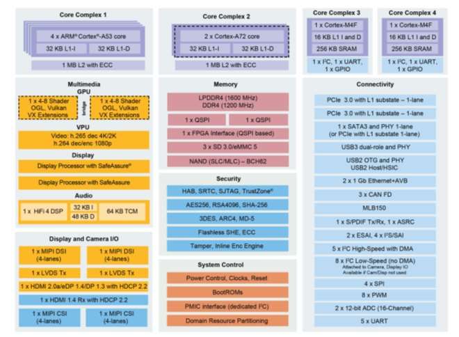
i.MX Automotive Roadmap

                          PUBLIC   3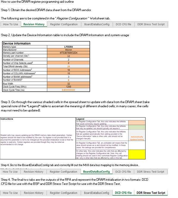
Scalability of Embedded Processing: i.MX Subsystem
Reuse
i.MX 8QM
A53 A53 A72 SCU
DSP
HSM
i.MX 8DualMax
A72 A72
M4 M4
A53 A53 SCU
M4 M4 DSP
HSM
i.MX 8QXP
1x GPU (8 s ha ders) 1x GPU (8 s ha ders)
A72 A35 A35
SCU
4K Video Di s play Controller Di s play Controller 1x GPU (8 shaders) M4 DSP
4K Video A35
HSM
i.MX 8DX
2x MIPI-DSI 2x LVDS PCIe PCIe 1GbE
Di s play Controller A35
SCU
1x GPU (4 s ha ders) A35 A35 M4 DSP
HSM
2x MIPI-CSI HDMI 2.0 Audio 1GbE MIPI-DSI 2x LVDS PCIe PCIe 1GbE
4K Video Di s play Controller
1x GPU (4 s ha ders)
i.MX 8DXL
x64 LPDDR4/DDR4 2x MIPI-CSI HDMI 2.0 Audio 1GbE
LVDS/MIPI LVDS/MIPI 1GbE 1080p Video i.MX 8SXL
USB 3.0 & 2.0 Di s play Controller A35 A35 M4
x64 LPDDR4/DDR4 A35
MIPI-CSI Audio 1GbE PCIe M4
USB 3.0 & 2.0 LVDS/MIPI LVDS/MIPI 1GbE
Pa ra llel
1GbE
Di s play SCU
x32 LPDDR4/DDR3L MIPI-CSI Audio PCIe 10/100 Pa ra llel
1GbE
USB 3.0 & 2.0 HSM Di s play SCU
PCIe 10/100
USB 2.0 HSM
x16 LPDDR4/DDR3L PCIe 10/100
USB 2.0 x16 LPDDR4/DDR3L USB 2.0
x16 LPDDR4/DDR3L
Most Scalable Family of Automotive Applications Processors for eCockpit,
Instrument Cluster, Display Audio and Telematics/V2X
PUBLIC 4
Automotive Applications Processor Roadmap
                                       ARM v5-v7                                                      ARM/v8                                                 ARM v8.2
  25-50k DMIPS
 128-300 GFLOPS
    eCockpit                                                                                                                                                  Next Gen
   big.LITTLE                                                                                                                                                 i.MX High
      Vision
                                                                           i.MX 8QuadMax
   Audio DSP

  15-20k DMIPS                                                             i.MX 8QuadPlus                 Pin Compatible Family
   64 GFLOPS
    eCockpit
                                                                                                                           i.MX 8DualMax
      Vision
   Audio DSP

                       i.MX 6Quad i.MX 6QuadPlus                            i.MX 8QuadXPlus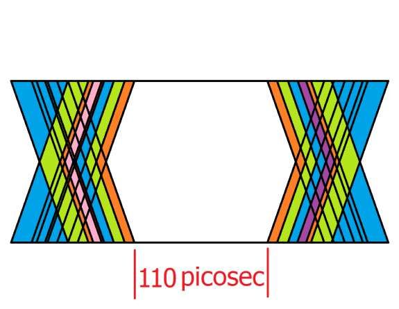
Automotive Applications Processor Roadmap
                                       ARM v5-v7                                                      ARM/v8                                                    ARM v8.2
  25-50k DMIPS
 128-300 GFLOPS
    eCockpit                                                                                                                                                     Next Gen
   big.LITTLE                                                                                                                                                    i.MX High
      Vision
                                                                           i.MX 8QuadMax
                                                                                                                                                  Pin Compatible
   Audio DSP                                                                                                                                    eCockpit Processors
                                                                                                          Pin Compatible Family                 • Up to 4x 1080p/ 1x 4k
  15-20k DMIPS                                                             i.MX 8QuadPlus                                                         Displays
   64 GFLOPS
                                                                                                                                                • x64 LP-DDR4 / 3200
    eCockpit
                                                                                                                           i.MX 8DualMax
      Vision                                                                                                                                    • HiFi4 DSP option
                                                                                                                                                       Next Gen
   Audio DSP                                                                                                                                    • Common
                                                                                                                                                       NextSoftware
                                                                                                                                                            Gen     and
                                                                                                                                                       i.MX
                                                                                                                                                       i.MX Entry
                                                                                                                                                            Entry
                                                                                                                                                  Hardware platform
                       i.MX 6Quad i.MX 6QuadPlus                            i.MX 8QuadXPlus
Automotive Applications Processor Roadmap
                                       ARM v5-v7                                                      ARM/v8                                                 ARM v8.2
  25-50k DMIPS
 128-300 GFLOPS
    eCockpit                                                                                                                                                  Next Gen
   big.LITTLE                                                                                                                                                 i.MX High
      Vision
                                                                           i.MX 8QuadMax
   Audio DSP

  15-20k DMIPS                                                             i.MX 8QuadPlus                 Pin Compatible Family
   64 GFLOPS
    eCockpit
                                                                                                                           i.MX 8DualMax
      Vision
   Audio DSP
                                                                                                                                Pin Compatible Display
                       i.MX 6Quad i.MX 6QuadPlus                            i.MX 8QuadXPlus                                      Audio and Instrument
Automotive Applications Processor Roadmap
                                       ARM v5-v7                                                      ARM/v8                                                     ARM v8.2
  25-50k DMIPS
 128-300 GFLOPS
    eCockpit                                                                                                                                                       Next Gen
   big.LITTLE                                                                                                                                                      i.MX High
      Vision
                                                                           i.MX 8QuadMax
   Audio DSP

  15-20k DMIPS                                                             i.MX 8QuadPlus                 Pin Compatible Family
   64 GFLOPS
    eCockpit
                                                                                                                           i.MX 8DualMax
      Vision
   Audio DSP

                       i.MX 6Quad i.MX 6QuadPlus                            i.MX 8QuadXPlus
Automotive Applications Processor Roadmap
                                       ARM v5-v7                                                      ARM/v8                                                 ARM v8.2
  25-50k DMIPS
 128-300 GFLOPS
    eCockpit                                                                                                                                                  Next Gen
   big.LITTLE                                                                                                                                                 i.MX High
      Vision
                                                                           i.MX 8QuadMax
   Audio DSP

  15-20k DMIPS                                                             i.MX 8QuadPlus                 Pin Compatible Family
   64 GFLOPS
    eCockpit
                                                                                                                           i.MX 8DualMax
      Vision
   Audio DSP

                       i.MX 6Quad i.MX 6QuadPlus                            i.MX 8QuadXPlus
Automotive Applications Processor Roadmap
ARM v5-v7 ARM/v8 ARM v8.2
25-50k DMIPS
128-300 GFLOPS
eCockpit Next Gen
big.LITTLE i.MX High
Vision
i.MX 8QuadMax
Audio DSP
15-20k DMIPS i.MX 8QuadPlus Pin Compatible Family
64 GFLOPS
eCockpit
i.MX 8DualMax Next Generation
Vision
Audio DSP i.MX 10
i.MX 6Quad i.MX 6QuadPlus
Scalable Family
i.MX 8QuadXPlusi.MX 8 & 8X Introduction
PUBLIC 11i.MX 8 Family of Automotive Applications Processors
GPU Display DSP Option Virtualization ARM CPU
• Dual Core GPU Cortex-M4 | Cortex-A53 | Cortex-A72
• 16 Vec4 Shaders Up to 4 displays Audio DSP SoC Level
8 • Up to 128 GFLOPS
OpenVX and ISI Vision Acceleration
• 64 execution units SoC OS
8 • High Speed total pixels
8QuadMax • Tessellation / Geometry
HiFi 4
Core
OS
OS
Software Compatibility
Shaders
Pin Compatibility
• Dual Core GPU
• 16 Vec4 Shaders Up to 4 displays Audio DSP SoC Level
8 • Up to 80 GFLOPS
• 64 execution units SoC OS
• Full Speed total pixels OS
8 Core
8QuadPlus • Tessellation/Geometry HiFi 4
OS
Shaders
• Single Core GPU
• 8 Vec4 Shaders Up to 3 displays Audio DSP SoC Level
• Up to 64 GFLOPS
8 • 32 execution units SoC OS
• High Speed total pixels Core
OS
8DualMax • Tessellation/Geometry
HiFi 4
OS
Shaders
Family of Scalable Automotive Multimedia Processors
eCockpit
Infotainment
Graphical Instrument Clusters PUBLIC 12preliminary
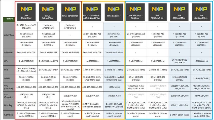
i.MX 8 Family – Block Diagrams i.MX 8QuadMax i.MX 8QuadPlus i.MX 8DualMax
Feature
29x29 Flip-Chip BGA 29x29 Flip-Chip BGA 29x29 Flip-Chip BGA
Package
0.75mm pitch 0.75mm pitch 0.75mm pitch
DMIPS (Cortex-A) 26k 18.5k 15k
ARM® Core
4x Cortex-A53 4x Cortex-A53 2x Cortex-A72
Complex 1
ARM® Core
2x Cortex®-A72 1x Cortex-A72 -
Complex 2
Display Controller 2x 2x 1x
GPU 2x GC7000 XSVX 2x GC7000Lite XSVX 1x GC7000 XSVX
MIPI CSI 2x 4-lane 2x 4-lane 2x 4-lane
MLB150 1x 1x via USB
HDMI In 1x 1x -
HDMI/eDP Out 1x 1x 1x
DDR 2x x32 2x x32 2x x32
PCIe 2x PCIe 3.0 2x PCIe 3.0 2x PCIe 3.0
SATA 1x SATA3 1x SATA3 -
1x 1Gb w/AVB
Ethernet 2x 1Gb w/AVB 2x 1Gb w/AVB
1x 10/100 w/AVB
PUBLIC 13Preliminary – Subject to Change
i.MX 8X Family of Applications Processors
GPU Video Displays DSP USB DDR ARM CPU
• Single Core GPU x32 Cortex-A35 + M4
• 4 Vec4 Shaders Up to 3
high performance
4 • 16 execution units 2x 1080p
1x WVGA
DDR3L-1866
(ECC option)
• OpenGL ES 3.1
8QuadXPlus • OpenCL Embedded + Legacy HiFi 4 LP-DDR4-2400
(no ECC)
Software Compatibility
Pin Compatibility
• Single Core GPU Up to 3 x32
• 4 Vec4 Shaders
2x 1080p DDR3L-1866
4 high performance
• 16 execution units 1x WVGA (ECC option)
• OpenGL ES 3.1 HiFi 4 LP-DDR4-2400
8DualXPlus • OpenCL Embedded + Legacy (no ECC)
• Single Core GPU x16
Up to 3
• 4 Vec4 Shaders DDR3L-1866
4 poweroptimized
• 16 execution units
2x 1080p
1x WVGA
(no ECC)
• OpenGL ES 3.1 + Legacy HiFi 4 LP-DDR4-2400
8DualX • OpenCL Embedded (no ECC)
Family of Scalable Automotive Multimedia Processors
Display Audio Applications
Graphical Instrument Clusters
Telematics and V2X
PUBLIC 14i.MX 8X Family Block Diagram
Core Complex 2
i.MX 8DualXPlus i.MX 8DualX
Core Complex 1 Connectivity
1x Cortex-M4F
i.MX 8QuadXPlus
1x I2C
4x 4x UART Feature
2-4xCortex-A53
Cortex-A35 16KB L1 I-cache
32KB
32KBL1-D
L1-D 1x UART
32KB L1-I 32KB
32KBL1-I 32KBL1-D
L1-D 16KB L1 D-cache 8x I2C
6x GPIO
2 x Cortex-A35
512KB L2 w/ECC
256KB SRAM 1x TPM Timer 4x SPI (i.MX 8DualXPlus)
ARM® Core 2 x Cortex-A35
2x Gbit Ethernet 4 x Cortex-A35
Multimedia Memory
(i.MX 8QuadXPlus)
DDR3 @933 MHz (ECC Option)
GPU 1x 10/100 Ethernet
LPDDR4 @ 1200 MHz (no ECC)
3.3V / 1.8V GPIO
ARM® Core 1 x Cortex-M4F 1 x Cortex-M4F
4- Shaders 2x SDIO3.0/eMMC5.1
OpenGL ES 3.1 DSP Core Tensilica® HiFi 4 DSP Tensilica HiFi 4 DSP
Vulkan® 2x Quad / 1x Octal SPI PCIe 3.0 with L1 Substate (1-lane)
VPU
RAW NAND – BCH62 1x USB3 OTG w/PHY *32-bit DDR3L (ECC option) 16-bit DDR3L (no ECC)
Video: h.265 dec 4k DRAM
h.264 dec/enc 1080p 1 or 2x USB2 OTG w/PHY LPDDR4 (no ECC) LPDDR4 (no ECC)
Security
Audio 3x CAN/CAN FD 1 x GC7000Lite 1 x GC7000Lite
HAB, SRTC, SJTAG, TrustZone
1x Tensilica® GPU
HiFi 4 DSP 32KB I 48KB D
High Performance Power Optimized
AES256, RSA4096, SHA-512 MOST 25/50
512 KB SRAM 64KB TCM 3DES, ARC4, MD-5 4K h.265 dec, 1080p h.264 1080p h.264 enc/dec
4x4 Keypad VPU
enc/dec
Flashless SHE, ECC
4x PWM
Display & Camera I/O Tamper detection, Inline Enc Engine
1 x Gigabit with AVB
1x 12-bit ADC Ethernet 2 x Gigabit with AVB
1 x 10/100
Display Processor w/ SafeAssure® System Control
2x ASRC, SPDIF
2 x MIPI-DSI/LVDS Combo PHY* Power Control, Clocks, Reset
4x SAI, ESAI, MQS USB with 1 x USB 3.0 (or USB 2.0)
1x Parallel Display Boot ROMs 2 x USB 2.0
PHY 1 x USB 2.0
1x MIPI CSI PMIC interface (dedicated I2C)
1x Parallel CSI Resource Domain Partitioning
Varies by device
*21x21 package only.
17x17 will have 16-bit memory interface
* Each single PHY can either be a 1×4 lane MIPI-DSI or a 1×1 channel LVDS interface for a total of 2 display interfaces.
In combination, the two PHYs can be configured to be a single 2-channel LVDS interface.
PUBLIC 15i.MX 8QM/QXP
DDR Controller Overview
PUBLIC 16DDR Controller/PHY Features
• i.MX 8QM
− Supports LPDDR4 up to 3200Mbps (1.6GHz DDR clock)
− Supports DDR4 up to 2400Mbps (1.2GHz DDR clock)
− Two DDR Controllers (4KB interleave between controllers)
• i.MX 8QXP
− Supports LPDDR4 up to 2400Mbps (1.2GHz DDR clock)
− Supports DDR3L (with ECC) up to 1866Mbps (933MHz DDR clock)
− One DDR Controller
• Data bus width 32-bits/16-bits for all DDR protocols.
• Supports up to 2 ranks for all DDR protocols
• Voltage and temperature compensation in the background
PUBLIC 17DDR Subsystem Architecture
DDR Controller
DRC
RRB
PHYv1 28FDSOI Up to 32-bit data bus along
uMCTL2 with associated DQS/DM
control signals
data training
Scheduler
and SDRAM
AXI Port Arbiter command PHY
generator
(DDRC) PHY PLL
Address and control signals
are configurable based on
PUB DRAM type
WB
• QM has two sets of DDR controllers/PHYs
• QX has one DDR controller/PHY
PUBLIC 18Comparison With i.MX6/7
• i.MX 6 series uses the MMDC
• i.MX 8QM/QXP and i.MX7D uses 3rd party IP
− DDR Controller IP similar programming model with i.MX7D
− DDR PHY is completely different from MX7D
• i.MX 8QM/QXP DDR is higher speed
− Ultra high speed, more challenges for customer PCB design
− Previous i.MX max DDR freq 528MHz, i.MX 8 QM up to 1.6GHz
− Follow layout recommendations provided in the Hardware Developers Guide
PUBLIC 19i.MX 8QM/QXP and i.MX 8M High-level Comparison
Feature i.MX8 QM/QXP i.MX8M
System Control Unit (SCU) Yes No, architecture similar to
MX7D
DDR Initialization Performed by SCU Perform by SPL
Automatic Data training Performed as part of Performed by the PHY
initialization script (PIR MCU (firmware loaded into
writes) MCU IRAM/DRAM)
Controller version SNPS DDR Controller SNPS DDR Controller
(dwc_ddr_umctl2) (dwc_ddr_umctl2)
PHY version SNPS PHY v1 SNPS PHY v2 (integrated
MCU)
PUBLIC 20High Level Feature Set Comparison of the i.MX 8 / 8X / 8M
Families
QM Family QX Family mScale Family
PUBLIC 21i.MX8 QM i.MX8 QXP
DDR Pin IO name
DCF_00
DCF_01
LPDDR4 name DDR4 name
CA2_A
CA4_A
A5
A6
IO name
DCF_00
DCF_01
LPDDR4 name
CA2_A
CA4_A
DDR3 name
A5
A6
Function DCF_02
DCF_03
DCF_04
CA5_A
ALERT_N
A7
A8
DCF_03
DCF_04
DCF_05
CA5_A A7
A8
A9
DCF_05 A9
DCF_07 RAS#
DCF_06 BG1
DCF_08 CA3_A A3
DCF_07 ACT_N
DCF_08 CA3_A A3 DCF_09 ODT_CA_A ODT
DCF_09 ODT_CA_A ODT DCF_10 CS0_A A1
• Pins configurable DCF_10 CS0_A A1 DCF_11 CA0_A A0
DCF_11 CA0_A A0 DCF_12 CS1_A A2
based on DDR type DCF_12 CS1_A A2 DCF_14 CKE0_A
DCF_13 PARITY DCF_15 CKE1_A
• Refer to NXP board DCF_14 CKE0_A DCF_16 CA1_A A4
DCF_15 CKE1_A
schematics for DCF_16 CA1_A A4
DCF_17
DCF_18
CA4_B
RESET_N
A12
RESET#
DCF_17 CA4_B A12
examples DCF_18 RESET_N RESET_N
DCF_19 CA5_B A14
DCF_19 CA5_B A14 DCF_20 A15
DCF_20 A15 DCF_21 BA0
DCF_21 BA0 DCF_22 BA1
DCF_22 BA1 DCF_23 BA2
DCF_23 BG0 DCF_24 CAS#
DCF_24 A17 DCF_25 ODT_CA_B
DCF_25 ODT_CA_B ODT1 DCF_26 CA3_B A13
DCF_26 CA3_B A13
DCF_27 CA0_B A10
DCF_27 CA0_B A10
DCF_28 CS0_B CS_N[0]
DCF_28 CS0_B CS_N[0]
DCF_29 CS1_B CS_N[1]
DCF_29 CS1_B CS_N[1]
DCF_30 CKE0_B CKE0 DCF_30 CKE0_B CKE0
DCF_31 CKE1_B CKE1 DCF_31 CKE1_B CKE1
DCF_32 CA1_B A11 DCF_32 CA1_B A11
DCF_33 CA2_B A16 DCF_33 CA2_B WE#
PUBLIC 22JEDEC Timing
PUBLIC 23Timing Budget for Read – JEDEC Min From LPDDR4
• 1.6 GHz frequency has a clock period of 625 picoseconds
− Double data rate gives a theoretical window of 312.5 picoseconds
• JEDEC standards require LPDDR4 to have a minimum window of 70% of
theoretical window (94 picoseconds)
− Accounts for all skew, slew rate diff and jitter from LPDDR4 package
PUBLIC 24Timing Budget for Read – Processor Flip-Flop times
• Set up time requirement for Read FIFO of processor
− 17 picoseconds
• Hold time requirement for Read FIFO of processor
− 17 picoseconds
PUBLIC 25Timing Budget for Read – Vref Uncertainty
• Vref must meet the following tolerance: +/- 1%
− Vref effects the time that a signal (DQ/DM/CA) is latched into the pads
• Timing fluctuations for maximum Vref variations
−4 picoseconds for Set Up
− 4 picoseconds for Hold
PUBLIC 26Timing Budget for Read – DQS Placement Uncertainty
• Accounts for Delay Element granularity in DLL
− One delay element is ~ 5 picoseconds long
− Manufacturing process variations can change this value.
• Timing budget for DQS variation is 7 picoseconds applied to Set Up
PUBLIC 27Timing Budget for Read – Voltage-Temperature Drift
• ZQ Calibrations account for signal drive strength on PCB
• Variations in Volt-Temp effect delay element time
• Timing budget for maximum allowed Volt-Temp drift
−7 picoseconds for Hold
PUBLIC 28Timing Budget for Read – Tap Size Variation
• The actual delay element tap point may vary
• Timing budget allows for 2.2 picoseconds based on manufacturing
process variations.
PUBLIC 29Timing Budget for Read – Power Supply Noise
• Maximum allowed internal power rail ripple is +/- 2%
• Accounts for jitter introduced on Read signal from package ball to the input
of the Read FIFO.
• Timing budget allowances:
− Set Up: 8 picoseconds
− Hold: 8 picoseconds PUBLIC 30Timing Budget for Read – I/O Rise/Fall Skew mismatch
• Accounts for internal Rise/Fall mismatches of the Read signal from the processor
balls to the Read FIFO.
• Typically caused by different slew rates for rising and falling edges
• Timing budget allowances:
− Set Up: 9 picoseconds
− Hold: 9 picoseconds
PUBLIC 31Timing Budget for Read – InterSymbol Interference ISI
• Accounts for interactions between data traces internal to the processor,
processor balls to the Read FIFO.
• Timing budget allowances:
− Set Up: 8 picoseconds
− Hold: 8 picoseconds
PUBLIC 32Timing Budget – Allowance for Trace Length Mismatch
• The remaining Timing Budget is allocated to PCB trace length, internal
package length, and design margin.
• For most robust design, recommend match trace lengths as close as
possible:
− Addthe internal package length given to the PCB trace length, and then match lengths by
group.
PUBLIC 33Timing Budget
• As DDR frequency increases, the time between strobe edges (rise/fall) becomes
so small that the DRAM system designer needs to account for all possible errors
in timing.
• The frequency itself provides the maximum available time in a window.
• The three major components in a DRAM system can account for all errors:
− The DRAM Device
− The PHY on the processor
− The interconnecting system ~ PCB board.
▪ Includes package substrate up to silicon pads.
▪ IBIS models include necessary information.
At 1.6 GHz, the maximum data window is 313 picoseconds. Uncertainties on the DRAM and processor
reduce this window to 110 picoseconds. If further errors on the PCB amount to more than 110
picoseconds, there are potential problems with data integrity.
PUBLIC 34i.MX 8QM/QX
DDR Initialization Flow
PUBLIC 35DDR Initialization Flow
• Three main initialization components DDR Controller/PHY
register initialization
− Controller/PHY initialization
− DRAM initialization
− Data training DRAM initialization
• Data training (calibration) part of init flow
− Data training specific to DRAM technology
DRAM training
• Initialization sequence must adhere to LP4 DDR4 DDR3
order shown here
− Includes sequence order for data training
• DDR Register Programming Aid (RPA) PHY/DRAM Ready
takes care of this
PUBLIC 36i.MX 6 Versus i.MX 8QM/QXP DDR Initialization Process
i.MX 6 Series i.MX 8QM/QX
1. Create an initial DRAM initialization script 1. Create an initial DRAM initialization script
from RPA from RPA
2. Run initial DRAM initialization 2. Run DDR stress test based on the script
3. Run calibration and then test to make sure 3. Tweak the script (if necessary) to make sure
board works it can pass on several boards
4. Run calibration on a number of boards and
obtain average values
5. Place averaged calibration values into
DRAM initialization script
6. Run updated DRAM initialization
7. Perform testing on several boards
PUBLIC 37i.MX 8QM /QX
DDR Calibration Details
PUBLIC 38DDR Data Training
LPDD DDR4 DDR3
• Different DDR technology R4
require different data
training
• Data training part of
initialization process
− Write PIR register
− Poll for completion
• Command Bus Training
(CBT) not automatic,
requires SW algorithm
− Currently
under investigation
and development by R&D
PUBLIC 39DDR Training/Calibration Introduction
DRAM Calibration LPDDR4 DDR4 DDR3L
Impedance (ZQ) calibration ✓ ✓ ✓
Command/address bus ✓
training*
Write Leveling ✓ ✓ ✓
DQS Gate training ✓ ✓ ✓
Write DQS2DQ training ✓
Data Eye training ✓ ✓ ✓
VREF training ✓ ✓
* Command Bus Training (CBT) not automatic, requires SW algorithm; currently under investigation and development by R&D
PUBLIC 40DDR Training (calibration) During Initialization
• Reason for data training (calibration) during DRAM initialization
− New DRAM technologies increasingly faster
− Tighter timings affected by delays between PHY and DDR memory
▪ Factors like board trace length affect these delays
▪ Process variations of the SoC and DRAM may also affect these delays
− JEDEC requires data training for LPDDR4 and DDR4 as part of the initialization
• Data training implemented completely by DDR PHY
− Some setup may be needed (i.e. enable/disable DQS pull up/down for DQS gate)
− Simple write to PHY PIR to start training then poll PHY PGSR0 for training complete
− RPA handles all of this, no user interaction
• No longer need to manually run calibration on various boards to take an average
(as in the case of previous i.MX SoC)
PUBLIC 41DDR Calibration After Initialization (Run-time)
• Run-time calibration during DRAM operation compensates for variations in voltage and temperature
• Enabled during initialization of the DRAM, no further user interaction required
− Delay line VT compensation
▪ Delays vary over time due to voltage and temperature fluctuations
▪ PHY contains circuits to monitor delay in the background during DRAM operation
▪ Drift compensation logic periodically adjusts delay line select input for variations in voltage/temperature
▪ Ensures each delay line maintains a constant time delay as voltage and temperature change during chip operation
− Impedance (ZQ) calibration
▪ PHY has background calibration/compensation engine
▪ Boot time: during PHY initialization, full calibration performed to find initial values
▪ Run time: during DRAM operation
• ZQ calibration periodically calibrates the output driver impedance and ODT of SoC and DRAM I/Os
• Incremental compensation performed in the background
− DQS drift detection (applicable only to LPDDR4)
▪ PHY logic monitors drift in read DQS signal compared to DQS_GATE input due to DRAM tDQSCK variations over time
▪ tDQSCK for DDR3/4 are kept relatively constant by DRAM and hence do not require DQS drift detection
PUBLIC 42DDR Calibration Modes
• Impedance (ZQ) calibration Occurs as part of PHY initialization and run-time
• Command/address bus training*
• Write Leveling
• DQS Gate training
• Write DQS2DQ training* Performed by PHY during initialization
• Data Eye training
• VREF training**
Note: The items of DQ training are performed automatically during DRAM initialization by the DDR PHY.
Specifically, each of these trainings are simply triggered by programming their specific bits in the
PHY Initialization Register (PIR).
* Applicable only to LPDDR4
** Applicable only to LPDDR4 and DDR4
PUBLIC 43Impedance (ZQ) Calibration
What
ZQ calibration calibrates I/O driver impedance across PVT
Why
This automatic process tunes the DRAM and the SoC I/O Pad output drivers (drive strength) and ODT values
across changes in process, voltage, and temperature.
How
ZQ calibration is performed as part of the DRAM initialization process.
Auto ZQ calibration is configured via the register DDRC_ZQCTL0 during DRAM initialization
When
ZQ calibration is configured during DRAM initialization to run periodically. Once configured, there is no further
user interaction required.
PUBLIC 44Command/Address Bus Training (LPDDR4 only)
What
Command/Address Bus Training (CBT) used to center Command/Address bus (CS and CA[5:0]) with rising
clock edge by adjusting internal delays associated with CA bus
CA
Why
Higher DRAM speeds implies more stringent timing. However, LPDDR4 CA bus is single data rate thereby
increases timing margin when compared to double data rate.
How
QM/QX SNPS PHYv1 does not perform CBT automatically (within JEDEC spec by default). Requires software
algorithm, under investigation by R&D.
When
JEDEC recommends but does not require CBT to be performed during initialization. Another proposal is to run
CBT on a few boards to obtain an average CA delay value and apply to initialization.
PUBLIC 45Write Leveling
What
Compensates for CK to DQS timing skew by aligning clock
with data strobe to improve signal integrity performance
Why
• For non-LPDDR4: compensates for skew between clock
and data strobe caused by fly-by topology
• LPDDR4: compensates for CK-to-DQS timing skew
affecting timing parameters such as tDQSS (write
command to 1st DQS latching), tDSS and tDSH (DQS
setup/hold time)
How
DDR PHY invokes write leveling mode in SDRAM then
delays DQS to align with clock at SDRAM
When
Write leveling training is performed automatically by the
DDR PHY during DRAM initialization
PUBLIC 46DQS Gate Training
What
Training that sweeps read DQS gate over possible gating positions to discover appropriate placement
Why
• PHY internally gates DQS during non-read operations to prevent erroneous latching of DQS edges
• Precise alignment of gate within read preamble a prerequisite for proper reads
• Delays (such as board trace lengths) in read path are imprecisely known, need to train the gate for a particular system
How
DQS Gate training is performed automatically by the DDR PHY. The PUB features a built-in read DQS strobe gate training unit that
may be triggered as part of the initialization process using the PIR register
When
DQS Gate training is performed automatically during DRAM initialization.
PUBLIC 47Write DQS2DQ Training (LPDDR4 only)
What
DQS to DQ training is referred to as “Write training” in JEDEC and “Write DQ training” in DFI.
Why
LPDDR4 Memory devices use an unmatched DQS-DQ path to enable high-speed performance and save
power. As a result, the DQS strobe must be trained to arrive at the DQ latch center-aligned with the data eye.
How
The DQ receiver will latch the data present on the DQ bus when DQS reaches the latch, and DQS2DQ training is
accomplished by delaying the DQ signals relative to DQS such that the data eye arrives at the receiver latch
centered on the DQS transition. Above picture shows the DQ position after the training.
When
DQS2DQ training is performed automatically by the DDR PHY during DRAM initialization.
PUBLIC 48Data Eye Training
What
The PHY training firmware contains automatic training sequences to perform read and write de-skew which aligns
the data bits to the DQ bit with the longest delay using a bit delay line (BDL). After performing bit de-skew the read
and write eye centering training is executed to place the strobe in the center of the eye defined by the bits in the
respective byte. Below is an illustration of before and after de-skewing and centering.
Before After
Why
As bit rates increase to 2133Mbps and beyond, maintaining timing margins in the DDR interfaces has
become more difficult. The PHY solution includes delay lines to compensate for per-bit skew due to factors
such as PHY to IO routing skews, package skews, PCB skew, etc.
When
Read/write de-skew and eye centering is performed automatically by the DDR PHY during DRAM initialization.
PUBLIC 49VREF Training (LPDDR4 and DDR4)
What
• Write/read eyes should be as wide as possible to provide stable/robust
memory access.
• Eye position depends upon LCDL (delay line) and VREF values.
Why
• VREF is internally generated by SoC and DRAM.
• VREF training used to determine range of VREF values where memory
interface (write/read) is stable and then find out an optimum write/read
eye position.
The following types of VREF training are supported:
DRAM VREF Training: Optimizes the write eye by sweeping DRAM VREF
DQ values inside memory.
Host (i.MX8) VREF Training: Optimizes the read eye by sweeping the PHY
I/O’s VREF setting.
How
VREF training is performed automatically by the DDR PHY during DRAM
initialization.
Note, for DDR3L, VREF is externally supplied hence there is no VREF training requirement.
PUBLIC 50i.MX 8QM/QXP DDR Tool
Introduction
PUBLIC 51i.MX 8QM/QX DDR Register Programming Aid (RPA)
Highlights
• Developed by SE team and no formal roll out or maintenance
− Based on scripts provided by design/validation
• Excel spread sheet based, transparent, ease-of-use
• Help to compute DDRC registers configuration
− JEDEC timing parameters
− DDRC DFI timing parameters
− DDRPHY configuration
• Help to configure DDR mode registers
• Includes necessary data training for specific memory type
• “BoardDataBusConfig” worksheet for data bus swizzling
• Two output formats
− DCD CFG file – SCFW usage (copy into SCFW board folder)
− DDR Stress Test Script – for use with the DDR stress test
PUBLIC 52i.MX 8QM/QX RPA
• Each tool based on DDR technology:
LPDDR4, DDR4 or DDR3
• Applies correct order of initialization
steps
− Controller/PHY initialization
− DRAM initialization
− Data training
• Includes worksheet for data bus
mapping
− Configures relevant registers for data bit/byte
swizzling
• Generates two initialization formats
− CFG file for use with SCFW (save as .cfg)
− DDR Stress Test Script (save as .ds)
• Color coded cells provides usage
guidance
PUBLIC 53RPA – Register Configuration
• In most cases, user only needs to update Device Information table
− Automatically updates configuration and timings (all timings are based on JEDEC
standard)
− No need to manually go through all register fields (strongly recommend to not manually
edit those fields)
Indicates the DDR type the RPA is applicable to
Recommend to list vendor and exact part number
User must ensure these are accurate; values are found in
the memory device data sheet
PUBLIC 54RPA – BoardDataBusConfig
• Board layout guidelines allow users to swizzle data bits within a byte
lane and swap byte lanes
• “BoardDataBusConfig” worksheet – users input SoC data bus
connection
− Data bus mapping must be accurate for PHY data training
− Relevant registers are automatically updated
User must accurately populate this field based on the
customer schematics. Errors in this field may result in data
training errors.
PUBLIC 55RPA – Initialization Scripts
• Two file formats, simply copy-and-paste into text document:
− [DCD CFG file] for SCFW (to support SCFW porting) – save as .cfg
− [DDR Stress Test Script] for use with DDR stress test – save as .ds
• Strongly recommend to not manually edit these tabs
− Make changes only to Register Configuration and BoardDataBusConfig tabs
DCD CFG file example DDR Stress Test Script example
• Yellow cells indicates that they are affected by changes on the Register Configuration and
BoardDataBusConfig tabs
PUBLIC 56i.MX 8QM/QX DDR Stress Test Tool – Overview
• Supports i.MX 8QM/QX DDR Stress Test Folder structure
• Board hardware requirement
− USB OTG port for Serial download mode
− Debug AP UART port*
− Highly recommend SCU UART port
DDR Stress Test
• Requires functional SCFW GUI
• Use RPA to generate stress test
script
* Note, for Win10, may require
manually installing COM port driver
(FTDI, SiLabs,…)
PUBLIC 57i.MX 8QM/QX DDR Stress Test Tool – High Level Steps
• User must first ensure working SCFW
• Create a new DDR script by RPA tool
− Based on DDR device and board hardware design
• Power on i.MX 8QM/QX board in serial download mode
− USB OTG and AP UART port connect correctly
− Highly recommend SCU UART port connection to serial terminal
• Load DDR script and download i.MX8 QM/QX binaries to target board
• If DDR Stress Test passes, use RPA DCD CFG file to create *.cfg file for
SCFW
− Rebuild SCFW with updated *.cfg and proceed with u-boot/OS porting
− Recommend running OS stress test (i.e. memtester)
PUBLIC 58i.MX 8QM/QX DDR Stress Test Tool – SCFW
• User must first port SCFW to customer board (ensure SCFW is up and
running)
• Then build the SCFW for the DDR Stress Test
make qx R=B0 DDR_CON=ddr_stress_test_parser
− SCFW will run a special “parser” instead of running DDR init
− DDR Stress Test loads ddr initialization to OCRAM then “parser” executes init
− Copy and re-name scfw_tcm.bin to DDR Stress Test bin folder as follows:
▪ QM: mx8qm_scfw_download.bin
▪ QX: mx8qx_scfw_download.bin
• SCU UART port connection to serial terminal
− Ensures SCFW is up-and-running
PUBLIC 59i.MX 8QM/QX DDR Stress Test Tool – How to Run
1. Select the correct COM port 3. When AP UART, DDR script, and
number for the AP UART, then hit SoC selected, hit Download
connect
2. Select the desired DDR initialization
script and SoC
4. Select operational features
5. Select freq range for test or
leave as 0 for testing at target freq
Double check DDR
parameters and ensure
they match what’s on the
6. Hit Stress test to start running
board
DDR data training
status
PUBLIC 60DDR Stress Test Fails to Run – Common Causes
• DDR Stress Test should run even when data training error occurs
• However, in some corner cases, the DDR Stress Test may fail to run
• Make sure board is in serial download mode and USB OTG is connected
Example of successful SCFW execution
• If all you see is this, first make sure the SCFW is properly running (check
SCFW UART port)
• Make sure to build the SCFW for the DDR Stress Test
• If SCFW hangs during DDR init, make sure you are selecting the correct
*.ds file (in other words, don’t select a QM *.ds file when using QX)
• If SCFW is successful and DDR init has completed, then check to make
sure you are connected to the correct COM port for the AP UART
PUBLIC 61i.MX 8QM/QX DDR Stress Test Versus Memtester
• Once DDR stress test passes with ample margin, are we guaranteed the OS will
never fail due to DDR issues?
− High degree of confidence DDR robust enough, but…
− OS is still the most stressful, particularly an OS stress test like memtester or u-boot
decompressing the Linux kernel
− Recommend to run any OS stress tests to double check
PUBLIC 62i.MX 8X MEK Connection for DDR Stress Test
USB-to-UART serial
connection (debug
USB OTG Type C UART port)
(direct connection to
PC, do not connect
through USB HUB)
PUBLIC 63i.MX 8QM/QX RPA and DDR Stress Test Tools
• As the i.MX 8QM and QXP family are not released yet, please
contact your local NXP FAE for RPA and DDR Stress test tool.
• Eventually this will be posted to Community
PUBLIC 64Debugging DDR Failures
PUBLIC 65Potential Causes of DDR Failures
• DDR Data training (during DDR init) achieves best possible timing and vref parameters
for optimal performance
− If failures occur, more likely to occur early on in data training
− If failures do occur in data training, here’re some suggestions
▪ First, re-check RPA tool, ensure correct/accurate DDR parameters/configuration
▪ For errors like DQS2DQ (LP4) and WLERR (write leveling) training – ensure RPA BoardDataBusConfig is accurate
▪ Other errors (less likely) – try adjusting drive strength and ODT parameters
▪ Other reason: poor board layout or manufacturing issues; bad memory device
− Data training results reported by the DDR stress test
• Post training DDR failures – unlikely but here are some possible reasons
− Ensure row, col, chip select, and data bus size are correct (failures would occur consistently when passing
certain memory boundaries)
− Power supply noise or spikes – refer to HW Developers Guide for board design techniques (cap placements,
power supply design, etc)
PUBLIC 66Debugging DDR Failures Flow Chart
DDR initialization
and data training
(RPA)
Re-check DDR
Data N initialization and Data N Data N
Adjust drive strengths
training “BoardDataBusConfig” training training
and ODT
pass? to account for bit/byte pass? pass?
swizzling
Y Y Y
DDR good to Likely board
go layout/manufacturing/
power-supply-design
issue or bad DDR
PUBLIC 67How to Adjust Drive Strength and ODT in RPA
• Values can be adjusted in
Register Configuration tab
• Adjustable parameters based
on DRAM type (green shaded
cells)
• Adjusts parameters for:
− CA (command and address) bus
− DQ bus
• Pull-down menu list impedance
options
• Recommend to start with RPA
defaults
− Tuned by validation for best possible
signal integrity for NXP validation
boards
− To date, we’ve not seen a need to
adjust
PUBLIC 68How to Adjust Drive Strength and ODT in RPA
LPDDR4 Example
Controls pull-up Note: for CA bus Controls pull-up
ODT control for DQ bus.
and pull-down drive (output only), ODT and pull-down drive
Note, also adjusts DRAM
strength for CA bus irrelevant strength for DQ
MR22: SOC_ODT
bus
Note: DRAM drive strength control can be found in MR3 register and ODT control can be found in the MR11 register
PUBLIC 69How to Adjust Drive Strength and ODT in RPA
DDR3 Example
Controls pull-up and Note: for CA bus Controls pull-up and ODT control for DQ
pull-down drive (output only), ODT pull-down drive bus
strength for CA bus irrelevant strength for DQ bus
Note: DRAM drive strength and ODT control can be found in the MR1 register
PUBLIC 70www.nxp.com NXP, the NXP logo, and NXP secure connections for a smarter world are trademarks of NXP B.V. All other product or service names are the property of their respective owners. © 2018 NXP B.V.
You can also read