Open-Source Coprocessor for Integer Multiple Precision Arithmetic - MDPI
←
→
Page content transcription
If your browser does not render page correctly, please read the page content below
electronics
Article
Open-Source Coprocessor for Integer Multiple
Precision Arithmetic
Kamil Rudnicki 1 , Tomasz P. Stefański 2, *                and Wojciech Żebrowski 3
 1    Department of Reconfigurable Systems, Brightelligence Inc., Glasgow G20 6LL, UK;
      kamil.rudnicki@brightelligence.co.uk
 2    Faculty of Electronics, Telecommunications and Informatics, Gdansk University of Technology,
      80-233 Gdansk, Poland
 3    Aldec Inc., 80-288 Gdansk, Poland; wojtekz@aldec.com
 *    Correspondence: tomasz.stefanski@pg.edu.pl; Tel.: +48-58-348-63-23

 Received: 27 May 2020; Accepted: 11 July 2020; Published: 14 July 2020

 Abstract: This paper presents an open-source digital circuit of the coprocessor for an integer
 multiple-precision arithmetic (MPA). The purpose of this coprocessor is to support a central
 processing unit (CPU) by offloading computations requiring integer precision higher than 32/64
 bits. The coprocessor is developed using the very high speed integrated circuit hardware description
 language (VHDL) as an intellectual property (IP) core. Therefore, it can be implemented within field
 programmable gate arrays (FPGAs) at various scales, e.g., within a system on chip (SoC), combining
 CPU cores and FPGA within a single chip as well as FPGA acceleration cards. The coprocessor
 handles integer numbers with precisions in the range 64 bits–32 kbits, with the limb size set to 64
 bits. In our solution, the sign-magnitude representation is used to increase the efficiency of the
 multiplication operation as well as to provide compatibility with existing software libraries for MPA.
 The coprocessor is benchmarked in factorial (n!), exponentiation (nn ) and discrete Green’s function
 (DGF) computations on Xilinx Zynq-7000 SoC on TySOM-1 board from Aldec. In all benchmarks,
 the coprocessor demonstrates better runtimes than a CPU core (ARM Cortex A9) executing the same
 computations using a software MPA library. For sufficiently large input parameters, our coprocessor
 is up to three times faster when implemented in FPGA on SoC, rising to a factor of ten in DGF
 computations. The open-source coprocessor code is licensed under the Mozilla Public License.

 Keywords: FPGAs; multiple-precision arithmetic; scientific computing; coprocessors

1. Introduction
     It is a recurrent theme that the current state of computing technology is inadequate to simulate
topical scientific problems. Although computer technology is progressing very fast, there are still
problems that cannot be solved using the standard numerical precision. Our present work is motivated
by the growth in importance of scientific and engineering computations in multiple-precision arithmetic
(MPA), i.e., precision higher than the standard 32/64 bits.
     In general, MPA delivers methods to solve numerically difficult problems. It is predicted in the
scientific literature that [1] “we may be witnessing the birth of a new era of scientific computing,
in which the numerical precision required for a computation is as important to the program design as
are the algorithms and data structures”. Therefore, MPA has already found applications in scientific
computing, e.g., it has been used in computational electromagnetics for many years not only by us [2–5]
but also by other researchers [6–8].
     According to Ref. [1], MPA is useful for:

Electronics 2020, 9, 1141; doi:10.3390/electronics9071141                          www.mdpi.com/journal/electronics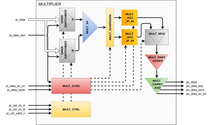
Electronics 2020, 9, 1141                                                                          2 of 20

•     Solving ill-conditioned linear systems of equations; many scientific problems involve
      ill-conditioned linear systems that give rise to numerical errors even when using 64-bit
      floating-point arithmetic.
•     Computing large sums; anomalous results often stem from the loss of associativity in summations,
      wrong order of summations or the usage of inadequate algorithms [9,10].
•     Executing long-time simulations; almost any kind of physical simulation (e.g., N–body
      simulations [11,12]) is sensitive to cumulative round-off errors, in addition to errors arising
      from discretization of time and space.
•     Executing large-scale simulations; computations that are well-behaved on modest-size problems
      may exhibit significant numerical errors when scaled up to massively parallel systems, because
      making numerical computations parallel is not trivial [12].
•     Resolving small-scale phenomena; very fine-scale resolutions can result in numerical problems.
•     ”Experimental mathematics” computations; numerous recent results in experimental mathematics
      could not be obtained without MPA computations.

      In our opinion, it is necessary also to add to this list other important MPA applications such as:

•     Generation of special mathematical functions applicable in scientific computations (e.g., discrete
      Green’s function (DGF), Bessel functions, etc.).
•     Cryptography and cryptanalysis.

      Unfortunatelly, MPA applications involve large computing resources, i.e., processor time
and memory consumption. According to [1], computations on central processing units (CPUs) in
double-double precision typically run 5–10 times slower than those implemented in 64-bit arithmetic.
The slowdown is at least 25 times for quad-double arithmetic, more than 100 times for 100-digit
arithmetic, and over 1000 times for 1000-digit arithmetic. This means that the development of a
parallel MPA accelerator is currently vitally important for scientists who need to apply MPA in
their computations.
      Ref. [13] presents an arithmetic unit for variable high-precision operands suitable for
reconfigurable computing. This unit cooperates with a host computer. While this is regarded as
a seminal solution, it only accelerates arithmetic operations (i.e., multiplication, division and square
root) and does not allow for execution of dedicated codes. In [14], hardware designs, arithmetic
algorithms, and software support are presented for a family of variable-precision, interval arithmetic
processors. The aim of such processors is to provide a programmer the ability to specify the precision
of computations, determine the accuracy of the results and, if desired, correct implicit errors in
finite-precision computations. Unfortunately, these processor designs are only specified and simulated
at the behavioural level, and no physical implementation has been made. In [15], a special-purpose
very large instruction word processor for variable-precision arithmetic is presented, which uses unified
hardware to implement various algebraic and transcendental functions. Its performance is obtained
by using the explicitly parallel nature of the very large instruction word and dynamically varying
the precision of intermediate computations. A prototype of that processor, as well as an accelerator,
are implemented in a field-programmable gate array (FPGA), which provides 5–37 times of speedup
compared with a software library. In [16,17], the development of a series of boards is reported,
which accelerate scientific computations requiring high precision. These boards consist of processing
elements, including a floating-point multiply unit and an addition unit, which form a single-instruction
multiple-data processor. Although these hardware solutions are 80–200 times faster than corresponding
software implementations, their computations are limited to quadruple, hexuple, and octuple precision
arithmetic. In [18–20], a variable-precision floating-point accelerator is proposed, based on a refined
version of the universal number (UNUM) type I format, for high-performance-computing servers. It is
implemented as a coprocessor of the RISC-V processor generated with the Rocket-chip generator [21].
This design is prototyped and validated on FPGA. In general, the FLOPS performance of this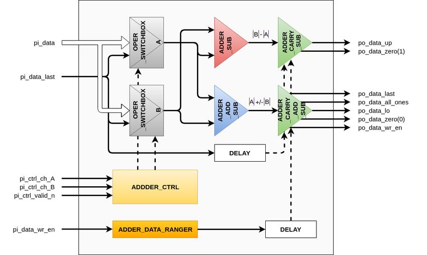
Electronics 2020, 9, 1141                                                                             3 of 20

architecture stays within the range of a regular fixed-precision IEEE floating-point unit. Furthermore,
the UNUM format allows interval arithmetic to be used in real applications having a variable
memory footprint.
       Up to now, none of the MPA processor/coprocessor results [13–20] presented in the literature
have gained either immense popularity or worldwide success. In our opinion, it stems partially from
the fact that none of those solutions are freely available as an open-source intellectual property (IP)
core. As a result, none of these solutions are available as a parallel computing coprocessor for MPA.
Despite the passage of time, the design of MPA processors/coprocessors remains an open scientific
problem, which we have also tried to solve [22–24]. Now, an MPA coprocessor is developed with
scalability, enabling its implementation in FPGAs of various scale using a single IP core. In this work,
the coprocessor is implemented on system on chip (SoC) devices (i.e., Zynq devices from Xilinx [25]),
but the design can also be implemented in FPGA PCIe accelerator cards. To the best of the Authors’
knowledge, this is the only recent integer MPA coprocessor which is both presented in the literature
and whose source code is available to the public.
       Recently, preliminary results have been reported from implementations of various MPA
operations [22,24] as well as the concept of the IP core for the integer MPA coprocessor [23]. In this
paper, a comprehensive and expanded report on this research is presented, delivering a significant
extension on the previous results. The new results in this paper focus on the acceleration of factorial (n!),
exponentiation (nn ) and DGF computations on Xilinx Zynq-7000 SoC. In all benchmarks, the integer
MPA coprocessor demonstrates advantages in terms of runtime in comparison with a CPU core
executing the same computations using a software MPA library. For sufficiently large input parameters,
our integer MPA coprocessor (implemented in FPGA on Zynq-7000 SoC) is up to three times faster
than a single CPU core within the same chip (ARM Cortex A9) emulating MPA using a software library.
It is important to state that the code of our coprocessor is open sourced and licensed under the Mozilla
Public License [26]. It can hopefully facilitate the investigations of other researchers who employ MPA,
because not only has the IP core of the MPA coprocessor been released but also the emulator and
benchmarking codes presented here.

2. Architecture of Coprocessor
      The very high speed integrated circuit hardware description language (VHDL) code of the
MPA coprocessor is developed for implementation in Xilinx Zynq-7000 SoC on TySOM-1 board from
Aldec [27] consisting of Kintex-7 architecture FPGA and two 32-bit ARM Cortex A9 CPU cores (package
XC7Z030-1FBG484C). The architecture of Zynq-7000 SoC with the MPA coprocessor is presented in
Figure 1. The processing system (PS) communicates with the programmable logic (PL) using an AXI
interface [28], requiring AXI interconnect and dedicated converters. In order to resolve the problem of
data integrity, the first-in first-out (FIFO) buffers are used for data storage and buffering between PS
and the MPA coprocessor. For the purpose of the coprocessor benchmarking in Section 4, the block
random access memory (BRAM) is connected to the MPA coprocessor through the AXI interface.
However, it can be removed in the target coprocessor configuration.
      Our aim is to develop an MPA coprocessor core that can be implemented in various FPGAs,
according to the required processing power of the final application. The IP core is parametrizable and
uses the sign-magnitude representation for integer numbers. This stems from the need to provide
an interface compatible with existing software codes and libraries employing MPA, such as the
GMP library [29], which is the standard software tool for implementation of MPA computations on
CPUs. Whilst the sign-magnitude representation of integer numbers is not so straightforward for
addition/subtraction implementation (requiring O(n) operations) as two’s complement representation,
it delivers time savings for the multiplication which requires O(n2 ) operations. The format of integer
numbers in our MPA coprocessor is presented in Figure 2. In our design, each number consists of a
header (64 bits) and data words (limbs) of 64 bits each. The header includes 9 bits of size (i.e., number
of limbs), 1 bit of a number sign and 3 bits of control flags for speeding-up processing on FPGA.
Electronics 2020, 9, 1141                                                                                                                                                                                        4 of 20

                            TySOM-1
                                                                                     DDR3                                                  PS

                                                                                                                                                                               SD,SPI,USB,UART, Ethernet, Hdmi
                                                                                    Controller

                                                                                                                                                    Peripherals Interconnect
                                                                                    525 MHz

                                    OCM Interconnect
                                                                                        L2                                               APU

                                                                                    Snoop                                         L1 ARM9
                                                             OCM
                                                                                    Control
                                                                                   Unit (SCU)                                     L1 ARM9
                                                                                     DMA                                                 PLL

                                                                                                             ACP AXI Master 64b
                                                                                   Controller                                          650 MHz
                                                                             Interconnect
                            HP0
                                  HP1
                                                HP2
                                                       HP3

                                                             MGP0
                                                                          MGP1

                                                                                       SGP0
                                                                                                  SGP1
                            AXI Masters                                                                                                             EMIO
                                64b                          AXI Masters Slaves 32b

                                                                                                                                    AXI BRAM
                                                                    AXI Interconnect
                                                                                                                                  (Result memory)
                                                              AXI to AXI Stream

                                                                                         AXI Stream to AXI
                                                                 Converters

                                                                                             Converter

                                                             FIFOs

                                                                     MPA
                                                                  Coprocessor
                                                                   400 MHz                                                                                                     PL

      Figure 1.   Architecture of Zynq-7000 SoC with implemented multiple-precision arithmetic
      (MPA) coprocessor.

                                  Figure 2. Format of integer numbers in MPA coprocessor.

     The overall diagram of our coprocessor is presented in Figure 3. In the basic configuration,
the coprocessor operates under control of host CPU. It exchanges data with host CPU using three 64-bit
data buses and a single 8-bit program bus. Two of the data buses (denoted as A and B) transfer data to
the coprocessor whilst the third-one transfers results of computations from the MPA coprocessor to
CPU. The buses are AMBA standard (AXI Stream) compliant [28]. There are 16 logical registers that
can be used in coprocessor codes. From the hardware point of view, those registers are mapped into
17 physical registers. One extra physical register is utilized for operations that may not produce an
Electronics 2020, 9, 1141 5 of 20
immediately unambiguous result. Extra result data is stored in it (e.g., during addition/subtraction
operation) and the proper result selection is made once the operation terminates. This additional
register is referred to as the shadow register. Whereas registers store magnitudes of MPA numbers,
their signs and sizes are stored in the control unit (CTRL). Loaders transfer data to the bank of registers
from data buses A and B whereas unloaders transfer data to CPU. Each register in the bank stores an
MPA number of the maximal length equal to 32 kbits. When instructions are fetched from the program
bus, they are decoded in the instruction decoder, then the control lines (Ctrl) are set accordingly to allow
data transfer from the registers to the multiplication and adder/subtractor units. Then, arithmetic
operations are executed and the results are transferred back to the bank of registers. The final results
of the MPA computations are transferred to CPU using the unloader module.
The control unit is responsible for fetching instructions for execution, instruction decoding,
and mapping register numbers from the logical representation given by the user to physical
representation in hardware. It executes instructions provided that all necessary resources are available,
otherwise it awaits them. When all resources required by the current operation are ready, the CTRL
unit generates appropriate control signals on the control lines. The control unit also monitors the
amount of individual resources, temporarily blocks or allows the next instruction to be executed,
and stores additional information supporting fast number processing.
Figure 3. Overall diagram of developed MPA coprocessor (MULT, ADD/SUB and CTRL denote
respectively multiplication, adder/subtractor and control units).
The instruction set includes fundamental arithmetic operations (i.e., addition, subtraction,
multiplication) as well as data loading instructions. The coprocessor design can be extended with
other operations (e.g., bit manipulation instructions) depending on the final user needs. The basic
instruction set is presented in Table 1.Electronics 2020, 9, 1141 6 of 20
Table 1. Basic instruction set of developed MPA coprocessor.
Instruction Result
loaa regX regX = data (busA)
loab regX regX = data (busB)
loaab regX, regY regX = data (busA) and regY = data (busB)
unl regX data (busO) = regX
mult regX, regY, regZ regZ = regX * regY
add regX, regY, regZ regZ = regX + regY
sub regX, regY, regZ regZ = regX − regY
regX, regY, regZ denote any of 16 registers of length 32 kbits. busA, busB, busO denote respectively bus A,
bus B and output bus.
Instructions loaa, loab, loaab load data to registers from data buses A and B. Instruction unl
transfers the value in a register to host CPU using the output data bus. Instructions mult, add, sub are
the arithmetic operations of multiplication, addition and subtraction. These instructions are similar
to standard processor arithmetic instructions. However, the coprocessor does not emulate MPA
operations calling external library functions. Hence, it does not need to perform program jumps and
memory operations (e.g., when the size of computation result is larger than the allocated memory) like
standard CPU with the MPA software library. However, when the size of the result of MPA operations
is larger than 32 kbits, there is an overflow, which has to be taken into account, usually during the
code development.
Although the proposed MPA coprocessor is presented as operating under the control of host CPU,
it can also be implemented in FPGA hardware as a self-contained, programmable device with its own
instruction set and data communication channels. That is, although the coprocessor can be managed
by host CPU, it only need streams of instructions and data. Hence, the proposed MPA coprocessor
can be a valuable solution for the acceleration of MPA computations, not only within SoC solutions
for embedded systems but also in other hardware realisations, e.g., FPGA PCIe accelerator cards.
Depending on required processing throughput, multiple instances of the MPA coprocessor can still
be implemented within a single chip. This flexibility is a vitally important feature of the presented
design. Furthermore, due to the implementation in FPGA, the presented MPA coprocessor is highly
energy efficient.
2.1. Multiplier Unit
Figure 4 shows a block diagram of the multiplier unit. It executes multiplication operations on
streamed data of absolute-value operands with the limb size set to 64 bits.
The sign of the result of the multiplication is determined in the control unit. The 64-bit bus pi_data
connects each of physical registers with the multiplier. The OPER_SWITCHBOX module selects data in
registers to be operands for multiplication operations. Data entering the multiplier are organized by
reading from the registers in an appropriate order, so as to obtain the final result ordered from the
least-significant to the most-significant limb in the shortest possible time. Then, the MULT_64 module
executes the multiplication operations of two 64 bit operands based on the basecase algorithm [29] to
give a 128 bit result. Hence, a series of partial results is obtained (each with the length set to two limbs),
which are transferred to two MULT_ACC_IP_64 accumulators, each of a single-limb size, with the use of
the MULT_DIVERSION demultiplexer. When the currently calculated limb of the result is ready in the
MULT_ACC_IP_64 module, it goes through the multiplexer MULT_MUX to the adder MULT_PART_ADDER.
Alongside this, the carry is transferred to the next limb. This adder is responsible for adding the limbs
with the corresponding carry transferred from the previous limb as well as returning a single limb
result and a carry. This data goes to the MULT_CARRY_ADD module, which is an adder of the number
and the carry, which allows for getting the final result.
In addition to the described modules, there are two local control modules that form control signals.
The MULT_CTRL module is responsible for reading information from the main control unit, decodingElectronics 2020, 9, 1141 7 of 20
it and starting the multiplication process. The MULT_SYNC module is responsible for forming control
signals so as to enable proper control (at the right time) of modules that process useful data.
Figure 4. Block diagram of multiplier unit.
2.2. Adder-Subtractor Unit
The adder-subtractor unit employs the sign-magnitude representation only for operands and
results [24]. Figure 5 presents its block diagram. Each of the ADDER_SUB and ADDER_ADD_SUB
blocks consist of two DSP48E1 modules [30] connected to form 64-bit precision modules enabling
addition and subtraction. These blocks generate a series of limbs with single-bit carries which are
transferred with the use of dedicated lines for DSP block communication.
The unit simultaneously computes two results, i.e., |B|−|A| and |A|+|B| in parallel using
ADDER_SUB and ADDER_ADD_SUB blocks in the case of addition and |B|−|A| and |A|−|B|
in the case of subtraction. There is no quick and easy way to determine in advance which operand
is greater, so the sign of the result is known only at the end of the addition/subtraction operation.
However, the result can be a negative number in two’s complement representation. In this case,
the result would have to be converted to the sign-magnitude representation which doubles the
processing time, i.e., the bits of the number would have to be inverted and one added to it. Therefore,
a double processing pipeline is used and operations are executed on absolute values of operands
as described above. In this method, both results are stored in registers (target logical register and
auxiliary shadow register) and finally one of them is taken as a valid result with a sign bit adjusted
accordingly. Based on the signs of input operands as well as both results of computations, the correct
value is taken whose two’s complement representation is the same as the magnitude of the result in
the sign-magnitude representation. For some cases, the logical number associated with the register
of the addition/subtraction output interchanges with the number of the shadow register. Table 2
presents the truth table for the addition operation, allowing us to correctly set the sign of the result as
well as the register storing a correct magnitude of the result. Table 3 presents the truth table for the
subtraction operation, allowing us to correctly set the sign of the result as well as the register storing
a correct magnitude of the result. Such logic functions are implemented within the designed digital
circuit. Our design avoids the conversion of addition and subtraction results from two’s complementElectronics 2020, 9, 1141 8 of 20
representation to the sign-magnitude representation but requires increased resources in terms of
logic cells.
Figure 5. Block diagram of adder-subtractor unit.
Table 2. Truth table allowing us to adjust sign and take corect register as result of addition [24].
Correct Result Result Sign
|A| vs. |B| A Sign B Sign Example Operations
Sign Sign Taken Change
ADDER_ADD_SUB: |A|+|B| + X
|A| > |B| A>0 B>0 5+2=7 + ×
ADDER_SUB: |B|−|A| − ×
ADDER_ADD_SUB: |A|−|B| + X
|A| > |B| A>0 B |B| A0 −5 + 2 = −3 − X
ADDER_SUB: |B|−|A| − ×
ADDER_ADD_SUB: |A|+|B| + X
|A| > |B| A0 3+3=6 + ×
ADDER_SUB: |B|−|A|= 0 + ×
ADDER_ADD_SUB: |A|−|B|= 0 + X
|A| = |B| A>0 B0 BElectronics 2020, 9, 1141 9 of 20
Table 3. Truth table allowing us to adjust sign and take corect register as result of subtraction [24].
Correct Result Result Sign
|A| vs. |B| A Sign B Sign Example Operations
Sign Sign Taken Change
ADDER_ADD_SUB: |A|−|B| + X
|A| > |B| A>0 B>0 5−2=3 + ×
ADDER_SUB: |B|−|A| − ×
ADDER_ADD_SUB: |A|+|B| + X
|A| > |B| A>0 B |B| A0 −5 − 2 = −7 − X
ADDER_SUB: |B|−|A| − ×
ADDER_ADD_SUB: |A|−|B| + X
|A| > |B| A0 3−3=0 + (0) ×
ADDER_SUB: |B|−|A|= 0 + ×
ADDER_ADD_SUB: |A|+|B| + X
|A| = |B| A>0 B0 BElectronics 2020, 9, 1141 10 of 20
proc_sys_reset_0
slowest_sync_clk mb_reset
axi_interconnect_2
ext_reset_in bus_struct_reset[0:0]
Axi2AxiStream_1
aux_reset_in peripheral_reset[0:0]
S00_AXI axis_data_fifo_1
mb_debug_sys_rst interconnect_aresetn[0:0]
ACLK S00_AXI
dcm_locked peripheral_aresetn[0:0]
ARESETN clk s_axis_mm2s S_AXIS
clk_wiz_0
S00_ACLK rstn s_axis_aresetn M_AXIS
Processor System Reset
S00_ARESETN s_axis_aclk
resetn clk_out1 M00_AXI
M00_ACLK Axi2AxiStream_v1_0
clk_in1 locked proc_sys_reset_1 M01_AXI
M00_ARESETN AXI4-Stream Data FIFO
M02_AXI S00_AX
M01_ACLK
Clocking Wizard slowest_sync_clk mb_reset M03_AXI S01_AX
M01_ARESETN
ext_reset_in bus_struct_reset[0:0] Axi2AxiStream_0 core_0 ACLK
M02_ACLK
aux_reset_in peripheral_reset[0:0] axis_data_fifo_0 ARESETN
M02_ARESETN
mb_debug_sys_rst interconnect_aresetn[0:0] S00_AXI s00_ctrl_axis AxiStream2Axi_0 S00_ACLK
M03_ACLK
dcm_locked peripheral_aresetn[0:0] clk s_axis_mm2s S_AXIS s00a_axis S00_ARES
M03_ARESETN
rstn s_axis_aresetn M_AXIS s00b_axis m00_axis m_axis_mm2s M00_ACLK
M00_AXI
Processor System Reset s_axis_aclk pi_clk clk M00_ARES
AXI Interconnect IRQ
Axi2AxiStream_v1_0 pi_rst rstn S01_ACLK
AXI4-Stream Data FIFO S01_ARES
core_v1_0 AxiStream2Axi_v1_0
sys_ps7
PTP_ETHERNET_0
DDR
FIXED_IO
UART_0 Axi2AxiStream_2
SDIO_0 axis_data_fifo_2
M_AXI_GP0_ACLK
SDIO0_CDN S00_AXI
IRQ_F2P[15:0]
SDIO0_WP clk s_axis_mm2s S_AXIS
USBIND_0 rstn s_axis_aresetn M_AXIS
M_AXI_GP0 s_axis_aclk
FCLK_CLK0 Axi2AxiStream_v1_0
FCLK_RESET0_N AXI4-Stream Data FIFO
ZYNQ7 Processing System
Figure 7. Data-flow diagram for operation of data-writing to MPA coprocessor.
The final result of the computations is sent by the MPA coprocessor to BRAM through the AXIS
master interface. For this purpose, the AXIS–AXI4 converter and the AXI interconnect block are used to
store data and share it with ARM Cortex A9. Figure 8 shows the data-flow diagram for the connection
axis_data_fifo_1
between the coprocessor and BRAM, where orange wires denote active AXI connections.
S_AXIS
s_axis_aresetn M_AXIS
s_axis_aclk
axi_interconnect_1
AXI4-Stream Data FIFO
S00_AXI
S01_AXI
core_0 ACLK
axi_bram_ctrl_0
axis_data_fifo_0 ARESETN axi_bram_ctrl_0_bram
s00_ctrl_axis AxiStream2Axi_0 S00_ACLK
M00_AXI S_AXI
S_AXIS s00a_axis S00_ARESETN BRAM_PORTA BRAM_PORTA
s_axi_aclk
s_axis_aresetn M_AXIS s00b_axis m00_axis m_axis_mm2s M00_ACLK BRAM_PORTB BRAM_PORTB
M00_AXI s_axi_aresetn
s_axis_aclk pi_clk clk M00_ARESETN
IRQ
pi_rst rstn S01_ACLK Block Memory Generator
AXI BRAM Controller
AXI4-Stream Data FIFO S01_ARESETN
core_v1_0 AxiStream2Axi_v1_0
AXI Interconnect
Figure 8. Data-flow diagram for data-writing operation to block random access memory (BRAM) from DDR
FIXED_IO
axis_data_fifo_2
MPA coprocessor.
S_AXIS GND
s_axis_aresetn
s_axis_aclk
M_AXIS
The MPA coprocessor is implemented in FPGA with the clock frequency equal to 400 MHz dout[0:0]
AXI4-Stream Data FIFO (less than the physical limit of 458 MHz for this FPGA). The time of the code execution on the MPA Constant
coprocessor is measured with the use of an additional timer triggered by the rising edge of the clock at
the beginning of the execution of the first code instruction. The end of computations is triggered by the
first transfer of resulting data (signal TVALID = 1 on AXIS master interface). The results of software
simulation and hardware verification are always consistent in terms of the number of clock cycles
in executed operations. Of course, obtained speedups of the MPA coprocessor against CPU depend
on the clock frequency. Such a design requires currently hardware resources as in Table 4, where the
resources are presented for the MPA coprocessor alone and with the infrastructure for communication
with host CPU. With the use of resources available on Zynq-7000 SoC, the implementation of six MPA
cores is possible in this chip assuming 80% utilization of FPGA resources.
The Aldec TySOM-1 board operates under the control of a Linux real-time operating system
(RTOS) with a hardware application layer (HAL) that supports AXI4 interface. The application is
developed based on HAL functions. It transfers a code to the MPA coprocessor and waits for the
result. However, the times measured in benchmarks do not include the read latency stemming from
data transfers between BRAM and the host processor through M_AXI_GP0 port. It is verified that the
communication between the MPA and host processors using the AXI interconnect does not introduce
significant overhead to the benchmarks presented below. That is, the measured time for writing
64 kbits of data (two MPA numbers of the maximal size) to the MPA coprocessor is equal to 0.18 µs.
Then, the measured time for reading 64 kbits of data from the MPA coprocessor is equal to 0.16 µs.
Hence, one can conclude when it is reasonable to use the proposed MPA coprocessor implemented onElectronics 2020, 9, 1141 11 of 20
Zynq-7000 SoC. That is, the communication overhead between CPU and FPGA has to be negligible in
comparison with the computation time on CPU using the MPA software library.
Table 4. Resources required for implementation of MPA coprocessor.
MPA Coprocessor Alone With Infrastructure
Resources Used Available Utilization (%) Used Available Utilization (%)
slice LUTs 8745 78,600 11.13 15,735 78,600 20.02
LUT as logic 8673 78,600 11.03 14,238 78,600 18.11
LUT as memory 72 26,600 0.27 1497 26,600 5.63
slice registers 16,249 157,200 10.34 27,708 157,200 17.63
register as flip flop 16,249 157,200 10.34 27,705 157,200 17.62
register as latch 0 157,200 0 3 157,200Electronics 2020, 9, 1141 12 of 20
1200
MPA coprocessor
ARM Cortex A9
1000
800
time ( sec)
600
400
200
0
100 200 300 400 500 600 700 800 900 1000
n
Figure 9. Runtimes for factorial computations (n!).
4.2. Computations of Exponentiation
In Table 6, listing of the code for n-th power of n computations is presented for n = 4. In line 1,
reg0 and reg1 are loaded with initial data equal to n = 4. Then (line 2), value of reg2 is obtained by
multiplying reg0 and reg1 (reg0 = reg1 = n = 4). In the next line (line 3), reg2 is multiplied by reg1 and
result is stored in reg0 (reg2 = 16). Then (line 4), value of reg2 is obtained by multiplying reg0 and reg1
(reg2 = 256). Finally, value of reg2 is unloaded in line 5.
Table 6. Listing of code for n-th power of n computations (n = 4).
Line Instruction
1 loaab reg0, reg1;
2 mult reg0, reg1, reg2;
3 mult reg2, reg1, reg0;
4 mult reg0, reg1, reg2;
5 unl reg2;
reg0, reg1 are initially loaded with n.
In Figure 10, measured runtimes for the MPA coprocessor and the ARM Cortex A9 core are
presented for n-th power of n (nn ) computations for n varying in the range approaching n = 1000.
To compute nn for n = 1000, a single core of an ARM Cortex A9 processor needs 1267 µs whereas
the MPA coprocessor needs 366 µs. In this test, the developed MPA coprocessor is 3.46 times faster
than a single core of ARM A9 processor within the same SoC.Electronics 2020, 9, 1141 13 of 20
1400
MPA coprocessor
ARM Cortex A9
1200
1000
time ( sec)
800
600
400
200
0
100 200 300 400 500 600 700 800 900 1000
n
Figure 10. Runtimes for n-th power of n computations (nn ).
4.3. Computations of DGF
The MPA coprocessor is benchmarked in computations of the one-dimmensional (1-D) scalar DGF
in electromagnetics [2–5,32]. This function allows one to represent 1-D finite-difference time-domain
(FDTD) update equations [32,33] with the use of the convolution formulation
−n0 −n0
" # " # " 0 #
Ekn Gee nk− Geh nk− Jkn0
Hkn
= ∑0 0 G
k0
n−n0
Ghh k−k0
k0 ·
n−n0 Mkn0
0 (1)
nk he k −k0
where E and H denote, respectively, electric- and magnetic-field vectors, J and M denote, respectively,
electric- and magnetic-current source vectors, and n and k denote, respectively, temporal and spatial
indices of the 1-D FDTD grid. Gee , Geh , Ghe , Ghh functions can be obtained for a free space as follows:
∆t n
Gee nk = − gk − gkn−1
e0
Geh k = ∆zγ2 gkn − gkn−1
n
Ghe nk = ∆zγ2 gkn+1 − gkn
∆t n+1
Ghh nk = − gk − gkn (2)
µ0
where e0 and µ0 denote, respectively, permittivity and permeability of the free space, and ∆t and ∆z
denote, respectively, temporal- and spatial-step sizes. 1-D scalar DGF is computed with the use of the
following formula:
n −1
m+n 2m
gkn = ∑ γ2m (−1)m+k (3)
m=k
2m + 1 m + kElectronics 2020, 9, 1141 14 of 20
√
where γ = c∆t
∆z (c = 1/ µ0 e0 ) denotes the Courant number that must be less than or equal to one
(γ ≤ 1) to guarantee the stability of computations. The implementation of (3) in software requires
MPA [2]. Let us assume γ = 1 because a simple formula for scalar DGF computations (provable by the
mathematical induction [32]) exists in this case
0, n ≤ k
gkn = 0, n > k and (n + k) even . (4)
1, n > k and (n + k) odd
Hence, 1-D scalar DGF is computed in our benchmark with the use of (3) for γ = 1 and the
correctness of the computations is verified with the use of (4). In the codes, binomial coefficients are
loaded from memory in order resulting from the sum in (3). Thus, only the computational throughput
in multiplication and addition/subtraction of MPA numbers is measured in this benchmark.
In Table 7, listing of the code for DGF computations is presented for n = 4 and k = 0. In line 1,
reg4 is loaded with 0. Then (line 2), reg0 and reg1 are loaded with 4 and 1, respectively. Then (line
3), value of reg2 is obtained by multiplying reg0 and reg1. In the next line (line 4), reg4 is added to
reg2 and result is stored in reg3. Then (line 5), reg0 and reg1 are loaded with 10 and 2, respectively.
Then (line 6), value of reg2 is obtained by multiplying reg0 and reg1. In the next line (line 7), reg2 is
subtracted from reg3 and result is stored in reg4. Then (line 8), reg0 and reg1 are both loaded with 6.
Then (line 9), value of reg2 is obtained by multiplying reg0 and reg1. In the next line (line 10), reg4 is
added to reg2 and the result is stored in reg3. Then (line 11), reg0 and reg1 are loaded with 1 and 20,
respectively. Then (line 12), value of reg2 is obtained by multiplying reg0 and reg1. In the next line
(line 13), reg2 is subtracted from reg3 and result is stored in reg4 (reg4 = 0). Finally, value of reg4 is
unloaded in line 14.
Table 7. Listing of code for discrete Green’s function (DGF) computations (n = 4, k = 0).
Line Instruction
1 loaa reg4;
2 loaab reg0, reg1;
3 mult reg0, reg1, reg2;
4 add reg4, reg2, reg3;
5 loaab reg0, reg1;
6 mult reg0, reg1, reg2;
7 sub reg3, reg2, reg4;
8 loaab reg0, reg1;
9 mult reg0, reg1, reg2;
10 add reg4, reg2, reg3;
11 loaab reg0, reg1;
12 mult reg0, reg1, reg2;
13 sub reg3, reg2, reg4;
14 unl reg4;
Line 1: reg4 is loaded with 0. Line 2: reg0, reg1 are respectively loaded with 4 and 1. Line 5: reg0, reg1
are respectively loaded with 10 and 2. Line 8: reg0, reg1 are both loaded with 6. Line 11: reg0, reg1 are
respectively loaded with 1 and 20.
In Figure 11, measured runtimes for the MPA coprocessor and the ARM Cortex A9 core are
presented for k = 0 and k = 99 with n varying in the range approaching 2000. To compute DGF
for n = 2000 and k = 0 (k = 99), a single core of ARM A9 processor needs 57,254 µs (56,416 µs)
whereas the MPA coprocessor needs 5529.8 µs (5446.3 µs). For these parameters, the developed MPA
coprocessor is around 10.35 times faster than a single core of ARM A9 processor within the same SoC.
For the MPA coprocessor, the DGF computation time can be estimated as
−1
t DGF = Anα f clk . (5)Electronics 2020, 9, 1141 15 of 20
With the use of regression for n ≥ 1000, A = 0.0046, α = 2.6287 and A = 0.0028, α = 2.6908 are
obtained for k = 0 and k = 99, respectively. For the considered design, the clock frequency f clk is set to
400 MHz.
104
6
MPA coprocessor (k=0)
ARM Cortex A9 (k=0)
5 MPA coprocessor (k=99)
ARM Cortex A9 (k=99)
4
time ( sec)
3
2
1
0
0 200 400 600 800 1000 1200 1400 1600 1800 2000
n
Figure 11. Runtimes for DGF computations. MPA coprocessor results overlap for k = 0 and k = 99.
To sum up the results, the developed coprocessor is benchmarked in factorial, exponentiation
and DGF computations. In factorial and exponentiation computations, the coprocessor (implemented
in FPGA on SoC) can be three times faster than a single CPU core within the same chip. In the
task of DGF generation, the MPA coprocessor is more than ten times faster than a single CPU core
within the same chip. The obtained difference between the speedups for factorial/exponentiation
and DGF computations is due to the structure of the DGF code. The difference depends on the
amount of data retrieved from the processor memory. The ARM Cortex A9 processor can perform
short computations using L1 cache when code jumps do not exceed its size. This is the case with the
ARM Cortex A9 equipped with 32 KB L1 cache, hence these operations are carried out quickly
in factorial/exponentiation computations. When computations make it impossible to enter the
pipeline, numerous jumps in memory are executed as in the case of DGF computations. Then,
the cache size is insufficient to optimize the code execution and the ARM Cortex A9 performance
decreases compared to the MPA coprocessor, which has a dedicated architecture of long registers and
pipelined data processing. Hence, the MPA coprocessor does not execute program loops, memory
operations and does not call external MPA library functions, which slow down CPU. It is verified in
simulation that the ratio of the total execution time of arithmetic operations to the total time of the
code execution approaches 99% for the factorial and exponentiation computations (n = 1000). In the
DGF computations, this coefficient is equal to 96% and 98% for n = 1000 and n = 2000, respectively.
It confirms the efficient implementation of the data processing in the MPA coprocessor. Hence, further
improvements in the coprocessor design can be obtained using faster arithmetic units. However,Electronics 2020, 9, 1141 16 of 20
the dedicated coprocessor for integer MPA computations is not as flexible a computational unit as
CPU. Furthermore, operand sizes for MPA operations are limited up to 32 kbits in our design. It is
worth noticing that ARM cores are hard-core processors, whereas the MPA coprocessor is implemented
within the programmable logic. Hence, FPGA within SoC can still be reprogrammed to implement
various logic functions, depending upon user needs. Furthermore, it is still possible to implement
several MPA cores within SoC, allowing for flexible reconfigurable parallel computing.
5. Materials and Methods
The Vivado Design Suite from Xilinx [31] is employed as a software tool for the design of the
presented MPA coprocessor. In the design process, simulation waveforms are obtained with the use of
Aldec Riviera tool [34]. The MPA coprocessor is implemented in Xilinx Zynq-7000 SoC on TySOM-1
board from Aldec [27]. The benchmarking setup for the MPA coprocessor is presented in Figure 12,
whereas the picture of the benchmarking hardware is presented in Figure 13. The benchmarking
codes can be executed either on CPU or FPGA. Then, the external host computer is used to manage
benchmarks and acquire execution times. The reference CPU codes are executed on ARM Cortex A9
on TySOM-1 board, which operates under the control of Linux RTOS (i.e., PetaLinux) loaded from
an SD card. Runtimes are measured on CPU using the system clock. In order to measure runtimes
on FPGA, the external host computer communicates with the integrated logic analyser (ILA) [35]
within FPGA using JTAG interface. ILA is implemented within FPGA as an IP core and is used to
monitor internal signals and registers of a design. As mentioned, the time of the code execution is
measured on the MPA coprocessor with the use of timer. This timer is triggered by the rising edge of
the clock at the beginning of the execution of the first code instruction whilst the end of computations
is triggered by the first transfer of resulting data. A value in the timer is acquired using ILA and
transferred then to the host computer. The entire process of receiving results is handled from the level
of Xilinx Vivado tool (i.e., Program & Debug tab). The results are downloaded using the JTAG server
working as “daemon tool” and placed on time charts of the signal state analyser. The results presented
in Figures 9–11 are taken for the values of the parameter n, which allow us to process the measurement
results within a reasonable time.
The results for ARM Cortex A9 are obtained using CPU codes compiled with the use of the
GNU CC compiler (version 4.9.2, disabled all optimizations). The following compilation options were
additionally considered for the code optimization on CPU: -O2, -O3, -Ofast, -Os, -Og. These options
allow us to speed up the code execution, reduce the code size as well as support the code debugging.
In comparison to the compilations with disabled all optimizations, runtimes are maximally reduced
by 5% for computations of factorials and n-th power of n (n ≥ 200), whereas runtimes are maximally
reduced by 3% for DGF computations (n ≥ 300). Therefore, the results are presented for the CPU
codes compiled with all optimizations disabled.
The design flow of the developed MPA coprocessor is presented in Figure 14. Based on the
design requirements, the development of the coprocessor architecture and test environment start
simultaneously. Afterwards, basic blocks (i.e, multiplier, adder-subtractor, registers, etc.) are developed
which are then integrated into the coprocessor. The developed coprocessor codes are tested in
behavioural simulations (using VHDL codes) and functional simulations (using SystemVerilog (SV)
and C codes). Afterwards, the coprocessor is benchmarked in simulations and its performance is
compared to the ARM Cortex A9 core with the GMP library. The feedback from the design process
allows us to modify the design to obtain the design requirements. Finally, the MPA coprocessor is
verified and benchmarked on hardware.Electronics 2020, 9, 1141 17 of 20
TySOM-1
Root FS
PS
SD,SPI,USB,UART, Ethernet, Hdmi
DDR3
Peripherals Interconnect
Linux Kernel
Device Tree SD
Controller
Bit Stream 525 MHz
uBoot
ARM9 Petalinux
ARM9 Benchmark
DMA PLL
UART
Controller 650 MHz
Interconnect
MGP0
MGP1
SGP0
SGP1
AXI Masters Slaves 32b EMIO
PL
USB UART Terminal AXI BRAM
AXI Interconnect
(Result memory)
AXI to AXI Stream
AXI Stream to AXI
Converters
Converter
Tvalid
Start Tready
Host Computer
Linux OS Timer Tvalid
Tready
Stop
FIFOs
Xilinx Vivado MPA
Program & Debug Xilinx Platform
Cable USB II
ILA Coprocessor Benchmark
JTAG Server 400 MHz
Figure 12. Benchmarking setup for MPA coprocessor.
Figure 13. Picture of benchmarking hardware for MPA coprocessor.Electronics 2020, 9, 1141 18 of 20
Design Requirements
Test Environment
Architectural Design
Design
VHDL Behavioural Simulations
Basic Block Design
/Multiplier, Adder-Subtractor,
Registers, etc./ SV/C
Functional Simulations
VHDL Behavioural Simulations
Integration of Blocks
into
MPA Coprocessor SV/C
Functional Simulations
Direct
Coprocessor Benchmarking Comparison
in
Simulations
ARM A9
Benchmarking
in
MPA Computations
Direct
Verification and Benchmarking Comparison
in
Hardware
IP Core
of
MPA Coprocessor
Figure 14. Design flow of MPA coprocessor.
6. Conclusions
Our open-source coprocessor is intended to support MPA computations by offloading them from
the CPU, with precision varying in the range between 64 bits and 32 kbits, with the limb size set to
64 bits. In our solution, MPA numbers are stored with the use of the sign-magnitude representation
to increase efficiency of the multiplication operation as well as to enable compatibility with existing
software MPA libraries. The developed coprocessor is benchmarked in factorial, exponentiation and
DGF computations, using an FPGA implementation on Xilinx Zynq-7000 SoC on TySOM-1 board
from Aldec. In the factorial and exponentiation benchmarks, our coprocessor can be three times faster
than a single CPU core within the same chip for sufficiently large input parameters. In the task of
DGF generation, the MPA coprocessor is more than ten times faster than a single CPU core within
the same chip for sufficiently large input parameters. With no more than 80% resource utilization,
one can implement six MPA cores on Zynq-7000 SoC. The speedup is obtained as a result of aggressive
optimization of performance and resource consumption. It means that over 87% of the maximum
operating frequency is obtained for the bottleneck element in FPGA (BRAM), whose maximum
operating frequency is equal to 458 MHz. It is clearly demonstrated that the embedding of MPA
computations in programmable logic within SoC is an attractive direction for the future development
of MPA computations accelerator. Our MPA coprocessor can facilitate other researchers involved in
MPA scientific computing, because the VHDL code of the MPA coprocessor is open-sourced, along
with all emulation and benchmarking codes presented in this paper. The next steps of this work are toElectronics 2020, 9, 1141 19 of 20
develop a bit manipulation unit, apply the coprocessor for data encryption, and integrate it with the
RISC-V processor.
Author Contributions: Conceptualization, K.R. and T.P.S.; methodology, K.R. and T.P.S.; firmware and software,
K.R. and T.P.S.; validation, K.R., T.P.S. and W.Ż.; investigation, K.R., T.P.S. and W.Ż.; data curation, W.Ż.;
writing—original draft preparation, K.R., T.P.S. and W.Ż.; writing—review and editing, K.R., T.P.S. and W.Ż.
All authors have read and agreed to the published version of the manuscript.
Funding: This research received no external funding.
Acknowledgments: Tomasz Stefański is grateful to Cathal McCabe at Xilinx Inc. for arranging the donation of
design software tools.
Conflicts of Interest: The authors declare no conflict of interest.
References
1. Bailey, D.; Barrio, R.; Borwein, J. High-precision computation: Mathematical physics and dynamics.
Appl. Math. Comput. 2012, 218, 10106–10121. [CrossRef]
2. Stefański, T.P. Electromagnetic Problems Requiring High-Precision Computations. IEEE Antennas Propag.
Mag. 2013, 55, 344–353. [CrossRef]
3. Stefanski, T.P. Fast Implementation of FDTD-Compatible Green’s Function on Multicore Processor.
IEEE Antennas Wirel. Propag. Lett. 2012, 11, 81–84. [CrossRef]
4. Stefański, T.P.; Krzyzanowska, K. Implementation of FDTD-Compatible Green’s Function on Graphics
Processing Unit. IEEE Antennas Wirel. Propag. Lett. 2012, 11, 1422–1425. [CrossRef]
5. Stefanski, T.P. Implementation of FDTD-Compatible Green’s Function on Heterogeneous Cpu-GPU Parallel
Processing System. Prog. Electromagn. Res. 2013, 135, 297–316. [CrossRef]
6. Ergül, Ö.; ı şcan Karaosmanoğlu, B. Low-Frequency Fast Multipole Method Based on Multiple-Precision
Arithmetic. IEEE Antennas Wirel. Propag. Lett. 2014, 13, 975–978. [CrossRef]
7. Kalfa, M.; Ergül, Ö; Ertürk, V.B. Error Control of Multiple-Precision MLFMA. IEEE Trans. Antennas Propag.
2018, 66, 5651–5656. [CrossRef]
8. Kalfa, M.; Ertürk, V.B.; Ergül, Ö. Error Control of MLFMA within a Multiple- Precision Arithmetic
Framework. In Proceedings of the 2018 IEEE International Symposium on Antennas and Propagation
USNC/URSI National Radio Science Meeting, Boston, MA, USA, 8–13 July 2018; pp. 2299–2300.
9. Wolfe, J.M. Reducing Truncation Errors by Programming. Commun. ACM 1964, 7, 355–356. [CrossRef]
10. Kahan, W. Pracniques: Further Remarks on Reducing Truncation Errors. Commun. ACM 1965, 8, 40
[CrossRef]
11. Goodman, J.; Heggie, D.C.; Hut, P. On the Exponential Instability of N-Body Systems. Astrophys. J. 1993,
415, 715. [CrossRef]
12. Gustafson, J. The End of Error: Unum Computing; CRC Press: Boca Raton, FL, USA, 2017.
13. Tenca, A.F.; Ercegovac, M.D. A variable long-precision arithmetic unit design for reconfigurable coprocessor
architectures. In Proceedings of the IEEE Symposium on FPGAs for Custom Computing Machines (Cat.
No.98TB100251), Napa Valley, CA, USA, 17 April 1998; pp. 216–225. [CrossRef]
14. Schulte, M.J.; Swartzlander, E.E. A family of variable-precision interval arithmetic processors. IEEE Trans.
Comput. 2000, 49, 387–397. [CrossRef]
15. Lei, Y.; Dou, Y.; Guo, S.; Zhou, J. FPGA Implementation of Variable-Precision Floating-Point Arithmetic.
In Advanced Parallel Processing Technologies; Temam, O., Yew, P.C., Zang, B., Eds.; Springer: Berlin/Heidelberg,
Germany, 2011; pp. 127–141.
16. Daisaka, H.; Nakasato, N.; Makino, J.; Yuasa, F.; Ishikawa, T. GRAPE-MP: An SIMD Accelerator Board for
Multi-precision Arithmetic. Procedia Comput. Sci. 2011, 4, 878–887. [CrossRef]
17. Daisaka, H.; Nakasato, N.; Ishikawa, T.; Yuasa, F. Application of GRAPE9-MPX for High Precision
Calculation in Particle Physics and Performance Results. Procedia Comput. Sci. 2015, 51, 1323–1332.
[CrossRef]
18. Bocco, A.; Durand, Y.; De Dinechin, F. SMURF: Scalar Multiple-Precision Unum Risc-V Floating-Point
Accelerator for Scientific Computing. In CoNGA’19, Proceedings of the Conference for Next Generation Arithmetic
2019; Association for Computing Machinery: New York, NY, USA, 2019. [CrossRef]Electronics 2020, 9, 1141 20 of 20
19. Bocco, A.; Durand, Y.; de Dinechin, F. Dynamic Precision Numerics Using a Variable-Precision UNUM Type
I HW Coprocessor. In Proceedings of the 2019 IEEE 26th Symposium on Computer Arithmetic (ARITH),
Kyoto, Japan, 10–12 June 2019; pp. 104–107.
20. Bocco, A.; Jost, T.T.; Cohen, A.; de Dinechin, F.; Durand, Y.; Fabre, C. Byte-Aware Floating-point Operations
through a UNUM Computing Unit. In Proceedings of the 2019 IFIP/IEEE 27th International Conference on
Very Large Scale Integration (VLSI-SoC), Cuzco, Peru, 6–9 October 2019; pp. 323–328.
21. Asanović, K.; Avizienis, R.; Bachrach, J.; Beamer, S.; Biancolin, D.; Celio, C.; Cook, H.; Dabbelt, D.; Hauser, J.;
Izraelevitz, A.; et al. The Rocket Chip Generator; Technical Report UCB/EECS-2016-17; EECS Department,
University of California: Berkeley, CA, USA, 2016.
22. Rudnicki, K.; Stefański, T.P. FPGA implementation of the multiplication operation in multiple-precision
arithmetic. In Proceedings of the 2017 MIXDES—24th International Conference Mixed Design of Integrated
Circuits and Systems, Bydgoszcz, Poland, 22–24 June 2017; pp. 271–275. [CrossRef]
23. Rudnicki, K.; Stefanski, T.P. IP Core of Coprocessor for Multiple-Precision-Arithmetic Computations.
In Proceedings of the 2018 25th International Conference Mixed Design of Integrated Circuits and System
(MIXDES), Gdynia, Poland, 21–23 June 2018; pp. 416–419. [CrossRef]
24. Rudnicki, K.; Stefanski, T.P. Implementation of Addition and Subtraction Operations in Multiple Precision
Arithmetic. In Proceedings of the 2019 26th International Conference Mixed Design of Integrated Circuits
and System (MIXDES), Rzeszów, Poland, 27–29 June 2019.
25. Xilinx Inc. Zynq-7000 All Programmable SoC Data Sheet: Overview—Product Specification. 2017.
Available online: www.xilinx.com (accessed on 8 August 2019).
26. Rudnicki, K.; Stefański, T.P.; Żebrowski, W. Integer-MPA-Coprocessor. 2020. Available online: https:
//github.com/stafan26/integer-MPA-coprocessor (accessed on 13 July 2020).
27. Aldec Inc. TySOM-1-7Z030—Technical Specification, Revision 1.7. 2017. Available online: www.aldec.com
(accessed on 8 August 2019).
28. Xilinx Inc. Vivado Design Suite—AXI Reference Guide, UG1037 (v4.0). 2017. Available online: www.xilinx.
com (accessed on 8 August 2019).
29. Granlund, T.; GMP Development Team. The GNU Multiple Precision Arithmetic Library (Edition 6.1.2).
2016. Available online: www.gmplib.org (accessed on 8 August 2019).
30. Xilinx Inc. 7 Series DSP48E1 Slice—User Guide, UG479 (v1.10). 2018. Available online: www.xilinx.com
(accessed on 8 August 2019).
31. Xilinx Inc. Vivado Design Suite User Guide—Getting Started, UG910 (v2018.3). 2018. Available online:
www.xilinx.com (accessed on 8 August 2019).
32. Gulgowski, J.; Stefański, T.P. Recurrence scheme for FDTD-compatible discrete Green’s function derived
based on properties of Gauss hypergeometric function. J. Electromagn. Waves Appl. 2019, 33, 637–653.
[CrossRef]
33. Taflove, A.; Hagness, S.C. Computational Electrodynamics: The Finite-Difference Time-Domain Method, 3rd ed.;
Artech House: Norwood, MA, USA, 2005.
34. Aldec Inc. Riviera-PRO Manual. 2017. Available online: www.aldec.com (accessed on 8 August 2019).
35. Xilinx Inc. Integrated Logic Analyzer v6.2—LogiCORE IP Product Guide, PG172. 2016. Available online:
www.xilinx.com (accessed on 8 August 2019).
© 2020 by the authors. Licensee MDPI, Basel, Switzerland. This article is an open access
article distributed under the terms and conditions of the Creative Commons Attribution
(CC BY) license (http://creativecommons.org/licenses/by/4.0/).You can also read