PRODUCT MANUAL LBC-LX800-G - AMD Geode 500 MHz Single Board Computer - WinSystems
←
→
Page content transcription
If your browser does not render page correctly, please read the page content below
WinSystems
                                                   ®

 LBC-LX800-G
 AMD Geode 500 MHz Single Board Computer

 PRODUCT MANUAL

                  y
              ar
      in
    im
  el
Pr

                       WinSystems, Inc.
                       715 Stadium Drive
                       Arlington, TX 76011

                       http://www.winsystems.com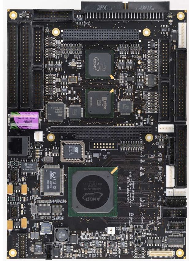
MANUAL REVISION HISTORY
P/N G400-0372-000B

 Revision Date Code   ECO Number
 111219

                                         y
                                    ar
                            in
                          im
                 el
               Pr

111219 PRODUCT MANUAL LBC-LX800-G 
TABLE OF CONTENTS
BEFORE YOU BEGIN	                                                      6
Visual Index - Top View (Connectors) 	                                 7
Visual Index - Top View (Jumpers & LEDs) 	                             8
Visual Index - Bottom View	                                            9
Jumper Reference	                                                     10

INTRODUCTION	                                                         14

FEATURES	                                                             14
    System	                                                           15
    Memory	                                                           15

FUNCTIONALITY	                                                        16
    I/O Port Map	                                                     16
    Interrupt Map	                                                    18
    Watchdog Timer	                                                   20

                                                 y
    Real-Time Clock/Calendar	                                         21

                                              ar
CONNECTOR REFERENCE	                                                  22
POWER	                                                                22
     J2 - AT Power	                                                   22
                                  in
     J30 - Push Button Reset (OEM Only)	                              22
                                im
BATTERY BACKUP	                                                       23
     J44 - External Battery	                                          23

VIDEO	                                                                24
                  el

     J1 - TTL Flat Panel	                                             24
     J5 - LVDS Flat Panel	                                            24
     J6 (CRT), J7 (CRT Legacy)	                                       25
                Pr

     J3 - Backlight Power	                                            26
     J9 - Backlight Inverter (OEM Only)	                              26
     J8 - Touchscreen Power (OEM Only)	                               26
     J10 - Flat Panel Power (OEM Only)	                               26
     J13 - Digital Flat Panel	                                        27
     J19 - Flat Panel Configuration	                                  27
     J21 - Backlight Power	                                           28
     J22 - Backlight Dimmer Switch	                                   28
     J23 - Backlight Control Selection	                               28

MOUSE	                                                                29
     J16 - Mouse	                                                     29

PARALLEL ATA	                                                         30
     J4 - PATA	30

PC/104 BUS	                                                           31
     J31, J33 - PC/104	31

COMPACTFLASH	                                                         32
     J101 - CompactFlash	32

111219 PRODUCT MANUAL LBC-LX800-G 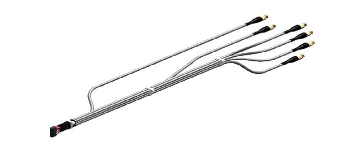
AUDIO	                                                         33
     J49 - Audio	33
     J42 - CD Input (OEM Only)	33
     SP1 - Speaker	33
USB	                                                           34
     J51, J52 - USB	34

ETHERNET	                                                      35
     J50 - Gigabit Ethernet	35

DIGITAL I/O	                                                   36
     J47, J53 - Digital I/O	36
     J48- Digital I/O Power	36

MULTI-I/O	                                                     37
     J28 - Multi-I/O (COM1, COM2, Keyboard, LPT)	37

SERIAL	                                                        39
     J37 - COM3, COM4	39

                                           y
     J12 - (COM5, COM6); J46 (COM7, COM8)	    41
     J11 - (COM9, COM10); J45 (COM11, COM12)	 43

                                      ar
     Register Definitions (WS16C48)	          45
     Register Details	        in              45

PC/104-Plus BUS	                                               47
     J34 - PC/104-Plus                                         47
                             im
BIOS SETTINGS STORAGE OPTIONS	                                 71
CABLES	                                                        73
SOFTWARE DRIVERS	                                              74
                  el

SPECIFICATIONS	                                                75
MECHANICAL DRAWING - TOP VIEW	                                 76
MECHANICAL DRAWING - BOTTOM VIEW	                              77
                Pr

APPENDIX - A	                                                  78
    BEST PRACTICES	                                            78
WARRANTY INFORMATION	                                          82

111219					                  PRODUCT MANUAL LBC-LX800-G
This page has been left intentionally blank.
y
ar
in
im
el
Pr
111219 PRODUCT MANUAL LBC-LX800-G BEFORE YOU BEGIN
WinSystems offers best practice recommendations for using and handling WinSystems embedded PCs. These methods
include valuable advice to provide an optimal user experience and to prevent damage to yourself and/or the product.
YOU MAY VOID YOUR WARRANTY AND/OR DAMAGE AN EMBEDDED PC BY FAILING TO COMPLY WITH THESE
BEST PRACTICES.
Reference Appendix - A for Best Practices.
Please review these guidelines carefully and follow them to ensure
you are successfully using your embedded PC.
This product ships with a heat sink. Product warranty is void if the
heat sink is removed from the product.
y
For any questions you may have on WinSystems products, contact our Technical Support Group at (817) 274-7553, Monday
through Friday, between 8 AM and 5 PM Central Standard Time (CST).
ar
in
im
el
Pr
111219 PRODUCT MANUAL LBC-LX800-G Visual Index - Top View (Connectors)
J28
J46 J37 Multi-I/O J34
COM7/COM8 COM3/COM4 (COM1/2, Keybd, PC/104-Plus
LPT)
J45
COM11/COM12
J47 J2
Digital I/O AT Power
(Ports D/E/F)
J4
J53 PATA
Digital I/O
(Ports A/B/C)
J12
COM5/COM6
y
J31 J11
ar
PC/104 (C/D) COM9/COM10
J33 J16
PC/104 (A/B)
in PS/2 Mouse
J44
im
External J1
Battery TTL Flat Panel
J10
Flat Panel Power
el
(OEM Only)
J50
Ethernet J9
Pr
Backlight
Inverter
(OEM Only)
J52
USB J3
(2/3) Backlight Power
J51 J8
USB Touchscreen
(0/1) Power
(OEM Only)
J6
CRT
J7
CRT (Legacy)
J42 J30
SP1 J49 J13 J5
CD Audio In PBRESET
Speaker Audio Digital Flat Panel Flat Panel
(OEM Only) (OEM Only)
RESERVED - J26, J27, J32
NOTE: The reference line to each component part has been drawn to Pin 1, and is also highlighted with a square, where applicable.
111219 PRODUCT MANUAL LBC-LX800-G Visual Index - Top View (Jumpers & LEDs)
J48 J36 J35 J29 J24
Digital I/O COM3 COM4 COM2 COM1
Power Termination Termination Termination Termination
J18
COM5
Termination
J17
J41 COM6
COM8 Termination
Termination
J40
COM7 J20
Termination CompactFlash
(Master/Slave)
y
J39
COM12
Termination
ar
J38 J15
COM11 COM9
Termination Termination
in
J14
COM10
Termination
im
J43
CMOS Battery
Enable
el
J25
Pr
Multi
Configuration
Selection
J23
Backlight Control
Selection
J22
Backlight
Dimmer
J21
Backlight Power
J19
Flat Panel
Configuration
RESERVED - J26, J27, J32
NOTE: The reference line to each component part has been drawn to Pin 1, and is also highlighted with a square, where applicable.
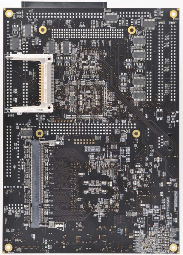
111219 PRODUCT MANUAL LBC-LX800-G Visual Index - Bottom View
J101
CompactFlash
y
ar
in
im
J102
Memory
el
Pr
RESERVED - J26, J27, J32
NOTE: The reference line to each component part has been drawn to Pin 1, and is also highlighted with a square, where applicable.
111219 PRODUCT MANUAL LBC-LX800-G Jumper Reference
NOTE: Jumper Part# SAMTEC 2SN-BK-G is applicable to all jumpers. These are available in a ten piece kit from
WinSystems (Part# KIT-JMP-G-200).
J20 - CompactFlash
J20
CompactFlash Master (default) 1-2
3 □
CompactFlash Slave 2-3
2 □
1 □
J24 - COM1, J29 - COM2, J36 - COM3, J35 - COM4, J18 - COM5, J17 - COM6
J40 - COM7, J41 - COM8, J15 - COM9, J14 - COM10, J38 - COM11, J39 - COM12
Termination Resistors Termination Resistors
COM1 = J24 COM3 = J36 COM5 = J18 COM9 = J15
COM2 = J29 COM4 = J35 COM6 = J17 COM10 = J14
1 □ □ 2
y
2 4 6 8
□ □ □ □ 3 □ □ 4
□ □ □ □ 5 □ □ 6
ar
1 3 5 7 7 □ □ 8
Termination Resistors RS-422 Termination and Biasing Resistors
TX (100): Places a 100Ω Resistor across the TX+/TX- pair 7-8
COM7 = J40 COM11 = J38
in
RX (100): Places a 100Ω Resistor across the RX+/RX- pair 1-2
COM8 = J41 COM12 = J39
Places a 100Ω Resistor from +5V to TX+ 5-6
im
8 □ □ 7 TX(300): Places a 100Ω Resistor between TX+ and TX- 7-8
6 □ □ 5 Places a 100Ω Resistor from Ground to TX- 3-4
4 □ □ 3
2 □ □ 1 RS-485 Termination and Biasing Resistors
el
TX (100): Places a 100Ω Resistor across the TX/RX+/TX/RX- pair 7-8
Places a 100Ω Resistor from +5V to TX/RX+ 5-6
TX/RX(300): Places a 100Ω Resistor between TX/RX+ and TX/RX- 7-8
Pr
Places a 100Ω Resistor from Ground to TX/RX- 3-4
111219 PRODUCT MANUAL LBC-LX800-G 10J25 - Multi Configuration Selection
RAM 1-2
ROM 12
Paged 3-4
Not Paged 34
ACPI Reports AT PS 5-6
ACPI Reports ATX PS 56
640x480 Panel 7-8, 9-10
800x600 Panel 7 8, 9-10
1024x768 Panel 7-8, 9 10
Reserved 7 8, 9 10
CMOS EEPROM Enable (default) 11-12
CMOS EEPROM Disable 11 12
LVDS Hard Disabled 13-14
LVDS Enabled 13 14
LCD Display Orientation (UP) 15-16
LCD Display Orientation (DOWN) 15 16
LCD Display Orientation (LEFT) 17-18
y
LCD Display Orientation (RIGHT) 17 18
ar
J43 - CMOS Battery Enable
J43
External Battery Enable (default) 1-2
in
Internal Battery Enable 2-3
□ □ □
3 2 1
im
el
Pr
111219 PRODUCT MANUAL LBC-LX800-G 11Jumper Reference (cont’d)
J21 - Backlight Power
J21
□ □ □ 3.3V (default) 1-2
3 2 1
5V 2-3
J22 - Backlight Dimmer Switch
J22
□ □ □ 3.3V (default) 1-2
3 2 1
5V 2-3
J23 - Backlight Control Selection
J23
y
□ □ □ PWM 1-2
3 2 1
OCBKL 2-3
J48 - Digital I/O Power
ar
J48
in
2 □ □ 1
VCC is provided at pin 49 of J47 3-4
4 □ □ 3
VCC is provided at pin 49 of J53 1-2
im
No Power at Pin 49 of J47/J53 (default) 1 2, 3 4
J19 - Flat Panel Configuration
el
J19
1 □ □ 2
Option S0 Low 1-2, 3 4
3 □ □ 4 Panel Power
Option S1 Low (default) 1 2, 3-4
Pr
5 □ □ 6
Active High Enable (default) 5-6, 7 8
7 □ □ 8 Backlight Enable for J9
Active Low Enable 5 6, 7-8
Avoid Simultaneous Jumpering of pins 1-2 and 3-4.
Misjumpering panel power causes damage to the
board and/or the Flat Panel.
111219 PRODUCT MANUAL LBC-LX800-G 12y
ar
This page has been left intentionally blank.
in
im
el
Pr
111219 PRODUCT MANUAL LBC-LX800-G 13INTRODUCTION
This manual is intended to provide the necessary information regarding configuration and usage of the LBC-LX800-G
single board computer. WinSystems maintains a Technical Support Group to help answer questions not adequately
addressed in this manual. Contact Technical Support at (817) 274-7553, Monday through Friday, between 8 AM and 5
PM Central Standard Time (CST).
FEATURES
CPU
• AMD 500 MHz Geode LX800
Compatible Operating Systems
• Linux, Windows, and other x86 compatible OS
Memory
• Up to 1GB of DDR SODIMM (Socketed)
BIOS
• Insyde
Video
y
• CRT or Flat Panel operation (simultaneous operation supported)
• Up to 1920x1440 resolution
ar
• Up to 1600x1200 Flat Panel resolution
• Up to 18-bits/pixel color panel support
Ethernet
in
• 1 Realtek 10/100 Mbps controller (RTL8100C)
Storage
im
• 1 PATA channel shared with CompactFlash socket
Digital I/O
• 48 GPIO Bidirectional lines (WS16C48)
el
Bus Expansion
• PC/104
• PC/104-Plus
Pr
Serial I/O
• 12 serial ports (RS-232/422/485)
Line Printer Port
• Bidirectional LPT printer port
USB
• 4 USB 2.0 ports
Watchdog Timer
• Adjustable from 1 second to 255 minute reset
Audio
• AC’97 audio supported
111219 PRODUCT MANUAL LBC-LX800-G 14Power
• +5V required, 1.2A typical
Industrial Operating Temperature
• -40°C to 85°C
Mechanical
• PC/104-Plus-compliant
• Dimensions: 5.75” x 8.00” (147 mm x 203 mm)
• Weight: 9.6 oz (273 g)
Additional Features
• RoHS compliant
• Backlight power supported
• Custom splash screen on start-up
• PS/2 Keyboard and Mouse
• Activity status LEDs on-board
• Real-time clock/calendar
System
y
The LBC-LX800-G is a highly integrated, single board computer (SBC) designed for embedded, space-limited, low
ar
power applications. This full-featured SBC includes AMD’s Geode 500 MHz processor, a 10/100 Ethernet controller, four
USB 2.0 ports, 48 lines of digital I/O, and 12 serial RS-232/422/485 ports, watchdog timer, PS/2 keyboard and mouse
controller, and LPT. The SBC also supports AC’97 audio, and is equipped with a CompactFlash socket.
in
Memory
The LBC-LX800-G board supports up to 1 GB SODIMM system memory via an on-board socket located at J102.
im
el
Pr
111219 PRODUCT MANUAL LBC-LX800-G 15FUNCTIONALITY
I/O Port Map
Following is a list of I/O ports used on the LBC-LX800-G.
NOTE: The LBC-LX800-G uses a PnP BIOS resource allocation. Care must be taken to avoid contention with resources
allocated by the BIOS.
HEX Range Usage
0000h-001Fh DMA Controller 82C37
0020h-0021h Interrupt Controller PIC 8259
0024h-0025h Interrupt Controller
0028h-0029h Interrupt Controller
002Ch-002Dh Interrupt Controller
002Eh-002Fh Forward to Super IO
0030h-0031h Interrupt Controller
0034h-0035h Interrupt Controller
0038h-0039h Interrupt Controller
003Ch-003Dh Interrupt Controller
0040h-0043h Timer counter 8254
004Eh-004Fh Forward to Super IO
y
0050h-0053h Timer counter 8254
0060h Keyboard data port
ar
0061h NMI controller
0062h 8051 download 4K address counter
0064h Keyboard status port
0066h 8051 download 8-bit data port
in
0070h-0077h RTC Controller
0080h-0091h DMA Controller
im
0092h Reset Generator
0093h-009Fh DMA Controller
00A0h-00A1h Interrupt Controller PIC 8259
el
00A4h-00A5h Interrupt Controller
00A8h-00A9h Interrupt Controller
0ACh-00ADh Interrupt Controller
Pr
00B0h-00B1h Interrupt Controller
00B2h-00B3h Power Management
00B4h-00B5h Interrupt Controller
00B8h-00B9h Interrupt Controller
00C0h-00DFh DMA Controller 82C37
00F0h FERR#/IGNNE/Interrupt Controller
0120h-012Fh Digital I/O (Default)
0130h EEPROM
0170h-0177h IDE1 Controller
0178h-017Bh Reserved for Super I/O Configuration
017Dh Status LED Register
017Eh-017Fh Watchdog Timer Control
0180h-01FFh Reserved
01E8h-01EFh WinSystems Super IO
01ECh Interrupt Status Register
0248h Interrupt Status Register
024Ch Interrupt Status Register
111219 PRODUCT MANUAL LBC-LX800-G 16HEX Range Usage
0210h-0213h SRAM Control
02E8h-02EFh COM4 (Default)
02F8h-02FFh COM2 (Default)
0376h IDE1 Controller
0378h-037Bh LPT (Default)
0380h-03E7h Reserved
03E8h-03EFh COM3 (Default)
03F0h-03F5h Reserved
03F6h IDE0 Controller
03F8h-03FFh COM1 (Default)
04D0h-4D1h Interrupt Controller
0564h-0568h Advanced Watchdog
0CF9h Reset Generator
* THE LPC (ISA) decode ranges can be adjusted in the BIOS to allow access to different devices. Please contact
y
an Applications Engineer if you have questions regarding this feature.
ar
in
im
el
Pr
111219 PRODUCT MANUAL LBC-LX800-G 17Interrupt Map
Hardware Interrupts (IRQs) are supported for both PC/104 (ISA), PCI and PCIe devices. The user must reserve IRQs in
the BIOS CMOS configuration for use by legacy devices. The PCIe/PnP BIOS will use unreserved IRQs when allocating
resources during the boot process. The table below lists IRQ resources as used by the LBC-LX800-G.
IRQ0 18.2 Hz heartbeat
IRQ1 Keyboard
IRQ2 Chained to Slave controller (IRQ9)
IRQ3 COM2 *
IRQ4 COM1 *
IRQ5 COM3 *
IRQ6 COM4 *
IRQ7 LPT *
IRQ8 Real Time Clock
IRQ9 FREE **
IRQ10 Digital I/O
IRQ11 PCI Interrupts
y
IRQ12 Mouse
IRQ13 Floating point processor
ar
IRQ14 IDE
IRQ15 Available
in
These IRQ references are default settings that can be changed by the user in the CMOS Settings
*
utility. Reference the Super I/O Control section under Intel.
im
IRQ9 is commonly used by ACPI when enabled and may be unavailable (depending on operating
**
system) for other uses.
*** IRQ15 is currently unavailable under the Windows operating systems.
el
Some IRQs can be freed for other uses if the hardware features they are assigned to are not being
used. To free an interrupt, use the CMOS setup screens to disable any unused board features or their
IRQ assignments.
Pr
Interrupt Status Register - 1ECH
Bit 7 Bit 6 Bit 5 Bit 4 Bit 3 Bit 2 Bit 1 Bit 0
1ECH N/A N/A N/A N/A COM4 COM3 COM2 COM1
248H N/A N/A N/A N/A COM8 COM7 COM6 COM5
24CH N/A N/A N/A N/A COM12 COM11 COM10 COM9
Note: A 1 will be read for the device(s) with an interrupt pending.
WinSystems does not provide software support for implementing the Interrupt Status
Register to share interrupts. Some operating systems, such as Windows XP and Linux,
have support for sharing serial port interrupts and examples are available. The user will
need to implement the appropriate software to share interrupts for the other devices.
111219 PRODUCT MANUAL LBC-LX800-G 18y
ar
in
This page has been left intentionally blank.
im
el
Pr
111219 PRODUCT MANUAL LBC-LX800-G 19Watchdog Timer
The LBC-LX800-G features an advanced watchdog timer which can be used to guard against software lockups. Two
interfaces are provided to the watchdog timer. The Advanced interface is the most flexible and recommended for new
designs. The other interface option is provided for software compatibility with older WinSystems single board computers.
Advanced
The watchdog timer can be enabled in the BIOS Settings by entering a value for Watchdog Timeout on the Intel → Super
I/O Control screen. Any non-zero value represents the number of minutes prior to reset during system boot. Once the
operating system is loaded, the watchdog can be disabled or reconfigured in the application software.
NOTE: It is recommended that a long timeout be used if the watchdog is enabled when trying to boot any operating
system.
The watchdog can be enabled, disabled or reset by writing the appropriate values to the configuration registers located
at I/O addresses 565h and 566h. The watchdog is enabled by writing a timeout value other than zero to the I/O address
y
566h and disabled by writing 00h to this I/O address. The watchdog timer is serviced by writing the desired timeout value
to I/O port 566h. If the watchdog has not been serviced within the allotted time, the circuit resets the CPU.
ar
The timeout value can be set from 1 second to 255 minutes. If port 565h bit 7 equals 0, the timeout value written into I/O
in
address 566h is in minutes. The timeout value written to address 566h is in seconds if port 565 bit 7 equals 1.
im
Watchdog Timer Examples
Port Address Port Bit 7 Value Port Address Value Reset Interval
565H x 566H 00h DISABLED
565H 1 566H 03h 3 SECONDS
el
565H 1 566H 1Eh 30 SECONDS
565H 0 566H 04h 4 MINUTES
565H 0 566H 05h 5 MINUTES
Pr
Software watchdog timer PET = PORT 566H, write the timeout value.
Standard (requires changing the default I/O ranges within in the BIOS)
The watchdog can be enabled or disabled via software by writing an appropriate timeout value to I/O port 1EEH. See the
chart provided below.
Port Address Value Reset Interval
00h DISABLED
01h 3 SECONDS
1EEH
03h 30 SECONDS
05h 300 SECONDS
1EFH ANY RESET TIMER
111219 PRODUCT MANUAL LBC-LX800-G 20Real-Time Clock/Calendar
A real-time clock is used as the AT-compatible clock/calendar. It supports a number of features including periodic and
alarm interrupt capabilities. In addition to the time and date keeping functions, the system configuration is kept in CMOS
RAM contained within the clock section. A battery must be enabled for the real-time clock to retain time and date during a
power down.
y
ar
in
im
el
Pr
111219 PRODUCT MANUAL LBC-LX800-G 21CONNECTOR REFERENCE
POWER
Visual
J2 - AT Power Index
PCB Connector: MOLEX 22-12-2082 (J2)
Mating Connector: MOLEX 10-11-2083 (Housing)
MOLEX 08-55-0124 (Crimp)
J2
1□ -12V
2□ +12V
3□ +5V
4□ +5V
5□ GND
6□ GND
7□ GND
8□ PBRESET
y
ar
in
CBL-174-1-G-1-1.5
im
Power is supplied to the LBC-LX800-G via the 8-pin Molex connector at J2. WinSystems offers the cable CBL-174-G-1-1.5 to
simplify this connection.
el
Visual
J30 - Push Button Reset (OEM Only) Index
PCB Connector: MOLEX 22-29-2021 (J30)
Pr
J30
1□ RESET
2□ GND
WinSystems offers the cable CBL-RST-402-18 to simplify this connection.
111219 PRODUCT MANUAL LBC-LX800-G 22BATTERY BACKUP
Visual
J44 - External Battery Index
PCB Connector: MOLEX 22-11-2032 (J44)
Mating Connector: MOLEX 501939-0300 (Housing)
MOLEX 501334-0000 (Crimp)
J44
1 □ GND
(For external battery. Provides battery backup to RTC and BIOS CMOS.)
2 □ VBAT
3 □ NC
WARNING: BAT-LTC-E-36-16-1 or BAT-LTC-E-36-27-1 must be connected at J44.
Improper installation of the battery could result in explosive failure. Please be careful
to note correct connection at location J44.
An optional external battery, connected at J44, supplies the LBC-LX800-G board with standby power for the real-time
clock and CMOS setup RAM. An extended temperature lithium battery is available from WinSystems, part number
y
BAT-LTC-E-36-16-1 or BAT-LTC-E-36-27-1.
ar
A power supervisory circuit contains the voltage sensing circuit and an internal power switch to route the battery
or standby voltage to the circuits selected for backup. The battery automatically switches ON when the VCC of the
in
systems drops below the battery voltage and back OFF again when VCC returns to normal.
im
For OEM applications, an on-board battery may be populated. Please contact your WinSystems’ Application Engineer
for additional information.
el
Pr
111219 PRODUCT MANUAL LBC-LX800-G 23VIDEO
Visual
J1 - TTL Flat Panel Index
PCB Connector: TEKA SVC217C405M123-0 (J1)
J1
GND 1 □ □ 2 FPCLK
FPHS 3 □ □ 4 FPVS
GND 5 □ □ 6 R2
R3 7 □ □ 8 R4
R5 9 □ □ 10 R6
R7 11 □ □ 12 GND
G2 13 □ □ 14 G3
G4 15 □ □ 16 G5
G6 17 □ □ 18 G7
GND 19 □ □ 20 B2
B3 21 □ □ 22 B4
B5 23 □ □ 24 B6
□ □
y
B7 25 26 GND
FPDE 27 □ □ 28 SWVDD
ar
SWVDD 29 □ □ 30 RL
UD 31 □ □ 32 NC
ENBKL 33 □ □ 34 NC
in
im
The LBC-LX8000-G supports TTL flat panel display via the connector located at J1.
Visual
J5 - LVDS Flat Panel Index
el
PCB Connector: MOLEX 87832-1020 or 87832-1020 (J5)
SWVDD
YC+
Y0+
Y1+
Y2+
Pr
2 4 6 8 10
□ □ □ □ □
J5
□ □ □ □ □
1 3 5 7 9
GND
YC-
Y2-
Y1-
Y0-
111219 PRODUCT MANUAL LBC-LX800-G 24Visual
J6 (CRT), J7 (CRT Legacy) Index
PCB Connector: MOLEX 87832-1420 (J6) TEKA SVC 205C405M123-0 (J7)
Mating Connector: MOLEX 51110-1451 (J6 - Housing) MOLEX 22-55-3101 (J7 - Housing)
MOLEX 50394-8051 (J6 - Crimp)
GND
GND
GND
GND
GND
GND
VCC
GND
GND
GND
GND
GND
2 4 6 8 10 12 14
2 4 6 8 10
□ □ □ □ □ □ □ □ □ □ □ □
J6 J7
□ □ □ □ □ □ □ □ □ □ □ □
1 3 5 7 9 11 13
1 3 5 7 9
DDCCLK
DDCDATA
VSYNC
HYSYNC
BLUE
GREEN
RED
VSYNC
HYSNC
BLUE
GREEN
RED
The cable for the J6 connector is CBL-234-G-1-1.375 and CBL-207-1 is used to connec to J7.
y
ar
in
CBL-234-G-1-1.375
im
el
Pr
CBL-207-1
111219 PRODUCT MANUAL LBC-LX800-G 25Visual
J3 - Backlight Power Index
PCB Connector: MOLEX 22-11-2042 (J3)
ENBLK
VCC+
+12V
GND
□ □ □ □
J3 4 3 2 1
HAZARD WARNING: LCD panels can require a high voltage for the panel backlight. This
high-frequency voltage can exceed 1000 volts and can present a shock hazard. Care
should be taken when wiring and handling the inverter output. To avoid the danger of
shock and to avoid the panel, make all connection changes with the power removed.
Visual
J9 - Backlight Inverter (OEM Only) Index
PCB Connector: MOLEX 22-11-2072 (J9)
J9
7 □ GND
y
6 □ PWM
5 □ ENABLE (Low/High)
ar
4 □ GND
3 □ GND
2 □ +12V
1 □ +12V
in
The LBC-LX800-G supports a backlight inverter located at J9.
im
Visual
J8 - Touchscreen Power (OEM Only) Index
el
PCB Connector: MOLEX 22-29-2021 (J8)
J8
Pr GND
SWBKL
□ □
2 1
Visual
J10 - Flat Panel Power (OEM Only) Index
PCB Connector: TYCO 5-103908-7 (J10)
J10
8□ +3V
7□ +3V
6□ +3V
5□ RL
4□ UD
3□ GND
2□ GND
1□ GND
111219 PRODUCT MANUAL LBC-LX800-G 26Visual
J13 - Digital Flat Panel Index
PCB Connector: HIROSE DF9-31P-1V(32) (J13)
GND 1 2 FPCLK
FPHS 3 4 FPVS
GND 5 6 R2
R3 7 8 R4
R5 9 10 R6
R7 11 12 GND
G2 13 14 G3
G4 15 16 G5
G6 17 18 G7
GND 19 20 B2
B3 21 22 B4
B5 23 24 B6
B7 25 26 GND
FPDE 27 28 SWVDD
SWVDD 29 30 S0
y
S1 31
ar
in
Visual
J19 - Flat Panel Configuration Index
im
J19
1 □ □ 2
Option S0 Low 1-2, 3 4
3 □ □ 4 Panel Power
Option S1 Low (default) 1 2, 3-4
5 □ □ 6
Active High Enable (default) 5-6, 7 8
el
7 □ □ 8 Backlight Enable for J9
Active Low Enable 5 6, 7-8
Avoid Simultaneous Jumpering of pins 1-2 and 3-4.
Pr
Misjumpering panel power causes damage to the
board and/or the Flat Panel.
The LBC-LX800-G has an integrated display controller that interfaces to both Analog VGA and flat panel displays. The
video output mode is selected in the CMOS setup. Simultaneous flat panel and Analog VGA mode is also supported.
The Analog VGA connector is located at J6 and J7. WinSystems offers the cable CBL-234-G-1-1.375 to simplify the
connection to J6 and CBL-207-1 to J7. The LVDS interface connector is located at J5 to interface to flat panels. Two
backlight power connectors are located at J3 and J9 (legacy). Panel power option selection is made at J19.
Contact your WinSystems’ Applications Engineer for information about available cable kits and supported panels.
This manual does not attempt to provide any information about how to connect to specific LCDs.
111219 PRODUCT MANUAL LBC-LX800-G 27J21 - Backlight Power
J21
□ □ □ 3.3V (default) 1-2
3 2 1
5V 2-3
J22 - Backlight Dimmer Switch
J22
□ □ □ 3.3V (default) 1-2
3 2 1
5V 2-3
J23 - Backlight Control Selection
J23
PWM 1-2
y
□ □ □
3 2 1
OCBKL 2-3
ar
in
im
el
Pr
111219 PRODUCT MANUAL LBC-LX800-G 28MOUSE
Visual
J16 - Mouse Index
PCB Connector: MOLEX 22-12-2054 (J16)
Mating Connector: MOLEX 22-01-2057 (Housing)
MOLEX 08-55-0102 (Crimp)
MSDATA
MSCLK
GND
VCC
NC
J16
□
□
□
□
□
5 4 3 2 1
y
ar
in
im
PS/2 Mouse [6-Position]
CBL-343-G-1-1.375
el
Pr
Pin Description
1 MSDATA
2 NC
3 GND
4 VCC
5 MSCLK
6 N/C
A PS/2 mouse port provides connection for a compatible mouse and is terminated at J16. An adapter cable,
CBL-343-G-1-1.375, is available from WinSystems to simplify the connection. Optionally, a USB mouse can be connected
in addition to, or instead of the standard PS/2 mouse. The pinout for the cable is listed above.
111219 PRODUCT MANUAL LBC-LX800-G 29PARALLEL ATA
Visual
J4 - PATA Index
PCB Connector: TEKA SVC220C405M123-0 (J4)
The LBC-LX800-G supports the PATA interface at J4 (40-pin primary).
J4
RESET* 1 □ □ 2 GND
D7 3 □ □ 4 D8
D6 5 □ □ 6 D9
D5 7 □ □ 8 D10
D4 9 □ □ 10 D11
D3 11 □ □ 12 D12
D2 13 □ □ 14 D13
D1 15 □ □ 16 D14
D0 17 □ □ 18 D15
GND 19 □ □ 20 NC
DRQ 21 □ □ 22 GND
y
IOW 23 □ □ 24 GND
IOR 25 □ □ 26 GND
ar
RDY 27 □ □ 28 NC
DACK 29 □ □ 30 GND
IRQ 31 □ □ 32 NC
A1 33 □ □ 34
in 66/100 MHz
A0 35 □ □ 36 A2
HDSC0 37 □ □ 38 HDSC1
im
LED 39 □ □ 40 GND
el
Pr
111219 PRODUCT MANUAL LBC-LX800-G 30PC/104 BUS
Visual
J31, J33 - PC/104 Index
PCB Connector: TEKA PCU4-W1BD-M (J31, J33)
The PC/104 bus is electrically equivalent to the 16-bit ISA bus. Standard PC/104 I/O cards can be populated on
LBC-LX800-G’s connectors, located at J31 and J33. The interface does not support hot swap capability. The PC/104
bus connector pin definitions are provided below for reference. Refer to the PC/104 Bus Specification for specific
signal and mechanical specifications.
J31 J33
(C/D) (A/B)
GND D0 □ □ C0 GND
□ □
IOCHK# A1 B1 GND
MEMCS16# D1 □ □ C1 SBHE#
□ □
SD7 A2 B2 RESET
IOCS16# D2 □ □ C2 LA23
□ □
SD6 A3 B3 +5V
IRQ10 D3 □ □ C3 LA22
□ □
SD5 A4 B4 IRQ
IRQ11 D4 □ □ C4 LA21
□ □
SD4 A5 B5 -5V
IRQ12 D5 □ □ C5 LA20
□ □
SD3 A6 B6 DRQ2
IRQ15 D6 □ □ C6 LA19
□ □
SD2 A7 B7 -12V
y
IRQ14 D7 □ □ C7 LA18
□ □
SD1 A8 B8 SRDY#
DACK0# D8 □ □ C8 LA17
□ □
ar
SD0 A9 B9 +12V
DRQ0 D9 □ □ C9 MEMR#
□ □
IOCHRDY A10 B10 KEY
DACK5# D10 □ □ C10 MEMW#
□ □
AEN A11 B11 SMEMW#
DRQ5 D11 □ □ C11 SD8
□ □
SA19 A12 B12 SMEMR#
DACK6# D12 □ □ C12 SB9
in SA18 A13 □ □ B13 IOW#
DRQ6 D13 □ □ C13 SD10
□ □
SA17 A14 B14 IOR#
DACK7# D14 □ □ C14 SD11
□ □
SA16 A15 B15 DACK3#
im
DRQ7 D15 □ □ C15 SD12
□ □
SA15 A16 B16 DRQ3
+5V D16 □ □ C16 SD13
□ □
SA14 A17 B17 DACK1#
MASTER# D17 □ □ C17 SD14
□ □
SA13 A18 B18 DRQ1
GND D18 □ □ C18 SD15
□ □
el
SA12 A19 B19 REFRESH#
GND D19 □ □ C19 KEY
□ □
SA11 A20 B20 BCLK
SA10 A21 □ □ B21 IRQ7
Pr
SA9 A22 □ □ B22 IRQ6
SA8 A23 □ □ B23 IRQ5
SA7 A24 □ □ B24 IRQ4
SA6 A25 □ □ B25 IRQ3
SA5 A26 □ □ B26 DACK2#
SA4 A27 □ □ B27 TC
SA3 A28 □ □ B28 BALE
# = Active Low Signal □ □
SA2 A29 B29 +5V
SA1 A30 □ □ B30 OSC
SA0 A31 □ □ B31 GND
GND A32 □ □ B32 GND
NOTES:
1. Rows C and D are not required on 8-bit modules.
2. B10 and C19 are key locations. WinSystems uses key pins as connections to GND.
3. Signal timing and function are as specified in ISA specification.
4. Signal source/sink current differ from ISA values.
111219 PRODUCT MANUAL LBC-LX800-G 31COMPACTFLASH
Visual
J101 - CompactFlash Index
J20
CompactFlash Master (default) 1-2
3 □
CompactFlash Slave 2-3
2 □
1 □
When using a CompactFlash device, Master/Slave selection is made using jumper field J20. The LBC-LX800-G
supports solid state CompactFlash storage devices for applications where the environment is too harsh for mechanical
hard disks.
The CompactFlash socket at J101 supports modules with TrueIDE support. WinSystems offers industrial grade
CompactFlash modules that provide high performance and extended temperature operation (-40ºC to +85ºC).
y
ar
in
im
el
Pr
111219 PRODUCT MANUAL LBC-LX800-G 32AUDIO
Visual
J49 - Audio Index
PCB Connector: MOLEX 87832-1820 (J49)
Mating Connector: MOLEX 51110-1851 (Housing)
MOLEX 50394-8100 or MOLEX 50394-8052 (Crimp)
J49
ADGND 18 □ □ 17 ADGND
LINE-L 16 □ □ 15 LFE
LINE-R 14 □ □ 13 CENTER
ADGND 12 □ □ 11 ADGND
MIC2-FRONT-L 10 □ □ 9 SUR-L
MIC2-FRONT-R 8 □ □ 7 SUR-R
ADGND 6 □ □ 5 ADGND
MIC1-REAR-L 4 □ □ 3 OUT-L
MIC1-REAR-R 2 □ □ 1 OUT-R
Audio External Connection
y
Audio connection is provided at J49. The WinSystems cable CBL-270-G-2-1.5 is used to adapt to this connector.
ar
in
im
el
CBL-270-G-2-1.5
Pr
J42 - CD Input (OEM Only) Visual
Index
PCB Connector: MOLEX 70543-0003 (J42)
CD Input
A secondary line livel input is also provided at J42. The input is designed primarily for feeding the CD-ROM audio output
to the board for multimedia presentations. The pin definitions for J42 are below.
J42
4□ CD Left Channel In
3□ GND
2□ GND
1□ CD Right Channel In
SP1 - Speaker
Speaker
An on-board speaker, SP1, is available for sound generation.
111219 PRODUCT MANUAL LBC-LX800-G 33USB
Visual
J51, J52 - USB Index
PCB Connector: MOLEX 87832-0820 (J51, J52)
Mating Connector: MOLEX 22-01-2047 (Housing)
MOLEX 08-65-0816 (Crimp)
J51 J52
USB (3/4) USB (1/2)
GND 8 7 GND GND 8 7 GND
□ □ □ □
D3+ 6 5 D4+ D2+ 6 5 D1+
□ □ □ □
D3- 4 3 D4- D2- 4 3 D1-
□ □ □ □
USBPWR3 2 1 USBPWR4 USBPWR2 2 1 USBPWR1
□ □ □ □
Up to two USB cables may be attached to the LBC-LX800-G via the connectors for a total of four USB 2.0 ports.
These are terminated to 8-pin connectors at J51 and J52. An adapter cable CBL-275-G-1-0.5 is available from
WinSystems for this connection.
y
ar
in
im
el
Pr
CBL-275-G-1-0.5
111219 PRODUCT MANUAL LBC-LX800-G 34ETHERNET
Visual
J50 - Gigabit Ethernet Index
PCB Connector: TYCO 5556416-1 (J50)
MOLEX 42410-8314 (J50)
10/100 Ethernet Controller
The LBC-LX800-G is equipped with a Realtek 10/100 Ethernet controller using the RTL8100C controller. This Ethernet
controller provides a standard IEEE 802.3 Ethernet interface for 100/10BASE-T networks. The RJ-45 connection for the
Ethernet port is available at J50 (Port 1).
On-board Ethernet activity LEDs D11-D13 are provided for Port 1. The activity signals for Port 1 are defined below.
LED Color Signal
D12 YELLOW ACTIVITY
D11 RED SPEED100
D13 GREEN LINK
y
ar
in
im
el
Pr
111219 PRODUCT MANUAL LBC-LX800-G 35DIGITAL I/O
J47, J53 - Digital I/O Visual
Index
PCB Connector: TEKA SVC225C405M123-0 (J47, J53)
J53 J47
(Ports A/B/C) (Ports D/E/F)
GND 50 □ □ 49 +5V GND 50 □ □ 49 +5V
GND 48 □ □ 47 Port A Bit 0 GND 48 □ □ 47 Port D Bit 0
GND 46 □ □ 45 Port A Bit 1 GND 46 □ □ 45 Port D Bit 1
GND 44 □ □ 43 Port A Bit 2 GND 44 □ □ 43 Port D Bit 2
GND 42 □ □ 41 Port A Bit 3 GND 42 □ □ 41 Port D Bit 3
GND 40 □ □ 39 Port A Bit 4 GND 40 □ □ 39 Port D Bit 4
GND 38 □ □ 37 Port A Bit 5 GND 38 □ □ 37 Port D Bit 5
GND 36 □ □ 35 Port A Bit 6 GND 36 □ □ 35 Port D Bit 6
GND 34 □ □ 33 Port A Bit 7 GND 34 □ □ 33 Port D Bit 7
GND 32 □ □ 31 Port B Bit 0 GND 32 □ □ 31 Port E Bit 0
GND 30 □ □ 29 Port B Bit 1 GND 30 □ □ 29 Port E Bit 1
GND 28 □ □ 27 Port B Bit 2 GND 28 □ □ 27 Port E Bit 2
y
GND 26 □ □ 25 Port B Bit 3 GND 26 □ □ 25 Port E Bit 3
GND 24 □ □ 23 Port B Bit 4 GND 24 □ □ 23 Port E Bit 4
ar
GND 22 □ □ 21 Port B Bit 5 GND 22 □ □ 21 Port E Bit 5
GND 20 □ □ 19 Port B Bit 6 GND 20 □ □ 19 Port E Bit 6
GND 18 □ □ 17 Port B Bit 7 GND 18 □ □ 17 Port E Bit 7
GND 16 □ □ 15
in
Port C Bit 0 GND 16 □ □ 15 Port F Bit 0
GND 14 □ □ 13 Port C Bit 1 GND 14 □ □ 13 Port F Bit 1
GND 12 □ □ 11 Port C Bit 2 GND 12 □ □ 11 Port F Bit 2
im
GND 10 □ □ 9 Port C Bit 3 GND 10 □ □ 9 Port F Bit 3
GND 8 □ □ 7 Port C Bit 4 GND 8 □ □ 7 Port F Bit 4
GND 6 □ □ 5 Port C Bit 5 GND 6 □ □ 5 Port F Bit 5
GND 4 □ □ 3 Port C Bit 6 GND 4 □ □ 3 Port F Bit 6
el
GND 2 □ □ 1 Port C Bit 7 GND 2 □ □ 1 Port F Bit 7
The LBC-LX800-G has 48 open collector digital I/O bits with a default base address of 120H. Each bit is configured
Pr
as an open collector with a 10K pullup. Each bit is able to sink up to 12mA. The first 24 lines are capable of fully
latched event sensing with polarity being software programmable.
Digital I/O Connectors
These 48 lines of digital I/O are terminated through two 50-pin connectors at J47 and J53. The J47 connector
handles I/O ports A through C while J53 handles ports D through F.
Visual
J48- Digital I/O Power Index
The I/O connectors can provide +5V or +3.3V to an I/O rack for miscellaneous purposes by jumpering J48. When J48
is jumpered (1-2), +5V is provided at pin 49 of J47 and J53. If J48 is jumpered (3-4), then +3.3V is provided at pin 49
of J47 and J53. It is the user’s responsibility to limit current to a safe value (less than 400 mA) to avoid damaging the
CPU board.
J48
2 □ □ 1
VCC is provided at pin 49 of J47 3-4
4 □ □ 3
VCC is provided at pin 49 of J53 1-2
No Power at Pin 49 of J47/J53 (default) 1 2, 3 4
111219 PRODUCT MANUAL LBC-LX800-G 36MULTI-I/O
Visual
J28 - Multi-I/O (COM1, COM2, Keyboard, LPT) Index
PCB Connector: TEKA SVC225C405M126-0 (J28)
Mating Connector: ITW-PANCON 050-050-455A
The interface to I/O serial ports (COM1/COM2), the printer port and keyboard are all terminated via the connector at J28.
A cable, part number CBL-247-G-1-1.0, is available from WinSystems to adapt to the conventional I/O connectors. The
pinout definition for J28 is listed below.
(KEYBD) KCLK
(LPT) AUTOFD
(KEYBD) GND
(KEYBD) GND
(KEYBD) +5V
(LPT) SLCTIN
(LPT) ERROR
(COM2) GND
(COM2) DCD
(COM1) DSR
(COM2) RXD
(COM2) TXD
(COM2) DTR
(COM1) CTS
(COM1) RTS
(COM1) RI
(LPT) GND
(LPT) GND
(LPT) GND
(LPT) GND
(LPT) GND
(LPT) GND
(LPT) GND
(LPT) GND
(LPT) INIT
2 4 6 8 10 12 14 16 18 20 22 24 26 28 30 32 34 36 38 40 42 44 46 48 50
□ □ □ □ □ □ □ □ □ □ □ □ □ □ □ □ □ □ □ □ □ □ □ □ □
J28
□ □ □ □ □ □ □ □ □ □ □ □ □ □ □ □ □ □ □ □ □ □ □ □ □
1 3 5 7 9 11 13 15 17 19 21 23 25 27 29 31 33 35 37 39 41 43 45 47 49
+5V (KEYBD)
KDATA (KEYBD)
GND (KEYBD)
SLCT (LPT)
PE (LPT)
BUSY (LPT)
ACK (LPT)
PD7 (LPT)
PD6 (LPT)
PD5 (LPT)
PD4 (LPT)
PD3 (LPT)
PD2 (LPT)
PD1 (LPT)
PD0 (LPT)
STROBE (LPT)
RI (COM2)
CTS (COM2)
DSR (COM2)
RTS (COM2)
GND (COM1)
DTR (COM1)
TXD (COM1)
RXD (COM1)
DCD (COM1)
y
ar
in
1
6
COM1
im
9
5
1
6
COM2
9
5
el
1
14
Multi-I/O
Pr
LPT
25
13
CBL-247-G-1-1.0
PS/2
Keybd
111219 PRODUCT MANUAL LBC-LX800-G 37COM1, COM2 [DB9 Male]
Pin RS-232 RS-422 RS-485
1 DCD N/A N/A
2 RX TX+ TX/RX+
1 5
3 TX TX- TX/RX-
4 DTR N/A N/A
6 9 5 GND GND GND
6 DSR RX+ N/A
7 RTS RX- N/A
8 CTR N/A N/A
9 RI N/A N/A
All serial ports are configured as Data Terminal Equipment (DTE). Both the send and receive registers of each port
have a 16-byte FIFO. All serial ports have 16C550-compatible UARTs. The RS-232 transceivers have charge pumps to
generate the plus and minus voltages so the LBC-LX800-G only requires +5V to operate.
Each port is setup to provide internal diagnostics such as loopback and echo mode on the data stream. An independent,
software programmable baud rate generator is selectable from 50 through 115.2 kbps. Individual modem handshake
control signals are supported for all ports.
y
COM1 and COM2 Configuration Options in BIOS
1. RS-232 Mode
ar
2. RS-422 Mode with RTS transmitter enable (4-wire RTS enables TX)
3. RS-422 Mode with auto transmitter enable (4-wire TXD enables TX)
in
4. RS-485 Mode with RTS transmitter enable (2-wire RTS enables TX / disables RX)
5. RS-485 Mode with RTS transmitter enable and echo back (2-wire RTS enables TX; RCVR always on)
6. RS-485 Mode with auto transmitter enable (2-wire TXD enables TX / disables RX)
im
7. RS-485 Mode with auto transmitter enable and echo back (2-wire TXD enables TX; RCVR always on)
Mode(s) Configuration Note
2, 4, 5 Require the RTS bit (MCR Bit 1) to be set in order to transmit.
el
3, 6, 7 Require TX/RX(300) termination on one node.
4 Requires the RTS (MCR Bit 1) be de-asserted in order to receive.
Pr
* Each of the RS-422/RS-485 modes allow for jumper selection of transmit and/or receive termination and
biasing resistor(s). An 8-pin configuration jumper is provided for each port.
RS-422 Termination and Biasing Resistors
TX (100): Places a 100Ω Resistor across the TX+/TX- pair 7-8
RX (100): Places a 100Ω Resistor across the RX+/RX- pair 1-2
Termination Resistors
Places a 100Ω Resistor from +5V to TX+ 5-6
COM1 = J24 TX(300): Places a 100Ω Resistor between TX+ and TX- 7-8
COM2 = J29 Places a 100Ω Resistor from Ground to TX- 3-4
2 4 6 8 RS-485 Termination and Biasing Resistors
□ □ □ □
TX (100): Places a 100Ω Resistor across the TX/RX+/TX/RX- pair 7-8
□ □ □ □
Places a 100Ω Resistor from +5V to TX/RX+ 5-6
1 3 5 7
TX/RX(300): Places a 100Ω Resistor between TX/RX+ and TX/RX- 7-8
Places a 100Ω Resistor from Ground to TX/RX- 3-4
111219 PRODUCT MANUAL LBC-LX800-G 38SERIAL
Visual
J37 - COM3, COM4 Index
PCB Connector: TEKA SVC210C405M123-0 (J37)
Mating Connector: ITW-PANCON 050-020-455A
(COM3) DSR
(COM4) DSR
(COM3) CTS
(COM4) CTS
(COM3) RTS
(COM4) RTS
(COM3) RI
(COM4) RI
NC
NC
2 4 6 8 10 12 14 16 18 20
□ □ □ □ □ □ □ □ □ □
J37
□ □ □ □ □ □ □ □ □ □
1 3 5 7 9 11 13 15 17 19
GND (COM4)
DTR (COM4)
TXD (COM4)
DCD (COM4)
RXD (COM4)
GND (COM3)
DTR (COM3)
TXD (COM3)
RXD (COM3)
DCD (COM3)
y
ar
COM3
in
Serial
im
COM4
CBL-173-G-1-1.0
el
COM3 and COM4 Configuration Options in BIOS
Pr
1. RS-232 Mode
2. RS-422 Mode with RTS transmitter enable (4-wire RTS enables TX)
3. RS-422 Mode with auto transmitter enable (4-wire TXD enables TX)
4. RS-485 Mode with RTS transmitter enable (2-wire RTS enables TX / disables RX)
5. RS-485 Mode with RTS transmitter enable and echo back (2-wire RTS enables TX; RCVR always on)
6. RS-485 Mode with auto transmitter enable (2-wire TXD enables TX / disables RX)
7. RS-485 Mode with auto transmitter enable and echo back (2-wire TXD enables TX; RCVR always on)
Mode(s) Configuration Note
2, 4, 5 Require the RTS bit (MCR Bit 1) to be set in order to transmit.
3, 6, 7 Require TX/RX(300) termination on one node.
4 Requires the RTS (MCR Bit 1) be de-asserted in order to receive.
* Each of the RS-422/RS-485 modes allow for jumper selection of transmit and/or receive termination and
biasing resistor(s). An 8-pin configuration jumper is provided for each port.
111219 PRODUCT MANUAL LBC-LX800-G 39RS-422 Termination and Biasing Resistors
TX (100): Places a 100Ω Resistor across the TX+/TX- pair 7-8
RX (100): Places a 100Ω Resistor across the RX+/RX- pair 1-2
Termination Resistors Places a 100Ω Resistor from +5V to TX+ 5-6
COM3 = J36 TX(300): Places a 100Ω Resistor between TX+ and TX- 7-8
COM4 = J35 Places a 100Ω Resistor from Ground to TX- 3-4
2 4 6 8
RS-485 Termination and Biasing Resistors
□ □ □ □
TX (100): Places a 100Ω Resistor across the TX/RX+/TX/RX- pair 7-8
□ □ □ □
Places a 100Ω Resistor from +5V to TX/RX+ 5-6
1 3 5 7
TX/RX(300): Places a 100Ω Resistor between TX/RX+ and TX/RX- 7-8
Places a 100Ω Resistor from Ground to TX/RX- 3-4
y
ar
in
im
el
Pr
111219 PRODUCT MANUAL LBC-LX800-G 40Visual
J12 - (COM5, COM6); J46 (COM7, COM8) Index
PCB Connector: TEKA SVC210C405M123-0(J12, J46)
Mating Connector: ITW-PANCON060-20-455A
J12 J46
COM5/COM6 COM7/COM8
DCD (COM5) 1 □ □ 2 DSR (COM5) NC 20 □ □ 19 GND
RX (COM5) 3 □ □ 4 RTS (COM5) RI (COM8) 18 □ □ 17 DTR (COM8)
TX (COM5) 5 □ □ 6 CTS (COM5) CTS (COM8) 16 □ □ 15 TX (COM8)
DTR (COM5) 7 □ □ 8 RI (COM5) RTS (COM8) 14 □ □ 13 RX (COM8)
GND 9 □ □ 10 GND DSR (COM8) 12 □ □ 11 DCD (COM8)
DCD (COM6) 11 □ □ 12 DSR (COM6) GND 10 □ □ 9 GND
RX (COM6) 13 □ □ 14 RTS (COM6) RI (COM7) 8 □ □ 7 DTR (COM7)
TX (COM6) 15 □ □ 16 CTS (COM6) CTS (COM7) 6 □ □ 5 TX (COM7)
DTR (COM6) 17 □ □ 18 RI (COM6) RTS (COM7) 4 □ □ 3 RX (COM7)
GND 19 □ □ 20 NC DSR (COM7) 2 □ □ 1 DCD (COM7)
Both ports are configured as Data Terminal Equipment (DTE). Both the send and receive registers of each port have a
y
16-byte FIFO. All serial ports have 16C550-compatible UARTs. The RS-232 has a charge pump to generate the plus and
ar
minus voltages so the LBC-LX800-G only requires +5V to operate. An independent, software programmable baud rate
generator is selectable from 50 through 115.2 kbps. Individual modem handshake control signals are supported for all
ports.
in
im
COM5
COM7
el
Serial
Pr
COM6
COM8
CBL-173-G-1-1.0
COM5, COM6, COM7, and COM8 [DB9 Male]
Pin RS-232 RS-422 RS-485
1 DCD N/A N/A
2 RX TX+ TX/RX+
1 5 3 TX TX- TX/RX-
4 DTR N/A N/A
6 9
5 GND GND GND
6 DSR RX+ N/A
7 RTS RX- N/A
8 CTR N/A N/A
9 RI N/A N/A
111219 PRODUCT MANUAL LBC-LX800-G 41COM5, COM6, COM7, and COM8 Configuration Options in BIOS
1. RS-232 Mode
2. RS-422 Mode with RTS transmitter enable (4-wire RTS enables TX)
3. RS-422 Mode with auto transmitter enable (4-wire TXD enables TX)
4. RS-485 Mode with RTS transmitter enable (2-wire RTS enables TX / disables RX)
5. RS-485 Mode with RTS transmitter enable and echo back (2-wire RTS enables TX; RCVR always on)
6. RS-485 Mode with auto transmitter enable (2-wire TXD enables TX / disables RX)
7. RS-485 Mode with auto transmitter enable and echo back (2-wire TXD enables TX; RCVR always on)
Mode(s) Configuration Note
2, 4, 5 Require the RTS bit (MCR Bit 1) to be set in order to transmit.
3, 6, 7 Require TX/RX(300) termination on one node.
4 Requires the RTS (MCR Bit 1) be de-asserted in order to receive.
* Each of the RS-422/RS-485 modes allow for jumper selection of transmit and/or receive termination and
biasing resistor(s). An 8-pin configuration jumper is provided for each port.
y
Termination Resistors RS-422 Termination and Biasing Resistors
TX (100): Places a 100Ω Resistor across the TX+/TX- pair 7-8
ar
COM5 = J18
RX (100): Places a 100Ω Resistor across the RX+/RX- pair 1-2
COM6 = J17
Places a 100Ω Resistor from +5V to TX+ 5-6
TX(300): Places a 100Ω Resistor between TX+ and TX- 7-8
1 □ □ 2
in
3 □ □ 4 Places a 100Ω Resistor from Ground to TX- 3-4
5 □ □ 6
im
7 □ □ 8 RS-485 Termination and Biasing Resistors
TX (100): Places a 100Ω Resistor across the TX/RX+/TX/RX- pair 7-8
Termination Resistors
Places a 100Ω Resistor from +5V to TX/RX+ 5-6
COM7 = J40 TX/RX(300): Places a 100Ω Resistor between TX/RX+ and TX/RX- 7-8
el
COM8 = J41 Places a 100Ω Resistor from Ground to TX/RX- 3-4
8 □ □ 7
Pr
6 □ □ 5
4 □ □ 3
2 □ □ 1
111219 PRODUCT MANUAL LBC-LX800-G 42Visual
J11 - (COM9, COM10); J45 (COM11, COM12) Index
PCB Connector: TEKA SVC210C405M123-0(J11, J45)
Mating Connector: ITW-PANCON060-20-455A
J11 J45
COM9/COM10 COM11/COM12
DCD (COM9) 1 □ □ 2 DSR (COM9) NC 20 □ □ 19 GND
RX (COM9) 3 □ □ 4 RTS (COM9) RI (COM12) 18 □ □ 17 DTR (COM12)
TX (COM9) 5 □ □ 6 CTS (COM9) CTS (COM12) 16 □ □ 15 TX (COM12)
DTR (COM9) 7 □ □ 8 RI (COM9) RTS (COM12) 14 □ □ 13 RX (COM12)
GND 9 □ □ 10 GND DSR (COM12) 12 □ □ 11 DCD (COM12)
DCD (COM10) 11 □ □ 12 DSR (COM10) GND 10 □ □ 9 GND
RX (COM10) 13 □ □ 14 RTS (COM10) RI (COM11) 8 □ □ 7 DTR (COM11)
TX (COM10) 15 □ □ 16 CTS (COM10) CTS (COM11) 6 □ □ 5 TX (COM11)
DTR (COM10) 17 □ □ 18 RI (COM10) RTS (COM11) 4 □ □ 3 RX (COM11)
GND 19 □ □ 20 NC DSR (COM11) 2 □ □ 1 DCD (COM11)
Both ports are configured as Data Terminal Equipment (DTE). Both the send and receive registers of each port have a
y
16-byte FIFO. All serial ports have 16C550-compatible UARTs. The RS-232 has a charge pump to generate the plus and
minus voltages so the LBC-LX800-G only requires +5V to operate. An independent, software programmable baud rate
ar
generator is selectable from 50 through 115.2 kbps. Individual modem handshake control signals are supported for all
ports.
in
COM9
im
COM11
Serial
el
COM10
Pr
COM12
CBL-173-G-1-1.0
COM9, COM10, COM11, and COM12 [DB9 Male]
Pin RS-232 RS-422 RS-485
1 DCD N/A N/A
2 RX TX+ TX/RX+
1 5 3 TX TX- TX/RX-
4 DTR N/A N/A
6 9
5 GND GND GND
6 DSR RX+ N/A
7 RTS RX- N/A
8 CTR N/A N/A
9 RI N/A N/A
111219 PRODUCT MANUAL LBC-LX800-G 43COM9, COM10, COM11, and COM12 Configuration Options in BIOS
1. RS-232 Mode
2. RS-422 Mode with RTS transmitter enable (4-wire RTS enables TX)
3. RS-422 Mode with auto transmitter enable (4-wire TXD enables TX)
4. RS-485 Mode with RTS transmitter enable (2-wire RTS enables TX / disables RX)
5. RS-485 Mode with RTS transmitter enable and echo back (2-wire RTS enables TX; RCVR always on)
6. RS-485 Mode with auto transmitter enable (2-wire TXD enables TX / disables RX)
7. RS-485 Mode with auto transmitter enable and echo back (2-wire TXD enables TX; RCVR always on)
Mode(s) Configuration Note
2, 4, 5 Require the RTS bit (MCR Bit 1) to be set in order to transmit.
3, 6, 7 Require TX/RX(300) termination on one node.
4 Requires the RTS (MCR Bit 1) be de-asserted in order to receive.
* Each of the RS-422/RS-485 modes allow for jumper selection of transmit and/or receive termination and
biasing resistor(s). An 8-pin configuration jumper is provided for each port.
y
Termination Resistors RS-422 Termination and Biasing Resistors
TX (100): Places a 100Ω Resistor across the TX+/TX- pair 7-8
ar
COM9 = J15
RX (100): Places a 100Ω Resistor across the RX+/RX- pair 1-2
COM10 = J14
Places a 100Ω Resistor from +5V to TX+ 5-6
TX(300): Places a 100Ω Resistor between TX+ and TX- 7-8
1 □ □ 2
in
3 □ □ 4 Places a 100Ω Resistor from Ground to TX- 3-4
5 □ □ 6
im
7 □ □ 8 RS-485 Termination and Biasing Resistors
TX (100): Places a 100Ω Resistor across the TX/RX+/TX/RX- pair 7-8
Termination Resistors
Places a 100Ω Resistor from +5V to TX/RX+ 5-6
COM11 = J38 TX/RX(300): Places a 100Ω Resistor between TX/RX+ and TX/RX- 7-8
el
COM12 = J39 Places a 100Ω Resistor from Ground to TX/RX- 3-4
8 □ □ 7
Pr
6 □ □ 5
4 □ □ 3
2 □ □ 1
111219 PRODUCT MANUAL LBC-LX800-G 44Visual
Register Definitions (WS16C48) Index
The LBC-LX800-G uses the WinSystems exclusive ASIC device, the WS16C48. This device provides 48 lines of digital
I/O. There are 16 unique registers within the WS16C48. The following table summarizes the registers, and the text that
follows provides details on each of the internal registers.
I/O Address Offset Page 0 Page 1 Page 2 Page 3
00H Port 0 I/O Port 0 I/O Port 0 I/O Port 0 I/O
01H Port 1 I/O Port 1 I/O Port 1 I/O Port 1 I/O
02H Port 2 I/O Port 2 I/O Port 2 I/O Port 2 I/O
03H Port 3 I/O Port 3 I/O Port 3 I/O Port 3 I/O
04H Port 4 I/O Port 4 I/O Port 4 I/O Port 4 I/O
05H Port 5 I/O Port 5 I/O Port 5 I/O Port 5 I/O
06H Int_Pending Int_Pending Int_Pending Int_Pending
07H Page/Lock Page/Lock Page/Lock Page/Lock
08H Reserved Pol_0 Enab_0 Int_ID0
09H Reserved Pol_1 Enab_1 Int_ID1
0AH Reserved Pol_2 Enab_2 Int_ID2
Register Details
y
Port 0 through 5 I/O
Each I/O bit in each of the six ports can be individually programmed for input or output. Writing a 0 to a bit position
ar
causes the corresponding output pin to go to a high-impedance state (pulled high by external 10 KΩ resistors). This
allows it to be used as an input. When used in the input mode, a read reflects the inverted state of the I/O pin, such that a
in
high on the pin will read as a 0 in the register. Writing a 1 to a bit position causes that output pin to sink current (up to 12
mA), effectively pulling it low.
im
INT_PENDING
This read-only register reflects the combined state of the INT_ID0 through INT_ID2 registers. When any of the lower
three bits are set, it indicates that an interrupt is pending on the I/O port corresponding to the bit position(s) that are set.
el
Reading this register allows an Interrupt Service Routine to quickly determine if any interrupts are pending and which I/O
port has a pending interrupt.
Pr
PAGE/LOCK
This register serves two purposes. The upper two bits select the register page in use as shown here:
D7 D6 Page
0 0 Page 0
0 1 Page 1
1 0 Page 2
1 1 Page 3
Bits 5-0 allow for locking the I/O ports. A 1 written to the I/O port position will prohibit further writes to the corresponding
I/O port.
111219 PRODUCT MANUAL LBC-LX800-G 45POL0 - POL2
These registers are accessible when Page 1 is selected. They allow interrupt polarity selection on a port–by–port and
bit-by-bit basis. Writing a 1 to a bit position selects the rising edge detection interrupts while writing a 0 to a bit position
selects falling edge detection interrupts.
ENAB0 - ENAB2
These registers are accessible when Page 2 is selected. They allow for port-by-port and bit-by-bit enabling of the edge
detection interrupts. When set to a 1, the edge detection interrupt is enabled for the corresponding port and bit. When
cleared to 0, the bit’s edge detection interrupt is disabled. Note that this register can be used to individually clear a
pending interrupt by disabling and re-enabling the pending interrupt.
INT_ID0 – INT_ID2
These registers are accessible when Page 3 is selected. They are used to identify currently pending edge interrupts. A
bit when read as a 1 indicates that an edge of the polarity programmed into the corresponding polarity register has been
recognized. Note that a write to this register (value ignored) clears ALL of the pending interrupts in this register.
y
ar
in
im
el
Pr
111219 PRODUCT MANUAL LBC-LX800-G 46PC/104-Plus BUS
Visual
J34 - PC/104-Plus Index
PCB Connector: TEKA 2MR430-BDWM-368-00
The PC/104-Plus is electrically equivalent to the 33 MHz PCI bus and is terminated to a 120-pin, nonstackthrough
connector. The standard PC/104-Plus I/O modules can be populated on LBC-LX800-G’s PC104-Plus bus. The
interface does not support hot swap capability. The PC/104-Plus bus connector is located at J34. Refer to the
PC/104-Plus Bus Specification for specific signal and mechanical specifications. The pin definitions are:
PIN A B C D
1 GND RESERVED +5V AD00
2 VI/O AD02 AD01 +5V
3 AD05 GND AD04 AD03
4 C/BE0# AD007 GND AD06
5 GND AD009 AD08 GND
6 AD11 VI/O AD10 M66EN
7 AD14 AD13 GND AD12
8 +3.3V C/BE1# AD15 +3.3V
y
9 SERR# GND RESERVED PAR
10 GND PERR# +3.3V RESERVED
ar
11 STOP# +3.3V LOCK# GND
12 +3.3V TRDY# GND DEVSEL#
13 FRAME# GND IRDY# +3.3V
14 GND AD16 +3.3V C/BE2#
15 AD18
in
+3.3V AD17 GND
16 AD21 AD20 GND AD19
17 +3.3V AD23 AD22 +3.3V
im
18 IDSEL0 GND IDSEL1 IDSEL2
19 AD24 C/BE3# VI/O IDSEL3
20 GND AD26 AD25 GND
21 AD29 +5V AD28 AD27
22 +5V AD30 GND AD31
el
23 REQ0# GND REQ1# VI/O
24 GND REQ2# +5V GNT0#
25 GNT1# VI/O GNT2# GND
Pr
26 +5V CLK0 GND CLK1
27 CLK2 +5V CLK3 GND
28 GND INTD# +5V RST#
29 +12V INTA# INTB# INTC#
30 -12V REQ3# GNT3# GND
111219 PRODUCT MANUAL LBC-LX800-G 47BIOS SETTINGS STORAGE OPTIONS
CMOS Storage Locations
The LBC-LX800-G’s BIOS configuration is stored in three (3) locations:
(1) CMOS RAM (nonvolatile if battery backed)
(2) EEPROM (nonvolatile storage for user defaults)
(3) FLASH PROM (nonvolatile storage for factory defaults)
Saving the CMOS Configuration
The Real-Time Clock and the CMOS RAM settings can be maintained by an optional battery when the board is powered
off. A battery is always required to maintain time and date functions when the board is powered off.
The EEPROM feature allows the user to save CMOS configuration settings to nonvolatile storage that does not require
a battery. This feature can be enabled/disabled using J25. When enabled, the user’s CMOS settings can be saved to
EEPROM from the BIOS utility’s Main Menu. If the board is powered off with no battery, the user’s CMOS settings will
be restored from EEPROM but time and date information will be lost and returned to default values.
y
ar
J43 - CMOS Battery Enable J44 - External Battery
J43 J44
□ □ □ External Battery Enable 1-2 1 □ GND
3 2 1
Internal Battery Enable
in 2-3 2 □ VBAT
3 □ NC
J25 - EEPROM Enable
im
EEPROM Enable J25
CMOS EEPROM Enable (default) 11-12
CMOS EEPROM Disable Open
el
At system boot, the BIOS first performs a checksum validation on the contents of the CMOS RAM. Invalid checksums
usually occur due to a low or disabled battery. If the checksum is valid, the system boots using values stored in CMOS
Pr
RAM. If a checksum error occurs, the BIOS attempts to load CMOS values from the EEPROM.
After a checksum validation, the BIOS configuration is loaded from the EEPROM and the boot process continues. If the
EEPROM is disabled or the contents of the EEPROM fail the checksum validation, the system loads the factory default
settings from the FLASH PROM and continues the boot sequence.
For applications where the battery is present, CMOS settings should be saved to both the CMOS RAM and to the
EEPROM so the system can continue to function without user interaction.
Resetting CMOS to EEPROM defaults
If a battery is present, you can reset the CMOS RAM to the values stored in EEPROM by turning the system off and
removing the external battery. Replace the battery and reboot. When power is applied to the board, the system will boot
with the CMOS settings that were stored in EEPROM.
111219 PRODUCT MANUAL LBC-LX800-G 71Resetting CMOS to EEPROM to Factory Defaults
The LBC-LX800-G can normally be returned to the factory default BIOS configuration by selecting option Load Setup
Defaults on the BIOS Exit menu.
If you have saved EEPROM values that prevent you from accessing BIOS menus, the board can be reset to factory
defaults as follows:
1) Turn the system off.
2) Remove the jumpers from J25.
3) Turn the system on and enter the BIOS Main Menu using the F2 key.
4) Select Load Defaults from the Exit menu.
5) Install the jumpers to J25.
6) Save the restored defaults to CMOS and EEPROM.
Updating the BIOS FLASH PROM
The most recent LBC-LX800-G BIOS is available on the WinSystems website. However, it is highly recommended that
y
an Applications Engineer be consulted prior to any BIOS FLASH PROM update. If the BIOS PROM is updated, the
steps described above must be followed to reset the CMOS and EEPROM to the newly loaded factory defaults and to
ar
clear the data from the previous BIOS version.
in
im
el
Pr
111219 PRODUCT MANUAL LBC-LX800-G 72CABLES
Part Number Description
Additional Cables
CBL-173-G-1-1.0 20-pin ribbon to two 9-pin male D connector adapter
CBL-174-G-1-1.5 18-in., 8-wire power cable
CBL-207-1 15-pin Dsub VGA Video Adapter Cable
cbl-234-g-1-1.375 14-pin ribbon to 15-pin D-sub CRT adapter
CBL-247-G-1-1.0 1-ft., Multi-I/O adapter
CBL-270-G-2-1.5 5.1 Audio Access Cable
CBL-275-G-1-0.5 2-mm., 8-pin, Dual USB
CBL-343-G-1-1.375 PS/2 Mouse Adapter
CBL-RST-402-18 Reset, Harness for EPX (2-pin)
External Batteries
BAT-LTC-E-36-16-1 External 3.6V, 1650 mAH battery with plug-in connector
y
BAT-LTC-E-36-27-1 External 3.6V, 2700 mAH battery with plug-in connector
ar
in
im
el
Pr
111219 PRODUCT MANUAL LBC-LX800-G 73SOFTWARE DRIVERS
BIOS
LBC-LX800-G BIOS See WinSystems website.
Ethernet Driver
(Driver for 82551ER/82559ER 10/100 Ethernet Controller)
NDIS 4 (Windows 98) 82559ERWIN98.zip
NDIS 4 (Windows NT4/2000) e100ndis4.zip
NDIS 4 (Windows NT4/2000) e100ent.zip
Windows NT Embedded 4.0 e100exp.zip
Windows XP/2000 e100bdos.zip
DOS e100-3.5.14.tar.gz
Linux 2.2m 10/100 Adapter Base Driver e100-2.1.15.tar.gz
DOS Packet Drivers packet.zip
Examples
(For WS16C48 Digital I/O Chip)
y
DOS Driver - C Functions uio48ebc.zip
Linux Drivers - Kernel 2.2, 2.4 linux_uio48_96.zip
ar
Linux Drivers - Kernel 2.6 uio48io_kernel_2.6.zip
Windows XP Driver wsuio48_96xp.zip
in
(Counter Timer Demo)
Reprogramming DOS tick for high resolution timing tickdemo.zip
im
Serial Console Utilities
Serial Console Client wincom.zip
el
Pr
111219 PRODUCT MANUAL LBC-LX800-G 74SPECIFICATIONS
Electrical
VCC ±5V ±5% required, 1.2A typical
MODEL
LBC-LX800-G
Power Typical 6W
MTBF TBD
Mechanical
Dimensions 5.75” x 8.00” (147 mm x 203 mm)
Weight 9.6 oz (273g)
Environmental
Operating Temperature -40°C to 85°C
y
ar
in
im
el
Pr
111219 PRODUCT MANUAL LBC-LX800-G 75MECHANICAL DRAWING - TOP VIEW
4.360 [110.74]
[135.89]
[141.22]
[147.74]
4.260 [108.20]
[122.56]
[135.76]
[136.83]
1.210 [30.73]
1.275 [32.38]
1.360 [34.54]
3.561 [90.44]
.411 [10.43]
.795 [20.19]
.200 [5.08]
.010 [0.25]
4.825
5.345
5.350
5.387
5.560
5.817
0
8.014 [203.57]
7.800 [198.12]
7.600 [193.04] 7.600 [193.04]
7.580 [192.53]
7.075 [179.71] 7.075 [179.71]
6.975 [177.16]
6.585 [167.26]
6.210 [157.73]
6.000 [152.40]
y
5.370 [136.39]
5.250 [133.35]
4.870 [123.69]
ar 3.995 [101.47]
3.700 [93.98]
in 3.700 [93.98]
3.525 [89.53] 3.280 [83.32]
3.120 [79.24]
im
2.493 [63.32]
1.960 [49.78]
el
1.643 [41.74]
1.339 [34.00] 1.325 [33.65]
Pr
.904 [22.96]
.251 [6.39]
.085 [2.16]
0 0
.200 [5.08]
0
.053 [1.35]
.321 [8.15]
1.150 [29.21]
[120.65]
[130.30]
[132.14]
[133.31]
[135.89]
4.750
5.130
5.202
5.248
5.350
.714 [18.14]
.538 [13.65]
0
.417 [10.60]
111219 PRODUCT MANUAL LBC-LX800-G 76MECHANICAL DRAWING - BOTTOM VIEW
6.275 [159.39]
4.425 [112.39]
y
3.506 [89.04]
ar
in
im
el
Pr
.710 [18.04]
0
0
3.903 [99.12]
4.625 [117.48]
111219 PRODUCT MANUAL LBC-LX800-G 77APPENDIX - A
BEST PRACTICES
POWER SUPPLY
The power supply and how it is connected to the Single Board Computer (SBC) is very important.
Avoid Electrostatic Discharge (ESD)
Only handle the SBC and other bare electronics when electrostatic discharge
(ESD) protection is in place. Having a wrist strap and a fully grounded
workstation is the minimum ESD protection required before the ESD seal on
the product bag is broken.
Power Supply Budget
Evaluate your power supply budget. It is usually good practice to budget 2X
the typical power requirement for all of your devices.
Zero-Load Power Supply
Use a zero-load power supply whenever possible. A zero-load power supply
does not require a minimum power load to regulate. If a zero-load power
supply is not appropriate for your application, then verify that the single board
computer’s typical load is not lower than the power supply’s minimum load. If
the single board computer does not draw enough power to meet the power
y
supply’s minimum load, then the power supply will not regulate properly and
can cause damage to the SBC.
ar
Use Proper Power Connections (Voltage)
When verifying the voltage, you should always measure it at the power
connector on the SBC. Measuring at the power supply does not account for
in
voltage drop through the wire and connectors.
The single board computer requires +5V (±5%) to operate. Verify the power
im
connections. Incorrect voltages can cause catastrophic damage.
Populate all of the +5V and ground connections. Most single board computers
will have multiple power and ground pins, and all of them should be populated.
The more copper connecting the power supply to the single board computer
el
the better.
Adjusting Voltage
Pr
If you have a power supply that will allow you to adjust the voltage, it is a good
idea to set the voltage at the power connector of the SBC to 5.1V. The SBC
can tolerate up to 5.25V, so setting your power supply to provide 5.1V is safe
and allows for a small amount of voltage drop that will occur over time as the
power supply ages and the connector contacts oxidize.
Power Harness
Minimize the length of the power harness. This will reduce the amount of
voltage drop between the power supply and the single board computer.
Gauge Wire
Use the largest gauge wire that you can. Most connector manufacturers have
a maximum gauge wire they recommend for their pins. Try going one size
larger; it usually works and the extra copper will help your system perform
properly over time.
111219 PRODUCT MANUAL LBC-LX800-G 78You can also read