SOLUTION PROCESSED HYBRID PHOTOVOLTAICS: PREPARATION OF A STANDARD ZNO TEMPLATE
←
→
Page content transcription
If your browser does not render page correctly, please read the page content below
Solution processed hybrid
                                 photovoltaics: preparation
                                 of a standard ZnO template

                                 Jonathan Downing
                                 Mary P. Ryan
                                 Natalie Stingelin
                                 Martyn A. McLachlan

Downloaded From: https://www.spiedigitallibrary.org/journals/Journal-of-Photonics-for-Energy on 29 Oct 2020
Terms of Use: https://www.spiedigitallibrary.org/terms-of-use
Solution processed hybrid photovoltaics: preparation
                                                of a standard ZnO template

                                                   Jonathan Downing, Mary P. Ryan, Natalie Stingelin,
                                                              and Martyn A. McLachlan
                                  Imperial College London, Department of Materials and Centre for Plastic Electronics, London
                                                Centre for Nanotechnology, London, SW7 2AZ, United Kingdom
                                                               martyn.mclachlan@imperial.ac.uk

                                 Abstract. The formation of a well-defined, reproducible ZnO nanorod scaffold for hybrid pho-
                                 tovoltaic applications has been investigated. A standard hydrothermal growth method was used
                                 and the influence of chemical additions in controlling length, width, density, and orientation was
                                 studied. The nanostructures prepared have been characterized by scanning electron microscopy,
                                 x-ray diffraction, UV-visible spectroscopy in addition to measurement of the wetting behavior.
                                 A standard procedure for the production of vertically orientated nanorods with a narrow size
                                 distribution, high areal density, and good wettability in aqueous solutions is presented. C 2011
                                 Society of Photo-Optical Instrumentation Engineers (SPIE). [DOI: 10.1117/1.3569104]

                                 Keywords: solar energy; photovoltaic systems; sol-gels; microscopy.
                                 Paper 10140SSPR received Aug. 15, 2010; revised manuscript received Feb. 20, 2011; accepted
                                 for publication Feb. 28, 2011; published online Mar. 22, 2011.

                                 1 Introduction
                                 The development of hybrid (inorganic:organic) photovoltaic devices (h-PV) is an attractive
                                 prospect because of the suitability of such devices for low-cost solution processing. However,
                                 wide-spread use is still limited by two significant challenges; conversion efficiency and cost.1
                                 In this paper a simple method is outlined for the preparation of well-defined nanostructured ZnO
                                 scaffolds that can be used to improve device efficiency. In principle, an organic component,
                                 e.g., a conjugated polymer with controlled morphology, electrical and absorption properties,
                                 combined with an appropriate inorganic semiconductor, e.g., ZnO, in which structure, transport,
                                 and surface properties can be readily tuned, should provide dramatic improvements over organic
                                 photovoltaics (OPV) devices. However, to date h-PV devices have demonstrated low conversion
                                 efficiencies,2,3 normally attributed to the limited exciton diffusion length in conjugated polymers
                                 (5 to 10 nm).4 Charge separation occurs at the heterojunction between the ZnO (acceptor) and
                                 the polymer (donor), therefore the ideal structure can be envisaged as an interconnected-array
                                 in which exciton generation occurs in the vicinity of an interface.5 The intimate intermixing of
                                 donor-acceptor species can be achieved in a number of ways but an engineered heterojunction
                                 ensures direct pathways for the free charge carriers to the electrodes, ensuring that efficient
                                 transport and collection occurs. In h-PV devices the morphology control in the donor-acceptor
                                 composite may be achieved by first constructing the inorganic scaffold with the appropriate
                                 layout and dimensions.6 This combination of materials presents an exciting opportunity for the
                                 development of h-PV devices that can overcome the current challenges and realize performance
                                 improvement by controlling the morphology of the active layer, which is considered to be a
                                 crucial step necessary for the evolution of efficient h-PV devices.2
                                     ZnO is attractive for use in photovoltaic devices as it offers a direct electron pathway, effec-
                                 tive light-scattering centers,1 is low cost, and can be formed in a wide variety of nanostructures

                                 1947-7988/2011/$25.00
                                                       C 2011 SPIE

                                 Journal of Photonics for Energy                                   011117-1              Vol. 1, 2011

Downloaded From: https://www.spiedigitallibrary.org/journals/Journal-of-Photonics-for-Energy on 29 Oct 2020
Terms of Use: https://www.spiedigitallibrary.org/terms-of-use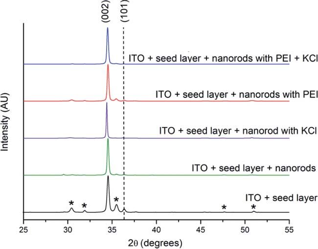
Downing et al.: Solution-processed hybrid photovoltaics: preparation of a standard...

                                 from solution. In addition to PV applications7–11 nanostructured ZnO has been widely used in a
                                 range of applications including light emitting diodes,12–14 thin film transistors,15 and as chemical
                                 sensors.16,17 Nanostructured materials offer significantly larger interfacial areas than bulk films,
                                 however the challenge of preparing nanostructures with tailored and well-defined structures with
                                 high surface-area-to-volume ratios that maximize light harvesting while being compatible with
                                 the short polymer exciton diffusion length has continued to be problematic. Although several
                                 publications detail the formation of h-PV devices based on ZnO nanorods, reported efficiencies
                                 remain modest compared with OPV devices.3,18,19 The formation of metal oxide nanorod scaf-
                                 folds has led to performance improvements compared with planar devices.7,8,18 More recently it
                                 has been shown that blended ZnO:P3HT h-PV devices with efficiencies of 2% can be prepared,6
                                 stimulating further h-PV research.
                                     Clearly a dispersed nanorod array fulfills many of the requirements necessary to improve
                                 device performance. Indeed there have been numerous techniques investigated in an effort to
                                 achieve this goal, including; electrochemical deposition,20,21 template directed growth,22 pulsed
                                 laser deposition,23 and hydrothermal methods.24–27 While solution-based methods tend to favor
                                 the formation of a large number of rods, control of their aspect ratio, spacing, and orientation
                                 has yet to be demonstrated. Vacuum-based methods show potential for morphological control
                                 but are inherently unsuitable for scale-up.
                                     There is a requirement for the preparation of tailored ZnO structures, in which the rod
                                 dimensions, spacing and orientation can be controlled. Such structures would open up a pathway
                                 for further improving h-PV device performance through compatibility with exciton diffusion
                                 length, in addition to providing direct pathways to the electrodes to minimize carrier transport
                                 time and the probability of back electron transfer.19 In this paper a method for the reproducible
                                 preparation of ZnO nanorod arrays using entirely solution-based methods is discussed. In such
                                 arrays the rod aspect ratio can be tuned by varying the growth conditions resulting in uniform
                                 length and vertically aligned structures. More importantly, the rod spacing can also be controlled
                                 which allows structures to be prepared that are ideal for preparing tailored h-PV devices with
                                 controlled separation between donor-acceptor centers.

                                 2 Experimental
                                 ZnO nanorods were created via a two-step solution-based process. First, a seed layer of ZnO was
                                 deposited by spin-coating a 0.75 M solution of zinc acetate dihydrate [Zn(O2 CCH3 ). 2(H2 O),
                                 Sigma-Aldrich] and 2-Aminoethanol [H2 N(CH2 )2 OH, Sigma-Aldrich] in 2-methoxyethanol
                                 [HO(CH2 )2 OCH3 ), Sigma-Aldrich]28 onto indium tin oxide (ITO)-coated glass substrates
                                 (PsiOteC UK Ltd; 12 to 16 /sq). A dense uniform layer was prepared by loading at 500
                                 rpm and increasing the spin speed to 2000 rpm for 30 s. The process was repeated three times
                                 with the substrates briefly heated to 300◦ C between coats. A final 60 min anneal at 450◦ C was
                                 carried out after the layers had been deposited.
                                     In the second step, the as-prepared substrates with ZnO seed layers were suspended up-
                                 side down in an equimolar (25 mM) solution of HMT [NH2 (CH2 )6 NH(CH2 )6 NH2 , Sigma-
                                 Aldrich] and zinc nitrate [(Zn(NO3 )2 , Sigma-Aldrich] at 95◦ C in a similar method described by
                                 Vayssieres.30 The additives 10 mM polyethylenimine [H(NHCH2 CH2 )n NH2, Sigma-Aldrich]
                                 and/or 0.1 M potassium chloride (KCl, Sigma-Aldrich) were added directly to the solution.
                                 Following rod deposition the films were rinsed thoroughly with deionized water and allowed to
                                 dry at 95◦ C.
                                     Scanning electron microscope (SEM) images were obtained using a Leo 1525 field emission
                                 scanning electron microscope. Cross-sectional images of the rod assemblies were obtained to
                                 determine rod length, by scratching or cleaving the substrate. Surface images were used to
                                 measure rod diameter. Data analysis was carried out using ImageJ software.
                                     X-ray diffraction (XRD) patterns were obtained using a Panalytical X’Pert Pro diffractometer
                                 equipped with a monochromated Cu Kα source and an accelerator detector. The voltage and
                                 current were set at 40 kV and 40 mA, respectively.

                                 Journal of Photonics for Energy                                   011117-2                           Vol. 1, 2011

Downloaded From: https://www.spiedigitallibrary.org/journals/Journal-of-Photonics-for-Energy on 29 Oct 2020
Terms of Use: https://www.spiedigitallibrary.org/terms-of-use
Downing et al.: Solution-processed hybrid photovoltaics: preparation of a standard...
Fig. 1 SEM micrographs showing top-surface rod morphology and cleaved cross sections (in-
sets) for ZnO rods grown by hydrothermal method under the conditions, (a) additive free growth,
(b) addition of PEI (10 mM), (c) addition of KCl (100 mM), and (d) combined addition of PEI (10
mM) and KCl (100 mM). Main scale markers 200 nm, inset 500 nm.
3 Results and Discussion
3.1 Seed Layer Growth
Thin ZnO seed layers have been deposited onto ITO substrates by spin-coating a mixed precursor
solution. The method has been adapted to lower the annealing temperature (450◦ C versus 600◦ C).
Differential scanning calorimetry measurements carried out on the zinc acetate precursor show
two distinct regions of mass loss on heating and a sharp crystallization peak at ∼250◦ C on
cooling. The technique results in the formation of polycrystalline thin films, confirmed by SEM
(Fig. 1) and XRD (Fig. 2). Variations in chemical bath conditions and seed layer morphology
have been shown to control rod density, diameter, and morphology.25,27,29
3.2 Nanorod Growth
Rod formation occurs due to preferential growth of ZnO in the 001 direction. This can be
explained by considering the structure of the unit cell. The hexagonal lattice consists of two
networks of tetragonally coordinated Zn and O atoms, this coordination gives rise to polar
asymmetry along the, 001 direction. Nanorod formation is described by Ashford et al.24 for
hydrothermal growth, whereby the high temperature decomposition of hexamethylene triamine
(HMT) results in hydroxyl ion formation. OH− anions produced in the vicinity of the polar ZnO
surfaces are able to react with Zn2+ to produce the insoluble and thermodynamically unstable
Zn(OH)2 species. The spontaneous decomposition of Zn(OH)2 results in the formation of ZnO,
and growth continues at the polar surface resulting in the formation of rod structures. Nucleation
of rod growth occurs on the ZnO seed layer and the structure of the rods is closely related to the
morphology of the seed layer.
Journal of Photonics for Energy 011117-3 Vol. 1, 2011
Downloaded From: https://www.spiedigitallibrary.org/journals/Journal-of-Photonics-for-Energy on 29 Oct 2020
Terms of Use: https://www.spiedigitallibrary.org/terms-of-useDowning et al.: Solution-processed hybrid photovoltaics: preparation of a standard...
Fig. 2 X-ray diffraction patterns obtained from ZnO seed layers and nanorod arrays, curves
labelled from bottom to top; seed layer on ITO (* indicates peaks from ITO substrate), additive-
free nanorod growth, addition of PEI (10 mM), addition of KCl (100 mM), and combined addition
of PEI (10 mM) and KCl (100 mM).
In this work nanorod arrays have been formed from various hydrothermal growth solutions.
The seed layers used were prepared under identical conditions on glass-coated ITO substrates.
First, the method outlined by Vayssieres30 was repeated and resulted in the formation of over-
lapping nanorods with a large variation in the rod length and width [Fig. 1(a)]. The role of a
surfactant [polyethylienmimine (PEI)] was then investigated, it has been reported that reduced
lateral growth of the rods occurs on the addition of PEI.10 The structures typically formed con-
sisted of short nanorods [Fig. 1(b)] that differ from those reported in the literature. We attribute
the variation to differences in the morphology of the seed layers. In the next experiments KCl
was added to the growth solution. It has been well-reported that addition of KCl to an electro-
chemical deposition bath results in the formation of more uniform nanorod structures.31 When
it is added to the hydrothermal growth solution the nanorod arrays prepared show an improved
alignment and the rod length is more uniform with a planar surface termination [Fig. 1(c)]. In
the final series of experiments the addition of both PEI and KCl was investigated. The structures
prepared consist of uniform length nanorods aligned perpendicular to the substrate [Fig. 1(d)].
The combination of the additives gives an increase in rod density that results in very closely
spaced arrays.
For the first time KCl has been shown to play a major role in morphological control of
ZnO nanorods formed by hydrothermal deposition. The addition of KCl is seen to increase rod
nucleation, therefore reducing the spacing between rods, and improve orientation thus ensuring
an open structure for subsequent polymer infiltration. The rods formed when KCl was added
also show well-defined hexagonal facets and are terminated by a planar (002) surface, which
is stabilized during growth by the addition of Cl− .29 PEI is known to hinder lateral growth by
absorbing onto the nonpolar (101) planes.10 The SEM images show a clear variation in the rod
length, width, and density. To assess this, images have been analyzed using ImageJ software to
quantify the average rod length, width, and rod density — the results are summarized in Table 1.
To ensure representative quantities of rods were analyzed, the diameter, length, and density of
250 rods in each sample set were measured. It was not possible to extract meaningful statistics
for the rods formed with the addition of only PEI because of their non-ideal morphology and
broad size distribution [Fig. 1(b)].
Journal of Photonics for Energy 011117-4 Vol. 1, 2011
Downloaded From: https://www.spiedigitallibrary.org/journals/Journal-of-Photonics-for-Energy on 29 Oct 2020
Terms of Use: https://www.spiedigitallibrary.org/terms-of-useDowning et al.: Solution-processed hybrid photovoltaics: preparation of a standard...
Table 1 Rod dimensions and areal density obtained on various nanorod films. Values in brack-
ets display standard deviation.
Average rod diameter Average rod length Areal
(nm) (nm) density/μm2
ITO + seed layer + nanorods (bare) 78 (29) 1283 (387) 45
ITO + seed layer + nanorods with KCl 81 (27) 895 (161) 35
ITO + seed layer + nanorods with KCl 51 (22) 836 (20) 86
and surfactant
3.3 Contact Angle Measurement
The uptake of the rod arrays as electron accepting layers in h-PV devices is reliant on the ability
to form composite structures with semiconducting polymers. Ideally, efficient filling of the
structures would be achieved by filling from solution, hence it is necessary to understand the
wetting behavior of the structures prepared. This was investigated with water as a solvent. Briefly
a 3 μl droplet was added to the surface of various films and the contact angle measured. Large
values of measured contact angle are indicative of poor wetting. The results are summarized in
Table 2.
There is a clear improvement in the wetting behavior with the inclusion of additives into
the growth solution. Importantly, the reported superhydrophobic behavior documented in ZnO
nanorod arrays32,33 is not observed in these structures.
3.4 X-Ray Diffraction
The formation of crystalline ZnO has been confirmed using x-ray diffraction (Fig. 2). The lower
temperature route used in seed layer deposition results in the formation of polycrystalline thin
films with a {002} preferential orientation, consistent with previous reports.25–27 All of the
nanorod structures prepared show the same preferential orientation, which is consistent with the
structures observed by SEM and the proposed growth model.
Analysis of the diffraction data to calculate crystallite size is shown in Table 3, where sizes
for the (002) and (101) diffraction peaks are given. The crystallite sizes calculated from the (002)
diffraction peaks all show an extremely large size (larger than the region for Scherrer analysis),
as is apparent in the peak narrowing observed in the XRD patterns (Fig. 2). The addition of KCl
results in the smallest grain size extracted from the (101) data but the largest out-of-plane grain
size (002), as evidenced by the narrow peak in the XRD pattern. Addition of PEI and the KCl/PEI
mixture led to small increases in the measured (101) crystallite size. The measured (101) sizes
Table 2 Measured contact angle (water) for substrate, seed layer,
and ZnO nanorods.
Substrate Contact angle (deg)
ITO 55
ITO + seed layer 51
ITO + seed layer + nanorods (bare) 15
ITO + seed layer + nanorods with PEI 34
ITO + seed layer + nanorods with KCl 7
ITO + seed layer + nanorods with PEI and KCl 6
Journal of Photonics for Energy 011117-5 Vol. 1, 2011
Downloaded From: https://www.spiedigitallibrary.org/journals/Journal-of-Photonics-for-Energy on 29 Oct 2020
Terms of Use: https://www.spiedigitallibrary.org/terms-of-useDowning et al.: Solution-processed hybrid photovoltaics: preparation of a standard...
Table 3 Calculated crystallite sizes for seed layer and nanorod films prepared
under the conditions described. The addition of KCl is seen to significantly
increase the intensity of the 002 diffraction peaks.
Crystallite size (nm) Crystallite size (nm) 002/101
d(002) d(101) Peak Intensitya
Seed layer 71 56 10
No additives — 105 58
KCl — 46 83
Surfactant — 60 45
KCl and surfactant — 70 141
a Includes contribution from seed-layer.
are similar to those measured for the seed layer, which confirms the role the seed layer has in
controlling nanorod growth. For clarity, normalized (002) spectra are shown, however in the
raw data the addition of KCl increases the intensity of the (002) diffraction peak relative to the
(101) peak indicative of more orientated ZnO being deposited.
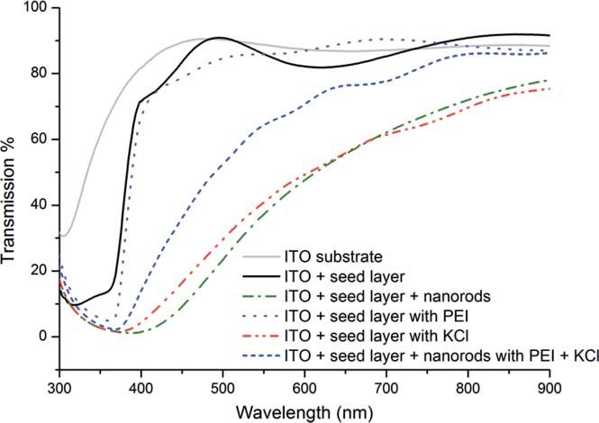
3.5 UV-Visible Spectroscopy
The optical transparency of the films was measured from 300 to 900 nm against an air back-
ground; the results are shown in Fig. 3. The ITO/glass substrate shows a strong absorption at
90% over the 400 to 900 nm
range. The ZnO absorption band (360 nm) is apparent when the seed layer is added to the ITO
and the transparency remains comparable to the bare substrate. The additive-free growth and the
growth with PEI produce films that have significant scattering losses, which we attribute to the
misalignment of the rods. The addition of KCl reduces the scattering and the KCl/PEI mixture
produces a film with similar optical properties to only the seed layer. These films have fewer
scattering losses owing to the morphology of the rods. The aligned structures are also beneficial
for h-PV applications as they have more rods per unit area (increased interfacial area), and with
less overlap between rods there are fewer obstacles to complete polymer infiltration.
Fig. 3 UV-visible data for ITO substrate, seed layer, and nanorod arrays.
Journal of Photonics for Energy 011117-6 Vol. 1, 2011
Downloaded From: https://www.spiedigitallibrary.org/journals/Journal-of-Photonics-for-Energy on 29 Oct 2020
Terms of Use: https://www.spiedigitallibrary.org/terms-of-useDowning et al.: Solution-processed hybrid photovoltaics: preparation of a standard...
4 Conclusions
The development of a nanostructured ZnO template for h-PV applications is described. Hy-
drothermal growth has been identified as an appropriate method for the formation of nanorod
arrays. Unmodified growth results in the formation of ZnO rods with a broad size distribution
and a low density. Furthermore the rods are poorly aligned and overlapping. Orientated rods are
necessary for h-PV applications; more rods per unit area increase interfacial area and matches
closely with the exciton diffusion length in typical organic components. In addition, with less
overlap between rods there are fewer obstacles to complete polymer infiltration, and voids are
seen to be present when filling disordered ZnO structures.11,18
To improve the quality of the rod arrays the influence of additives, PEI and KCl, to the
hydrothermal growth bath was investigated. PEI is reported as an absorbent on the nonpolar
faces of the growing ZnO nanorod while the role of KCl has until now been unreported. The
addition of the surfactant results in the formation of short, tapered, and misaligned rods. The
wetting behavior of the rods is nonideal and the UV-visible spectra show increased scattering.
The addition of KCl significantly improves the uniformity of rod length and width and results
in arrays composed of rods with improved alignment, and well-defined faceted rods are formed.
The improvement in the wetting behavior of these arrays is attributed to the stabilization of the
polar (002) surface at the tip of the rods. The combination of PEI and KCl addition results in
ZnO arrays with the most desirable properties. Rods with a narrow size distribution and a high
number density are prepared; additionally the rods are highly aligned and are terminated by
(002) surfaces that gives rise to the improved wetting behavior. The highly aligned rods reduce
scattering losses, which will be beneficial for h-PV devices, as it will ensure maximum photon
density in the conjugated polymer.
Acknowledgments
Dr Benoit Illy and Joe Franklin for useful discussions. J.D. is supported by EPSRC DTA and in
part by the Energy Futures Lab, Imperial College London. M.A.M. is grateful for the award of
a Royal Academy of Engineering/EPSRC Research Fellowship.
References
1. Q. Zhang, C. S. Dandeneau, X. Zhou, and G. Cao, “ZnO Nanostructures for dye-sensitized
solar cells,” Adv. Mater. 21(41), 4087–4108 (2009).
2. W. J. E. Beek, M. M. Wienk, M. Kemerink, X. N. Yang, and R. A. J. Janssen, “Hybrid
zinc oxide conjugated polymer bulk heterojunction solar cells,” J. Phys. Chem. B. 109(19),
9505–9516 (2005).
3. D. C. Olson, J. Piris, R. T. Collins, S. E. Shaheen, and D. S. Ginley, “Hybrid photovoltaic
devices of polymer and ZnO nanofiber composites,” Thin Solid Films 496(1), 26–29 (2006).
4. M. S. White, D. C. Olson, N. Kopidakis, A. M. Nardes, D. S. Ginley, and J. J. Berry,
“Control of charge separation by electric field manipulation in polymer-oxide hybrid organic
photovoltaic bilayer devices,” Phys. Status Solidi A 207(5), 1257–1265 (2010).
5. M. Helgesen, R. Sondergaard, and F. C. Krebs, “Advanced materials and processes for
polymer solar cell devices,” J. Mater. Chem. 20(1), 36–60 (2010).
6. S. D. Oosterhout, M. M. Wienk, S. S. van Bavel, R. Thiedmann, L. Jan Anton Koster,
J. Gilot, J. Loos, V. Schmidt, and R. A. J. Janssen, “The effect of three-dimensional
morphology on the efficiency of hybrid polymer solar cells,” Nat. Mater. 8(10), 818–824
(2009).
7. D. C. Olson, S. E. Shaheen, R. T. Collins, and D. S. Ginley, “The effect of atmosphere
and ZnO morphology on the performance of hybrid poly(3-hexylthiophene)/ZnO nanofiber
photovoltaic devices,” J. Phys. Chem. C 111, 16670–16678 (2007).
Journal of Photonics for Energy 011117-7 Vol. 1, 2011
Downloaded From: https://www.spiedigitallibrary.org/journals/Journal-of-Photonics-for-Energy on 29 Oct 2020
Terms of Use: https://www.spiedigitallibrary.org/terms-of-useDowning et al.: Solution-processed hybrid photovoltaics: preparation of a standard...
8. D. Olson, Y.-J. Lee, M. S. White, N. Kopidakis, S. E. Shaheen, D. S. Ginley, J. A. Voigt, and
J. W. P. Hsu, “Effect of ZnO Processing on the photovoltage of ZnO/Poly(3-hexylthiophene)
solar cells,” J. Phys. Chem. C 112(26), 9544–9547 (2008).
9. P. Ravirajan, A. M. Peiro, M. K. Nazeeruddin, M. Graetzel, D. D. C. Bradley, J. R. Durrant,
and J. Nelson, “Hybrid polymer/zinc oxide photovoltaic devices with vertically oriented
ZnO nanorods and an amphiphilic molecular interface layer,” J. Phys. Chem. B 110(15),
7635–7639 (2006).
10. M. Law, L. E. Greene, J. Johnson, R. Saykally, and P. D. Yang, “Nanowire dye-sensitized
solar cells,” Nat. Mater. 4(6), 455–459 (2005).
11. Y.-J. Lee, M. T. Lloyd, D. Olson, R. K. Grubbs, P. Lu, R. J. Davis, J. A. Voigt, and J. W. P.
Hsu, “Optimization of ZnO nanorod array morphology for hybrid photovoltaic devices,” J.
Phys. Chem. C 113(35), 15778–15782 (2009).
12. Y. Alivov, E. Kalinina, A. Cherenkov, and D. Look, “Fabrication and characterization of
n-ZnO/p-AlGaN heterojunction light-emitting diodes on 6H-SiC substrates,” Appl. Phys.
Lett. 83(23), 4719–4721 (2003).
13. A. Osinsky, J. Dong, M. Kauser, and B. Hertog, “MgZnO/ AlGaN heterostructure light-
emitting diodes,” Appl. Phys. Lett. 85(19), 4272–4275 (2004).
14. Ü. Özgür, Y. Alivov, C. Liu, A. Teke, M. A. Reshchikov, S. Doǧan, V. Avrutin, S.-J. Cho,
and H. Morkoç, “A comprehensive review of ZnO materials and devices,” J. Appl. Lett.
98(4), 041301 (2005).
15. A. Bashir, P. H. Wöbkenberg, J. Smith, J. M. Ball, G. Adamopoulos, D. D. C. Bradley,
and T. D. Anthopoulos, “High-performance zinc oxide transistors and circuits fabricated
by spray pyrolysis in ambient atmosphere,” Adv. Mater. 21(21), 2226–2231 (2009).
16. O. Lupan, L. Chow, and G. Chai, “A single ZnO tetrapod-based sensor,” Sens. Actuators
B. 141(2), 511–517 (2009).
17. Y.-Z. Lv, C.-R. Li, L. Guo, F. Wang, Y. Xu, and X. Chu, “Triethylamine gas sensor based
on ZnO nanorods prepared by a simple solution route,” Sens. Actuators B 141(1), 85–88
(2009).
18. D. C. Olson, Y.-J. Lee, M. S. White, N. Kopidakis, S. E. Shaheen, D. S. Ginley, J. A.
Voigt, and J. W. P. Hsu, “Effect of polymer processing on the performance of poly(3-
hexylthiophene)/ZnO nanorod photovoltaic devices,” J. Phys. Chem. C 111(44), 16640–
16645 (2007).
19. K. M. Coakley and M. D. McGehee, “Conjugated polymer photovoltaic cells,” Chem.
Mater. 16(23), 4533–4542 (2004).
20. S. Peulon and D. Lincot, “Mechanistic study of cathodic electrodeposition of zinc ox-
ide and zinc hydroxychloride films from oxygenated aquesous zinc chloride solutions,”
J. Electrochem. Soc. 145(3), 864–874 (1998).
21. T. Yoshida, D. Komatsu, N. Shimokawa, and H. Minoura, “Mechanism of cathodic elec-
trodeposition of zinc oxide thin films from aqueous zinc nitrate baths,” Thin Solid Films
451, 166–169 (2004).
22. K. M. Coakley and M. D. McGehee, “Photovoltaic cells made from conjugated polymers
infiltrated into mesoporous titania,” Appl. Phys. Lett. 83(16), 3380–3382 (2003).
23. Y. Sun, G. M. Fuge, and M. N. R. Ashfold, “Growth of aligned ZnO nanorod arrays
by catalyst-free pulsed laser deposition methods,” Chem. Phys. Lett. 396(1–3), 21–26
(2004).
24. M. N. R. Ashfold, R. P. Doherty, N. G. Ndifor-Angwafor, D. J. Riley, and Y. Sun, “The
kinetics of the hydrothermal growth of ZnO nanostructures,” Thin Solid Films 515(24),
8679–8683 (2007).
25. L. E. Greene, M. Law, D. H. Tan, M. Montano, J. Goldberger, G. Somorjai, and P. Yang,
“General route to vertical ZnO nanowire arrays using textured ZnO seeds,” Nano Lett. 5(7),
1231–1236 (2005).
26. J. Song and S. Lim, “Effect of seed layer on the growth of ZnO nanorods,” J. Phys. Chem.
C 111(2), 596–600 (2006).
Journal of Photonics for Energy 011117-8 Vol. 1, 2011
Downloaded From: https://www.spiedigitallibrary.org/journals/Journal-of-Photonics-for-Energy on 29 Oct 2020
Terms of Use: https://www.spiedigitallibrary.org/terms-of-useDowning et al.: Solution-processed hybrid photovoltaics: preparation of a standard...
27. M. Guo, P. Diao, and S. Cai, “Hydrothermal growth of well-aligned ZnO nanorod arrays:
Dependence of morphology and alignment ordering upon preparing conditions,” J. Solid
State Chem. 178(6), 1864–1873 (2005).
28. M. Ohyama, H. Kouzuka, and T. Yoko, “Sol-gel preparation of ZnO films with extremely
preferred orientation along (002) plane from zinc acetate solution,” Thin Solid Films 306(1),
78–85 (1997).
29. D. Boyle, K. Govender, and P. O’Brien, “Novel low temperature solution deposition of
perpendicularly orientated rods of ZnO: Substrate effects and evidence of the importance
of counter-ions in the control of crystallite growth,” Chem. Commun. 2002, 80–81 (2002).
30. L. Vayssieres, “Growth of arrayed nanorods and nanowires of ZnO from aqueous solutions,”
Adv. Mater. 15(5), 464–466 (2003).
31. B. N. Illy, B. Ingham, and M. P. Ryan, “The effect of the supersaturation on the growth
of zinc oxide nanostructured films by electrochemical deposition,” Crys. Growth Des. 10,
1189–1193 (2010).
32. C.-T. Hsieh, S.-Y. Yang, and J.-Y. Lin, “Electrochemical deposition and superhydrophobic
behavior of ZnO nanorod arrays,” Thin Solid Films 518(17), 4884–4889 (2010).
33. X. Zhu, Z. Zhang, X. Men, J. Yang, and X. Xu, “Fabrication of an intelligent superhy-
drophobic surface based on ZnO nanorod arrays with switchable adhesion property,” Appl.
Surf. Sci. 256(24), 7619–7622 (2010).
Biographies and photographs of the authors not available.
Journal of Photonics for Energy 011117-9 Vol. 1, 2011
Downloaded From: https://www.spiedigitallibrary.org/journals/Journal-of-Photonics-for-Energy on 29 Oct 2020
Terms of Use: https://www.spiedigitallibrary.org/terms-of-useYou can also read