Synthesis for Manufacturability: a Sanity Check

Page created by Pedro Pierce
 
CONTINUE READING
Synthesis for Manufacturability: a Sanity Check
∗
                           Synthesis for Manufacturability: a Sanity Check
                     Alessandra Nardi                Alberto L. Sangiovanni-Vincentelli
                  EECS Department, University of California at Berkeley, Berkeley, CA 94720
                                                {nardi,alberto}@eecs.berkeley.edu

                             Abstract                                      on circuit performance caused by process variations; func-
                                                                           tional (or catastrophic) yield loss refers to physical and
    As we move towards nanometer technology, manufac-                      structural defects that cause the circuit to fail completely.
turing problems become overwhelmingly difficult to solve.                     In deep-submicron new technology nodes, yield im-
Presently, optimization for manufacturability is performed                 provement is as much a design problem as it is a manu-
at a post-synthesis stage and has been shown capable of re-                facturing problem. Presently, manufacturing optimization
ducing manufacturing cost up to 10%. As in other cases,                    is performed at a post-synthesis stage: first synthesis tar-
raising the abstraction layer where optimization is applied                gets area and timing [2, 1], then the design is optimized
is expected to yield substantial gains. This paper focuses on              for yield at the layout level. This optimization might in-
a new approach to design for manufacturability: logic syn-                 volve adding redundancy to contacts and vias, modifying
thesis for manufacturability. This methodology consists of                 the spacing between existing interconnections, and replac-
replacing the traditional area-driven technology mapping                   ing cell instances with higher yielding variants, placed in
with a new manufacturability-driven one. We leverage ex-                   the same position as their original ones. The reason place-
isting logic synthesis tools to test our method. The results               ment is not perturbed is to avoid costly repetition of the
obtained by using STMicroelectronics 0.13µm library con-                   optimization aimed at maximizing speed and minimizing
firm that this approach is a promising solution for design-                area. Traditional post-synthesis yield optimization has been
ing circuits with lower manufacturing cost, while retaining                shown capable of reducing manufacturing cost by up to
performance. Finally, we show that our synthesis for man-                  10% [5, 10].
ufacturability can achieve even larger cost reduction when
yield–optimized cells are added to the library, thus enabling                 Extensive work has been devoted to understanding cir-
a wider area-yield tradeoff exploration.                                   cuit sensitivity to these failure mechanisms and to reducing
                                                                           catastrophic yield loss [7, 6, 3, 4, 8, 9]. Heineken et al. [5]
                                                                           present an attempt to make this optimization less of an art-
                                                                           work process. In their approach, yield-optimized cells are
1. Introduction                                                            generated and then substituted in the synthesized design.
                                                                           However, their algorithm is limited to an in-place substitu-
   Traditionally, design methodologies (and the supporting                 tion to preserve the footprint of the original design.
tools and flows) for Integrated Circuits target nominal de-
signs. However, defects and variations present in the IC                      Following the general rule that the higher the level of ab-
manufacturing process may cause the circuit to behave dif-                 straction the larger the horizon for optimization, we propose
ferently from the nominal design in a substantial way. In                  a synthesis for manufacturability approach, in which manu-
particular, in deep submicron technologies, manufacturing                  facturability is part of the cost function that drives synthesis.
process variations and defects may turn a successful design                The necessity of including manufacturability (and testabil-
into a failure. Design For Manufacturability (DFM) is of                   ity) in the synthesis cost function was advocated in Shaik et
strategic importance to decrease VLSI IC’s manufacturing                   al. [11], but, to the best of our knowledge, we are the first
cost. DFM methods allow to estimate yield and robustness                   to address this issue.
during the design phase, prior to manufacturing.                              The paper, focused on a synthesis-based methodology
   Yield is defined as the percentage of manufactured prod-                to improve functional yield loss, is organized as follows:
ucts that meet all performance and functionality specifi-                  Section 2 briefly introduces the new approach we propose,
cations. Parametric yield loss usually refers to the effects               Section 3 provides some background on the catastrophic
                                                                           yield modeling problem, Section 4 reports the heuristics we
∗   This work was partially supported by the Microelectronics Innovation   implemented and the related experimental results are de-
    and Computer Research Opportunities (MICRO) program.                   scribed in Section 5.
2. Synthesis For Manufacturability                                 In our approach, performance is still the first target dur-
                                                                ing optimization. In fact, as the standard flow tries to op-
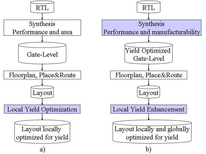
    The current “yield-aware” design flow (Figure 1.a) [2, 1]   timize area on non-critical paths, the synthesis for manu-
is an optimization process with two main objectives: max-       facturability approach tries to optimize manufacturability
imum speed and minimum area. The design is then pro-            (a combination of area and layout sensitivity to defects) on
cessed for yield enhancement at the layout level. The new       non-critical paths as well.
design paradigm we propose is illustrated in Figure 1.b:
manufacturability is introduced to replace area in the cost
function. The advantages of this approach are presented in
                                                                3. Background
Section 5.1. Clearly this new approach is transparent to de-        In this Section we briefly review the catastrophic yield
signers who will only have to choose whether to target min-     modeling problem definition: the focus is not on a rigorous
imum area or minimum manufacturing cost.                        statistical modeling for yield prediction, rather we intend to
                                                                provide an intuitive view that will lead us to understand the
                                                                new cost function we use propose to use during synthesis
                                                                and the related results.
                                                                    Various different types of defects are introduced during
                                                                the manufacturing process. These defects may, for example,
                                                                result into open or short circuits. However, not all defects
                                                                will necessarily cause a circuit failure: functional yield loss
                                                                depends, in fact, on the wafer defectivity and on the design
                                                                attributes.
                                                                    The figure that is commonly used to quantify layout sen-
                                                                sitivity to defects is the critical area. Critical area Aci (x) for
                                                                defects of type i and diameter x is defined as the size of
                                                                the area in which the center of defect of type i and diam-
                                                                eter x must fall in order to cause a circuit failure. We in-
                                                                dicate as Aci the critical area for defects of type i averaged
                                                                over all defect diameters x:
                                                                                           Z
                                                                                    Ai = Aci (x)fd (x)dx
                                                                                      c
                                                                                                                                (1)
   Figure 1. a) Standard flow and b) Synthesis
   for manufacturability approach
                                                                where fd (x) is the defect probability density function.
                                                                   Finally, let di denote the average number of defects of
                                                                type i per unit area, then the average number of faults on
                                                                the circuit is:
    A further development to the new design for manufac-                                    X
turability paradigm is to incorporate yield during standard                            λ=      Aci · di                  (2)
                                                                                               i
cell design: in addition to variants for high speed and low
power, variants for high yield could also be included. In          where the sum is taken over all possible defects types on
Section 5.2, we report a preliminary analysis on how our        the circuit [8].
new technology mapping heuristics could exploit these li-          It can be shown that, in general, for a given design com-
braries with yield-optimized variants to reduce manufactur-     ponent b, yield may be expressed as:
ing cost.
                                                                                           Yb = e−λb                           (3)
    Comparing Figures 1.a and 1.b, one can observe that
our approach focuses on choosing the best gate mapping          where λb is the failure rate of component b.
prior to physical synthesis as opposed to manually or semi-         Assuming that gates are statistically independent com-
automatically perform an in-place optimization limited by       ponents and defects are uniformely distributed (Poisson
the design placement. This methodology is a global op-          model), yield for a circuit with N gates, can be expressed
timization and can be effectively complemented by tradi-        as:
tional local optimization once the design has been layed                                         Y
                                                                                                 N

out. Clearly, additional improvements can be achieved dur-                          Ycircuit =     YG,k                 (4)
ing the routing phase (e.g. [6]). Other circuit techniques,                                        k=1

such as adding redundancy to render the circuit robust to       where N is the number of circuit gates and YG,k is the yield
failure [8], are also out of the scope of this paper.           of a single gate averaged with respect to different defect
types and size. Referring to Equation (3), the circuit yield       not so straightforward for effective yield. In fact, assum-
becomes:                                                           ing wafer area Awaf er is given, for synthesis for manufac-
                         PN                                        turability the optimization problem becomes:
          Ycircuit = e− k=1 λG,k = e−λcircuit            (5)                                         QN
                                                                                         Ycircuit      k=1 YG,k
   It has been shown that this model is pessimistic for yield                     max             = PN                      (7)
                                                                                         Acircuit      k=1 AG,k
values prediction due to the fact that defects are not uni-
formely distributed, but rather tend to cluster.                   or equivalently:
   There is a vast literature (e.g. [8, 12]) on how to de-
                                                                                                     PN
rive a model to accurately predict yield with clustered de-                               Acircuit        AG,k
fect distributions. Nevertheless, our research is aimed at an-                    min              = Qk=1
                                                                                                      N
                                                                                                                                 (8)
                                                                                          Ycircuit    k=1 YG,k
alyzing how synthesis for manufacturability can lower man-
ufacturing cost rather than doing an exact yield prediction.           where Acircuit and Ycircuit are area and yield of the cir-
Therefore, we will use the simple Poisson model (4) to-            cuit respectively, while AG,k and YG,k are area and yield
gether with the failure rate description (5) to focus on yield     of the single gates composing the circuit. The cost function
increase/decrease rather than its exact value.                     for the optimization problem described in Equation (8) is
   Finally, it is important to make a distinction between the      not simply additive and therefore we need to devise a good
effective yield of a circuit Yef f,circuit , defined as the num-   heuristic to approximate it.
ber of “good” circuits per wafer and the yield of a circuit            Here we report some observations on different heuristics
Ycircuit defining the percentage of “good” circuits. They are      and in Section 5, we provide the corresponding experimen-
related through the equation:                                      tal results.
                                                                       Heuristic 1: Yield Only. An intuitive approach would be
              Yef f,circuit = Ncircuit · Ycircuit           (6)    to try to improve circuit yield by decreasing layout sensitiv-
where Ncircuit is the number of circuits in the wafer.             ity to defects as described by Equations (2) and (3). There-
    To lower the manufacturing cost of a circuit we need to        fore, recalling Equations (5) and (4), the optimization prob-
improve its effective yield, that is to achieve a better trade-    lem becomes:
off between yield and the actual number of circuits that can                              Y
                                                                                          N                PN
                                                                                                                    λG,k
fit in a given wafer area.                                                       max           YG,k = e−      k=1                (9)
    Recalling Equations (2) and (3) we can observe that yield                            k=1
loss is due to the combination of two effects: the presence
                                                                   or its equivalent additive form:
of a defect and the sensitivity of the component to the de-
fect. Assuming we cannot influence the defect distribution,                                      Y
                                                                                                 N                 X
                                                                                                                   N
we are left to decrease the circuit sensitivity and perform a           min |ln(Y )| = |ln(            YG,k )| =         λG,k   (10)
trade-off with circuit area: this is the goal of synthesis for                                   k=1               k=1
manufacturability.
                                                                   In practice, this would mean to minimize the critical area
                                                                   (or equivalently the failure rate), disregarding the actual cir-
4. Technology Mapping Heuristics for Manu-                         cuit area.
   facturability                                                      Heuristic 2: Weighted Yield. While in the previous
    This Section presents different heuristics analyzed to         heuristic area is not taken into account, it can be easily in-
implement our new synthesis for manufacturability ap-              troduced as a weigthing factor in equation (10) and turn the
proach depicted in Figure 1.b. The goal is to have an              optimization problem into:
indication of the usefulness of this approach: this preli-
                                                                                X
                                                                                N                          X
                                                                                                           N
mary exploration phase is based on the modification of                  min           |AG,k ln(YG,k )| =         AG,k λG,k      (11)
the well-estabilished technology mapping algorithm avail-                       k=1                        k=1
able in commercial tools such as Synopsys Design Com-
piler [1]. Given the fact that performance is the pri-                Heuristic 3: Manufacturability Function Approxima-
mary objective, some flexibility is left on area along the         tion. A more sophisticated approach is to approximate the
non-critical paths: the key idea is to exploit this flexibil-      original cost function as closely as possible with an addi-
ity to obtain a higher effective yield by manipulating yield       tive function. We adopt the following approximation for the
and area instead of simply area.                                   optimization problem:
    In state-of-the-art tools, technology mapping is per-                            PN              X
                                                                                                     N
formed using a dynamic programming algorithm which re-                    Acircuit        AG,k         AG,k
                                                                    min            = Qk=1
                                                                                      N
                                                                                               ≈ min    p   (12)
lies on the fact that area is an additive funtion. Things are             Ycircuit        Y
                                                                                      k=1 G,k
                                                                                                       YG,k
                                                                                                                      k=1
where p is a parameter that can be chosen to tune up the
heuristic.                                                                                                           1.2

                                                                       Failure rate ratio wrt area optimization
   An intuitive choice is p = 1, but we will show that
                                                                                                                      1
p = N is actually a better value. The reason for choos-
                                                    0
ing p = N becomes evident if we approximate all YG,k   s                                                             0.8                                          A
                                                                                                                                                                  Y
                                1
with a common average value Ya :                                                                                                                                  ALNY
                                                                                                                     0.6                                          AY

X
N               PN                PN                PN                                                                                                            AYN
      AG,k         k=1 AG,k              AG,k               AG,k                                                                                                  AYN100

       N
           ≈                  = Qk=1
                                  N
                                                ≈ Qk=1
                                                   N
                                                                                                                     0.4                                          AYN1000
      YG,k          YaN               k=1 Ya           k=1 YG,k
k=1                                                                                                                  0.2

   We explored different values of p and experimental re-
                                                                                                                      0
sults are reported in Section 5.                                                                                           s38594    clma   C7552   apex2   seq

                                                                                                                                              a)
5. Experimental Results                                                                                               3

   As we mentioned in Section 2, the synthesis for man-

                                                                       Area ratio wrt area optimization
                                                                                                                     2.5
ufacturability can be envisioned in two steps: the first is
to change the synthesis cost function to include yield and                                                            2                                           A
                                                                                                                                                                  Y
the second is to enrich the standard cell library with yield-                                                                                                     ALNY
                                                                                                                     1.5                                          AY
optimized gates.                                                                                                                                                  AYN
   In Subsection 5.1 we show that significant improvement                                                             1
                                                                                                                                                                  AYN100
                                                                                                                                                                  AYN1000
can already be achieved at no-cost for designer and library
developers, i.e. by only changing the synthesis cost func-                                                           0.5

tion. Further reduction of manufactuting cost can be ob-
                                                                                                                      0
tained when yield-optimized gates are added to the library                                                                 s38594    clma   C7552   apex2   seq
(similarly to having speed-optimized or low-power ver-
                                                                                                                                              b)
sions): preliminary results are reported in Subsection 5.2.
                                                                       Effective yield ratio wrt area optimization

                                                                                                                     1.2

5.1. Technology mapping for manufacturability                                                                         1

   We evaluated the different heuristics proposed in Sec-                                                            0.8                                          A
                                                                                                                                                                  Y
tion 4 on testcases from the IWLS93 benchmark suite                                                                                                               ALNY
mapped on STMicroelectronics 0.13µm standard cell li-                                                                0.6                                          AY
                                                                                                                                                                  AYN
brary. Since yield data for the standard cell library were not                                                                                                    AYN100
                                                                                                                     0.4                                          AYN1000
available to us, we assigned a yield value to each gate by as-
suming the failure rate F R to be a random variable with a                                                           0.2
uniform distribution in (300ppb, 500ppb).
   Results from heuristics evaluation are reported in Fig-                                                            0
                                                                                                                           s38594    clma   C7552   apex2   seq
ure 2: the bottom table explains the correspondence be-
tween the symbols in the legend and the function used as                                                                                      c)
heuristic.
   Figure 2 reports the failure rate (a), the area (b) and the                                         Symbol                       A Y        ALNY         AY
effective yield (c) normalized to values obtained from the                                             Heuristic                    A |ln(Y )| |A · ln(Y )| A/Y
standard synthesis optimization based solely on area (indi-                                            Symbol                       AYN     AYN100      AYN1000
cated as A).                                                                                           Heuristic                    A/Y N   A/Y 100N A/Y 1000N
   These data confirm the observations we reported in Sec-
tion 4: the best results for failure rate reduction are ob-           Figure 2. Comparison of different heuris-
tained by performing optimization solely based on yield (Y )          tics for synthesis for manufacturability on
and secondly by using yield weighted by area (ALN Y ).                IWLS93 benchmark. Data are normalized with
Nevertheless, as expected, these heuristics perform poorly            respect to results obtained with the standard
for area: overall, the effective yield is worsened by these           synthesis flow.

1   This approximation seems reasonable given the typical values of
    YG,k = e−F RG,k ' 1 − F RG,k with F RG,k
Function       s38584     clma     C7552      apex2     seq                                                 1.1

                                                                       Projected ratio of effective yield
 A              1          1        1          1         1                                                  1.08
 |ln(Y )|       0.61       0.37     0.36       0.46      0.46                                               1.06
 |Aln(Y )|      0.90       0.95     0.93       0.90      0.91                                               1.04
 A/Y            1          1        1          1         1                                                  1.02
 A/Y N          1.0001     0.99     1.001      1.0002    1.006                                                1
 A/Y 100N       0.99       0.99     1.002      0.99      1.005
                                                                                                            0.98
 A/Y 1000N      0.90       0.94     1.0009     0.98      0.99
                                                                                                            0.96

                                                                                                            0.94
   Table 1. Effective yield ratio with respect to

                                                                                                                 94

                                                                                                                                               2

                                                                                                                                                       17
                                                                                                                         a

                                                                                                                               ip

                                                                                                                                      88

                                                                                                                                              52

                                                                                                                                                        q

                                                                                                                                                              la

                                                                                                                                                                        3
   standard synthesis optimization on IWLS93

                                                                                                                                             ex

                                                                                                                                                      se

                                                                                                                                                                      ex
                                                                                                                         m

                                                                                                                             ds

                                                                                                                                                            sp
                                                                                                               85

                                                                                                                                                     84
                                                                                                                                    62

                                                                                                                                            75
                                                                                                                      cl

                                                                                                                                           ap

                                                                                                                                                                   is
                                                                                                             s3

                                                                                                                                                   s3
                                                                                                                                    C

                                                                                                                                           C

                                                                                                                                                               m
   circuits.
                                                                      Figure 3. Projection of results of synthesis
                                                                      for manufacturability on repetition of seed
heuristics (Figure 2.c and Table 1). The last four colums             circuits to constitute a 1cm2 area.
of the chart correspond to different values of p using the
heuristic in Equation (12). Table 1 confirms the results pre-
dicted in the previous Section: assuming yield follows a               To show how this can lead to a higher effective yield, we
Poisson model, p = N leads to best results for effective           developed a virtual variant for each of the original standard
yield. As an additional remark, the error due to the approx-       cells from the STMicroelectronics 0.13µm library. Yield
imation described in Equation (12) is less than 0.1% with          improvement has been modeled by using a random vari-
p = N , while it can reach values up to 20% by using               able F R f actor with a uniform distribution in (1, 10) to
p = 100N . Furthermore, results from a number of other             divide the original cell failure rate F R. In other words, for
testcases from the IWLS93 benchmark, confirm the valid-            each cell, the new variant’s failure rate will be decreased
ity of choice p = N : therefore, we will use this heuris-          randomly from a value in (300ppb, 500ppb) to a value in
tic to drive our technology mapping algorithm in the fol-          (30ppb, 500ppb). According to past literature [5], manu-
lowing experiments. Notice that, AY gives the same re-             facturability can be improved with small or no penalty in
sults as the standard optimization for area. This is due to        area (or even area reduction). We assumed that 80% of cell
the fact that for a single gate, yield Y = e−F R is “almost”       variants will suffer from area increase, while the remaining
1. These high yield values for the single cell are the rea-        20% will benefit from yield increase with no area penalty.
son why we explored giving larger importance to yield, by          Clearly this is a conservative assumption and better results
using p = 100N and p = 1000N .                                     can be achieved with more advantageous trade-offs. The
    It is worth noticing that the circuits reported above are      cells to suffer from area penalty are chosen randomly and
quite small and this explains the relatively small improve-        area is increased by a discrete quantity (technology pitch
ment in effective yield. To evaluate the impact that synthe-       multiplied by the cell height).
sis for manufacturability can have on larger circuits, we cre-         Circuits from the IWLS93 benchmark were synthesized
ated a 1cm2 circuit constituted of a repetition of a single cir-   on the enhanced library containing both the original cells
cuit (called seed).                                                and the high-yield variants. Both the standard flow (opti-
    We estimated the projected effective yield value on 1cm2       mization for area) and synthesis for manufacturability have
circuits by using as seed for replication some IWLS93 cir-         been used (implementing heuristic AY N ).
cuits. Results are reported in Figure 3: effective yield im-           As done in the previous Subsection, to obtain a projec-
provement can be as large as 9%. As a final observation, it        tion of effective yield improvement on large circuits we
is worth recalling that this substantial improvement is ob-        replicated the IWLS93 circuits to form 10mm2 (Figure 4.a)
tained at absolutely no cost for designers and library devel-      and 1cm2 (Figure 4.b) areas. Data show that a substan-
opers, assuming yield information are available.                   tial effective yield improvement can be obtained by using
                                                                   the synthesis for manufacturability flow on the extended li-
                                                                   braries.
5.2. Further improvement: yield-optimized gates
                                                                       Remarks All the experiments are based on the Poisson
   As we already mentioned, results obtained in Sec-               yield model. As discussed in Section 3, this model typically
tion 5.1 can be further improved by using libraries with           produces a lower bound on the effective yield.
yield-optimized variants in addition to the cells opti-                The goal of this paper is to highlight the trend of man-
mized for speed and/or area.                                       ufacturability improvement that can be obtained using the
have been presented to implement this methodology us-
                                          1.16                                                                           ing Synopsys Design Compiler. The new approach is com-
     Projected ratio of effective yield

                                          1.14                                                                           pletely transparent to designers and library developers and
                                          1.12                                                                           results on the IWLS93 benchmark show it may lead to sig-
                                           1.1                                                                           nificant effective yield improvement. Further cost reduction
                                          1.08                                                                           is observed by extending the standard cell library to in-
                                          1.06
                                                                                                                         clude yield-optimized variants and using the new technol-
                                          1.04
                                                                                                                         ogy mapping heuristics.
                                          1.02
                                            1
                                          0.98
                                                                                            2
                                                                                                                         Acknowledgments
                                                84

                                                            a

                                                                                                     17

                                                                                                                     3
                                                                  ip

                                                                          88

                                                                                  15

                                                                                                      q

                                                                                                            la
                                                                                                                            The authors would like to thank Claudio Pinello for the
                                                                                         ex

                                                                                                                   ex
                                                         m

                                                                                                   se
                                                                ds

                                                                                                          sp
                                             85

                                                                        62

                                                                                53

                                                                                                  84
                                                      cl

                                                                                       ap

                                                                                                                  is
                                           s3

                                                                       C

                                                                               C

                                                                                                s3

                                                                                                                 m
                                                                                                                         many useful suggestions and Enrico Malavasi, Michael Or-
                                                                                  a)                                     shansky and Farhana Sheikh for the discussions during the
                                                                                                                         prelimary phase of this research.
                                          4.5
     Projected ratio of effective yield

                                           4
                                          3.5                                                                            References
                                           3
                                          2.5                                                                             [1] Design Compiler User’s Manual. Synopsys Inc., 1998.
                                           2                                                                              [2] Logic Synthesis and Verification. Kluwer Academic Publish-
                                          1.5                                                                                 ers, 2002.
                                           1                                                                              [3] V. K. R. Chiluvuri and I. Koren. Layout-synthesis techniques
                                          0.5                                                                                 for yield enhancement. IEEE Transactions on Semiconduc-
                                           0                                                                                  tor Manufacturing, 8(2):178–187, May 1995.
                                                                                                                          [4] V. K. R. Chiluvuri and I. Koren. Yield enhancement vs.
                                                                                            2
                                               84

                                                        a

                                                                                                     17

                                                                                                                    3
                                                                  ip

                                                                          88

                                                                                  15

                                                                                                      q

                                                                                                            la
                                                                                         ex

                                                                                                                  ex
                                                        m

                                                                                                   se
                                                                ds

                                                                                                          sp
                                            85

                                                                        62

                                                                                53

                                                                                                  84
                                                     cl

                                                                                       ap

                                                                                                                  is

                                                                                                                              performance improvement in vlsi circuits. In International
                                          s3

                                                                       C

                                                                               C

                                                                                                s3

                                                                                                                 m

                                                                                  b)                                          Symposium on Semiconductor Manufacturing, pages 28–31,
                                                                                                                              Sept. 1995.
   Figure 4. Projection of the ratio of effec-                                                                            [5] H. T. Heineken, J. Khare, and M. d’Abreu. Manufacturability
   tive yield using IWLS93 benchmark to obtain                                                                                analysis of standard cell libraries. In Proceedings of the IEEE
   10mm2 a) and 1cm2 b) circuits. Data are nor-                                                                               1998 Custom Integrated Circuits Conference, pages 321–4,
   malized with respect to results obtained by                                                                                May 1998.
   using the standard synthesis flow.                                                                                     [6] H. T. Heineken and W. Maly. Interconnect yield model
                                                                                                                              for manufacturability prediction in synthesis of standard cell
                                                                                                                              based designs. In Proceedings of International Conference
                                                                                                                              on Computer-Aided Design, pages 368–373, Nov. 1996.
new heuristics for the technology mapping algorithm. Al-                                                                  [7] H. T. Heineken and W. Maly.                      Performance-
though we do not compute exact yield values, we expect                                                                        manufacturability tradeoffs in IC design. In Proceed-
that an increase in yield lower bounds will also lead to a de-                                                                ings of Design, Automation and Test in Europe, pages
crease in the defect sensitivity and to an increase of yield ex-                                                              563–567, Feb. 1998.
act values. Hence, a more accurate yield model is expected                                                                [8] I. Koren and Z. Koren. Defect tolerance in VLSI circuits:
to give a similar trend.                                                                                                      techniques and yield analysis. Proceedings of the IEEE,
   Finally, when using different yield and process models,                                                                    86(9):1819–1838, Sept. 1998.
we can either use a different heuristic to better match data,                                                             [9] W. Maly, H. T. Heineken, J. Khare, and P. K. Nag. Design for
or we can simply tune the value of p in Equation (12). In                                                                     manufacturability in submicron domain. In Proceedings of
                                                                                                                              International Conference on Computer-Aided Design, pages
fact, we have shown that increasing p increased the weight
                                                                                                                              690–697, Nov. 1996.
of yield in the manufacturability cost function.                                                                         [10] C. Ouyang, H. T. Heineken, J. Khare, S. Shaikh, and
                                                                                                                              M. d’Abreu. Maximizing wafer productivity through layout
6. Conclusions                                                                                                                optimizations. In Proceedings of 13th International Confer-
                                                                                                                              ence on VLSI Design, pages 192–197, Jan. 2000.
   Methodologies to increase manufacturability are of ut-                                                                [11] S. A. Shaikh, J. Khare, and H. T. Heineken. Manufacturabil-
most importance to lower manufacturing costs for deep sub-                                                                    ity and testability oriented synthesis. In Proceedings of 13th
micron technologies. Post-layout optimization has a lim-                                                                      International Conference on VLSI Design, pages 185–191,
ited impact, hence we propose a new synthesis for manu-                                                                       Jan. 2000.
facturability approach to target effective yield early in the                                                            [12] D. M. H. Walker. Yield simulation for integrated circuits.
design stage. Different heuristics for technology mapping                                                                     Kluwer Academic Publishers, 1987.
You can also read