TIN FILMS DEPOSITED ON URANIUM BY HIGH POWER PULSED MAGNETRON SPUTTERING UNDER LOW TEMPERATURE - MDPI
←
→
Page content transcription
If your browser does not render page correctly, please read the page content below
materials
Article
TiN Films Deposited on Uranium by High Power
Pulsed Magnetron Sputtering under
Low Temperature
Jingjing Ding, Xixi Yin, Liping Fang          ID
                                                   , Xiandong Meng and Anyi Yin *
 Institute of Material, China Academy of Engineering Physics, Mianyang 621900, China;
 dingjingjing21@126.com (J.D.); yinxixi@caep.com (X.Y.); fanglp26@163.com (L.F.);
 mengxiandong@caep.cn (X.M.)
 * Correspondence: anyiyin@126.com; Tel.: +86-0816-3626746

 Received: 10 July 2018; Accepted: 6 August 2018; Published: 10 August 2018

 Abstract: Depleted uranium (DU) is oxidized readily due to its chemical activities, which limits
 its applications in nuclear industry. TiN film has been applied widely due to its good mechanical
 properties and its excellent corrosion resistance. In this work, TiN protection films were deposited on
 DU by direct current magnetron sputtering (DCMS) and high power pulsed magnetron sputtering
 (HPPMS), respectively. The surface morphology and microstructures were investigated by atomic
 force microscope (AFM), scanning electron microscopy (SEM), and grazing incidence X-ray diffraction
 (GIXRD). The hardness and Young’s modulus were determined by nano-Indenter. The wear behavior
 and adhesion was analyzed by pin-on-disc tests and scratch adhesion tests and the corrosion
 resistance was evaluated by electrochemical measurements. The results show that the TiN films
 that were deposited by HPPMS outperformed TiN film deposited by DCMS, with improvements on
 surface roughness, mechanical properties, wear behavior, adhesion strength, and corrosion resistance,
 thanks to its much denser columnar grain growth structure and preferred orientation of (111) plane
 with the lowest strain energy. Besides, the process of Ti interlayer deposition by HPPMS can enhance
 the film properties to an extent as compared to DCMS, which is attributed to the enhanced ion
 bombardment during the HPPMS.

 Keywords: DU; TiN film; HPPMS

1. Introduction
     Uranium is widely used in civilian and military applications due to its unique nuclear
properties. However, it is chemically active and susceptible to corrosion, especially in salty, humid,
and high-temperature environments [1,2]. Surface modification and film techniques have been applied
to improve the corrosion resistance of U, including Ni [3], Al [4], Ti-based [5], Cr-based [6] films,
and Mo+ , C+ , N+ [7,8] ion-implantation. These films can increase corrosion resistance to a certain
extent. However, it is hard to get a pure surface without oxidation for films deposited on depleted
uranium due to its high chemical activity. Inevitably, an undesirable interface adhesion and loose
structure is induced. Consequently, the spallation failure of films and corrosion of the substrate easily
occur. Thus, there exists an urgent demand for preparing a film with good performance to improve
the serve life of depleted uranium (DU).
     TiN films have been commonly used for protective purposes on different kinds of substrate
materials due to its chemical stability and excellent mechanical properties [9–13]. However, the
deposition temperature of TiN is above 300 ◦ C in most reported literature [14], which is too high for
DU for the following two facts: (1) the thick and loose uranium oxide layer that is formed at this

Materials 2018, 11, 1400; doi:10.3390/ma11081400                               www.mdpi.com/journal/materials
Materials 2018, 11, 1400                                                                           2 of 13

temperature would decrease the interfacial adhesion strength between film and substrate intensively;
(2) when uranium components are subjected to such high temperatures, they may deform and lose
their mechanical properties. Until now, the film deposition under low temperature is still one of the
most critical engineering and scientific problems that challenge the film application on uranium.
     Efforts have been attempted to deposit TiN film on DU under low temperature by various
methods including the conventional direct current magnetron sputtering (DCMS) and arc ion
plating (AIP) techniques [5]. However, existing techniques encounter such difficulties as: the films
deposited by DCMS at low temperature often exhibit a loose structure due to the low ionization rate
of less than 1% [15]; AIP has high ionization rate, however, the macroscopic droplets produced
in the film deposition process would result in some void defects and decrease the corrosion
resistance consequently.
     High power pulsed magnetron sputtering (HPPMS) is a novel technique in which the power
provides the target with pulses of high power densities of a few kW cm−2 . This technology enriched
in metal ion plasma, could deposit dense structures and offer virtually defect free films at a relatively
low temperature [16,17].
     In this work, HPPMS technique was utilized to deposit dense TiN films on uranium for the first
time. TiN films were deposited on DU by DCMS and HPPMS. The surface roughness, morphology,
nano-hardness, adhesion strength, and electrochemical properties of these films were characterized in
order to study the differences between conventional DCMS and HPPMS.

2. Materials and Methods

2.1. Sample Preparation
     The Ti/TiN films were deposited on DU substrate and silicon (100) wafers, the later ones were
prepared for phase and morphology analysis. The DU samples with a size of Φ15 mm × 3 mm were
grinded using SiC water papers from 500# to 1000# progressively, mechanically polished to minor,
and ultrasonically cleaned in acetone and ethanol, respectively, and then put into a vacuum chamber
immediately when the substrates dried.
     The base pressure was lower than 5 × 10⁻⁴ Pa and the chamber temperature was fixed to
180 ◦ C. Prior to deposition, the DU samples were sputtered by Ar+ ions (2.0 Pa, applied bias voltage
−800 V) for 30 min to clean the surface contaminations and partially remove the native oxide layer.
After pre-sputtering, the Ti interlayer of approximately 100~300 nm thick was pre-deposited on the
DU substrates to reduce the stress at the substrate interface and to enhance the adhesion between
the film and the substrate. During deposition, the TiN films were deposited on the substrate with
thickness of 4~5 µm.
     Three deposition modes were designed to compare the structure and properties of the films
deposited by HPPMS and DCMS, in order to investigate how the high power pulse introduced
into magnetron sputtering process influences performance of the TiN films. Table 1 summarizes
the deposition parameters for TiN film fabricated by DCMS, HP + DC, and HPPMS modes. In the
DCMS mode, both Ti interlayer and TiN film were deposited by DCMS. In the HP + DC mode, the Ti
interlayer was prepared by HPPMS, and then TiN layer by DCMS. However, in the HPPMS mode, both
Ti interlayer layer and TiN film were deposited by HPPMS. The cathode was operated in a vacuum
chamber equipped with a HPPMS power supply by employing the following parameters: frequency of
150 Hz, pulse width of 200 µs, and average power of 2.2 kW. The applied bias voltage of the substrate
was −100 V. The deposition gas pressure was 0.3 Pa.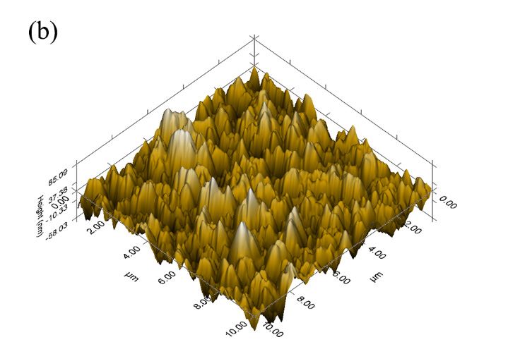
Materials 2018, 11, 1400                                                                                       3 of 13

      Table 1. Deposition parameters for TiN film fabricated by direct current magnetron sputtering (DCMS),
      HP + DC, and high power pulsed magnetron sputtering (HPPMS) modes.

                                                       Ti Inter-Layer             TiN Film
  Deposition       Distance to     Ratio of                                                         Deposition Rate
   Mode           Targets (mm)      Ar/N2         Time       Deposition    Time        Deposition     (nm/min)
                                                  (min)       Mode         (min)        Mode
       1                   150         160/18         5        DCMS          35         DCMS              62
       2                   150         160/18         5        HPPMS         35         DCMS              67
       3                   150         160/18         5        HPPMS         70         HPPMS             28

2.2. Film Characterization
      The surface and cross-sectional morphology of the samples were observed by scanning electron
microscopy (SEM, FEI 200, FEI, Hillsboro, OR, USA). The phase structure of the TiN films was
characterized by grazing incidence X-ray diffraction (GIXRD, Philips X’Pert Pro, PANalytical B.V.,
Almelo, Netherlands) with Cu Kα radiation and the incident angle of 0.5◦ , where the scan range
was from 30◦ to 80◦ . The Hardness and Young’s modulus of the deposited films were measured by
a nano-Indenter (Triboindenter, Hysitron 950, Bruker, Billerica, MA, USA) with a Berkovich head.
The test was applied with a load of 1 mN and depth of 90 nm. Then, the surface roughness of the TiN
films was measured by an atomic force microscope (AFM, Hysitron, Bruker, Billerica, MA, USA) fitted
to the indenter. The tribological test of the deposited films was performed on a ball-on-disc tribometer
(Tribo-S-D, CSM, Peseux, Switzerland). In this test, SiN balls (diameter of 6 mm) were selected as
friction pairs. The balls were under a constant normal load of 1 N, while the discs were circumrotated
at a certain speed to generate abrasion of the films (detailed in Table 2). The scratch adhesion tests
were performed on a Micro Combi Tester (Anton Parr, Graz, Austria), where the loading rate was
18 N/min and the progressive speed was 4 mm/min. Then, the scratch length was 3 mm. The tester
was fitted with acoustic emission monitoring equipment, which can detect emission in the vicinity of
100 kHz. Scratches were examined by optical microscopy (OM, VHX-1000C, KEYENCE, Osaka, Japan)
correlated with the acoustic emission observations to determine the cracking behavior and the critical
loads (Lc).

                                       Table 2. Parameters of the tribological test.

                       Tribology Pair       Load (g)      Speed (r/min)     Radius of Balls (mm)
                           Φ6 mm SiN            100             160                      4

     The corrosion behavior of DU and TiN coated DU samples were studied by potentiodynamic
polarization techniques on an electrochemical workstation (PARSTAT2263, Ametek, San Diego, CA,
USA). All of the electrochemical measurements were conducted using a conventional three-electrode
electrochemical cell in aerated neutral NaCl solution with 50 µg/g Cl− at room temperature with
the specimen as working electrode, a platinum plate as counter electrode, and a saturated calomel
electrode (SCE) as reference. The scan rate of potentiodynamic polarization was 0.2 mV/s.

3. Results and Discussion

3.1. Surface Morphology and Microstructure
    The surface morphologies of TiN film by different deposition modes are shown in Figure 1.
The TiN film that was deposited by DCMS mode shows large micro particles with voids between
each particle. While the film fabricated by HP + DC mode appears flattened and it interconnects
with no presence of voids. In the case of HPPMS mode, the film presents the most compact and
smoothest surface.
3.1. Surface Morphology and Microstructure
        The surface morphologies of TiN film by different deposition modes are shown in Figure 1.
 The TiN film that was deposited by DCMS mode shows large micro particles with voids between
 each particle. While the film fabricated by HP + DC mode appears flattened and it interconnects with
 no presence
Materials 2018, 11,of voids. In the case of HPPMS mode, the film presents the most compact and smoothest
                    1400                                                                             4 of 13
 surface.

  Materials 2018, 11, x FOR PEER REVIEW                                                                          4 of 13

       Figure 1. The surface morphology of TiN film by different deposition modes: (a) DCMS (b) HP + DC
     Figure 1. The surface morphology of TiN film by different deposition modes: (a) DCMS (b) HP + DC
       (c) HPPMS.
     (c) HPPMS.

       Further, AFM was used to characterize the surface morphology of the deposited TiN films
      Further,
  (Figure        AFM
           2), and        was usedsurface
                     the averaged     to characterize
                                             roughness (R the   surface
                                                            a) of         morphology
                                                                  the samples              of theaccordingly
                                                                                 was calculated    deposited (Table
                                                                                                                 TiN films
                                                                                                                       3).
(Figure 2), and
  The grain    sizethe
                     of averaged   surface
                        TiN decreased       roughness
                                          gradually      (RaDCMS
                                                      from   ) of themode
                                                                       samples    was
                                                                              (~0.4    calculated
                                                                                     μm)  to HPPMS accordingly
                                                                                                       mode (~0.3 (Table
                                                                                                                    μm).3).
The  grain mode
  HPPMS     size ofwillTiNcreate
                            decreased
                                 a high gradually     from DCMS
                                         ionization degree             mode
                                                               of target       (~0.4 µm)
                                                                         materials,   whichtocauses
                                                                                              HPPMS      mode (~0.3
                                                                                                     increased   adatomµm).
HPPMS
  energymode      will create
           and mobility         a high
                            on the      ionization
                                    substrate         degree
                                               surface,  andof    target materials,
                                                                subsequently           which
                                                                                 promotes   thecauses
                                                                                                 small increased   adatom
                                                                                                        grain migration
energy
  to theand
         grainmobility    on the
                 boundaries    andsubstrate   surface, migration
                                    grain boundary      and subsequently
                                                                     to hence promotes     the
                                                                                the refining    small
                                                                                             grain     grain
                                                                                                    sizes.    migration
                                                                                                            The TiN film to
  bygrain
the   DCMS     mode has and
           boundaries        the roughest   surface with
                                 grain boundary            Ra of 46.65
                                                      migration           nm,the
                                                                    to hence    while  the film
                                                                                    refining     by the
                                                                                              grain       HPPMS
                                                                                                     sizes.        mode
                                                                                                             The TiN   film
  presents  the   smoothest    surface  with  R   of 25.89 nm.   This  evolution   can  be
by DCMS mode has the roughest surface with Ra of 46.65 nm, while the film by the HPPMS mode
                                                a                                          attributed   to the enhanced
  ion bombardment
presents  the smoothest   andsurface
                               subsequently
                                       with Rahigher    surface
                                                  of 25.89        energy
                                                           nm. This        of the growing
                                                                        evolution            films. Besides,
                                                                                     can be attributed         the
                                                                                                          to the   larger
                                                                                                                 enhanced
  quantity
ion          of Ar+ ion
    bombardment          andbombardment
                              subsequentlyathigher
                                                 highersurface
                                                         bias voltage
                                                                  energyalso    resulted
                                                                           of the  growingin enhanced     etching
                                                                                              films. Besides,      oflarger
                                                                                                                 the  the
  asperities  and  + thus  smoothing   the  surface.
quantity of Ar ion bombardment at higher bias voltage also resulted in enhanced etching of the
asperities and thus smoothing the surface.
by DCMS mode has the roughest surface with Ra of 46.65 nm, while the film by the HPPMS mode
presents the smoothest surface with Ra of 25.89 nm. This evolution can be attributed to the enhanced
ion bombardment and subsequently higher surface energy of the growing films. Besides, the larger
quantity of Ar+ ion bombardment at higher bias voltage also resulted in enhanced etching of the
asperities
    Materialsand
             2018, thus   smoothing the surface.
                   11, 1400                                                                5 of 13

Materials 2018, 11, x FOR PEER REVIEW                                                                  5 of 13

        Figure
     Figure     2. Atomic
             2. Atomic    force
                       force    microscope(AFM)
                             microscope     (AFM)images
                                                  images of
                                                          of TiN
                                                             TiN film
                                                                 film by
                                                                      by (a)
                                                                         (a) DCMS;
                                                                             DCMS;(b)
                                                                                   (b)HP
                                                                                       HP+ +DC;
                                                                                             DC;and,
                                                                                                 and, (c)
        (c) HPPMS mode.
     HPPMS mode.

         Table 3.   Surface roughness (Ra ), hardness and Young’s modulus of TiN film by different
     Table 3. Surface roughness (Ra), hardness and Young’s modulus of TiN film by different deposition
        deposition modes.
     modes.
                       Deposition Mode       DCMS           HP + DC         HPPMS
                     Deposition Mode           DCMS           HP + DC          HPPMS
                                           46.65 ± 11.27   37.14 ± 6.65    25.89 ± 5.29
                         RRaa (nm)
                              (nm)
                                           46.65 ± 11.27 37.14 ± 6.65        25.89 ± 5.29
                       Hardness (GPa)       15.75 ± 0.41   20.56 ± 0.76    22.09 ± 0.39
                      Hardness   (GPa)
                       Modulus (GPa)        15.75±±2.21
                                           163.62    0.41 200.37
                                                            20.56±±   0.76 220.21
                                                                    4.17     22.09  ± 0.39
                                                                                  ± 2.33
                      Modulus (GPa)        163.62 ± 2.21 200.37 ± 4.17 220.21 ± 2.33

    Figure 3 presents the cross-sectional morphology of TiN film obtained by different deposition
modes. The thickness of the as-deposited film was 4~4.7 μm. The film morphology was evaluated
using the well-known structure zone models (SZM) (Figure 4) [18]. The film by DCMS mode presents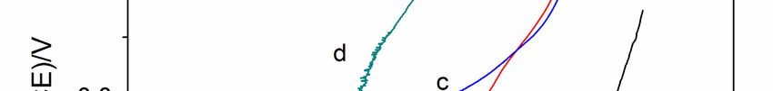
Materials 2018, 11, 1400                                                                                        6 of 13

      Figure 3 presents the cross-sectional morphology of TiN film obtained by different deposition
modes. The thickness of the as-deposited film was 4~4.7 µm. The film morphology was evaluated
using the well-known structure zone models (SZM) (Figure 4) [18]. The film by DCMS mode presents
a porous columnar morphology, which is the typical model of ZONE I. Due to the limited surface
diffusion, the atoms that were deposited on the substrate failed to diffuse into the bulk. Hence, the film
is consisted of uninterrupted fibrous columns, which exhibits porous and rough morphologies [19].
The HPPMS deposited film exhibits a rather denser columnar morphology identified by model of
ZONE T. A high level energy of ion bombardment will enhance the surface diffusion, which gives
rise to a different crystallographic orientation of grains, and therefore leads to a competitive growth.
The structure mode of HP + DC deposited film is between the modes of ZONE I and T. The abundance
of Ti+ ions in the Ti interlayer deposition flux during the HPPMS deposition will improve the transfer
to the growth surface to a certain extent. However, in the subsequent DCMS mode where the majority
of theMaterials
       ion flux    consists of the much lower energy Ar+ , the surface diffusion was limited. 6 of 13
                2018, 11, x FOR PEER REVIEW

            Figure 3. Cross-section morphology of TiN film grown by: (a) DCMS (4.7 μm); (b) HP + DC (4.7 μm);
      Figure 3. Cross-section morphology of TiN film grown by: (a) DCMS (4.7 µm); (b) HP + DC (4.7 µm);
           and, (c) HPPMS (4 μm).
      and, (c) HPPMS (4 µm).
Figure 3. Cross-section morphology of TiN film grown by: (a) DCMS (4.7 μm); (b) HP + DC (4.7 μm);
Materials 2018, 11, 1400                                                                               7 of 13
      and, (c) HPPMS (4 μm).

                                             The structure
                                   Figure 4. The
                                   Figure        structure zone model (SZM) [18].
Materials 2018, 11, x FOR PEER REVIEW                                                                                7 of 13

      GIXRD
      GIXRD measurements
                measurements were  were performed
                                         performed on   on TiN
                                                             TiN films
                                                                   films and
                                                                           and the
                                                                                the corresponding
                                                                                      corresponding XRD XRD patterns
                                                                                                               patterns are
                                                                                                                         are
shown
shown in  inFigure
             Figure5.5.Figure
                         Figure5a5aexhibits a strong
                                     exhibits  a strong(200)   orientation,
                                                            (200)  orientation,weak   (220)(220)
                                                                                    weak     orientation, and scarce
                                                                                                  orientation,         (111)
                                                                                                                and scarce
orientation.   FigureFigure
(111) orientation.     5b presents   a mixture
                               5b presents       of moreof
                                             a mixture       pronounced      (200) orientation
                                                               more pronounced                   with less with
                                                                                       (200) orientation    (111) less
                                                                                                                   and (111)
                                                                                                                       (220)
orientation.   Figure   5c exhibits  (111) preferred    orientation.    It is proposed     that
and (220) orientation. Figure 5c exhibits (111) preferred orientation. It is proposed that the  the competition    between
surface
competitionenergy   and strain
                between          energy
                            surface      during
                                     energy   and film
                                                   straingrowth
                                                             energymight
                                                                      during  contribute
                                                                                 film growthto the  changes
                                                                                                 might        in preferred
                                                                                                         contribute   to the
orientation
changes in preferred orientation [20]. The preferred orientation of film has an important effect on[21].
               [20].  The   preferred  orientation   of   film  has   an   important    effect  on  its performance       its
As  reported, [21].
performance      the preferred    orientation
                       As reported,             of (111)
                                      the preferred         plane is of
                                                      orientation      the(111)
                                                                            most    closely
                                                                                 plane       packed
                                                                                         is the        and it exhibits
                                                                                                most closely   packed andthe
lowest   strain
it exhibits  theenergy,
                  lowest while
                           strain (200) exhibits
                                  energy,   while the
                                                   (200)lowest    surface
                                                           exhibits          free energy
                                                                      the lowest     surface[22,23]. In the [22,23].
                                                                                              free energy    DCMS mode,
                                                                                                                      In the
the applied   substrate   temperature   is so
DCMS mode, the applied substrate temperature  low  (T s =  453  K)  that  the  surface  energy   controlled  the
                                                                is so low (Ts = 453 K) that the surface energy   growth    of
the TiN filmthe
controlled     and   the (200)
                   growth    of preferred  orientation
                                the TiN film   and thefavors      [22]. In theorientation
                                                           (200) preferred       case of HPPMSfavorsmode,
                                                                                                       [22].the
                                                                                                             In abundance
                                                                                                                the case of
of Ti + ion bombardment increased +the adatom mobility and diffusivity, thereby improving the strain
HPPMS mode, the abundance of Ti ion bombardment increased the adatom mobility and diffusivity,
energy,
therebywhich      facilitated
           improving           the preferred
                        the strain             orientation
                                    energy, which              of (111)
                                                     facilitated     the [23].
                                                                          preferred orientation of (111) [23].

      Figure 5. Grazing incidence X-ray diffraction (GIXRD) of TiN film deposited by three modes:
      Figure 5. Grazing incidence X-ray diffraction (GIXRD) of TiN film deposited by three modes: (a) DCMS
      (a) DCMS
      (b) HP + DC(b)(c)
                     HP  + DC (c) HPPMS.
                        HPPMS.

3.2. Hardness (H) and Young’s Modulus (E)
3.2. Hardness (H) and Young’s Modulus (E)
     Hardness and Young’s modulus values of the film deposited by different modes are listed in
     Hardness and Young’s modulus values of the film deposited by different modes are listed
Table 3. The hardness of HPPMS film (H = 20.56 GPa) was higher as compared to that of DCMS film
in Table 3. The hardness of HPPMS film (H = 20.56 GPa) was higher as compared to that of
(H = 15.75 GPa), and the hardness of HP + DC film (H = 22.09 GPa) was between them. The Young’s
DCMS film (H = 15.75 GPa), and the hardness of HP + DC film (H = 22.09 GPa) was between them.
modulus exhibits a similar tendency. The enhanced hardness was attributed to both a dense
The Young’s modulus exhibits a similar tendency. The enhanced hardness was attributed to both a
microstructure without inter-columnar voids that were prepared during film growth in HPPMS
dense microstructure without inter-columnar voids that were prepared during film growth in HPPMS
discharge [24] and the fact that (111) is the hardest orientation in TiN [25].
discharge [24] and the fact that (111) is the hardest orientation in TiN [25].
3.3. Wear Behavior
      The wear behavior of the TiN films was evaluated by pin-on-disc tests. Figure 6 plots the film
friction coefficient against sliding time, and then Table 4 shows the corresponding average tribology
coefficient (μ) of TiN film. It can be identified that the DCMS TiN has the highest wear coefficient
(μ = 0.56). The film by HP + DC mode exhibits a reduced friction coefficient (μ = 0.42). While, the
Materials 2018, 11, 1400                                                                                          8 of 13

3.3. Wear Behavior
     The wear behavior of the TiN films was evaluated by pin-on-disc tests. Figure 6 plots the
film friction coefficient against sliding time, and then Table 4 shows the corresponding average
tribology coefficient (µ) of TiN film. It can be identified that the DCMS TiN has the highest wear
coefficient (µ = 0.56). The film by HP + DC mode exhibits a reduced friction coefficient (µ = 0.42).
While, the HPPMS deposited one has a further improved wear resistant (µ = 0.34) when compared to
the two modes described above.

                           Table 4. The average tribology coefficient of three deposition modes.

                                        Deposition mode                 1        2        3
                                   Average tribology coefficient       0.56     0.42     0.34
     Materials 2018, 11, x FOR PEER REVIEW                                                                   8 of 13

     Article

     TiN Films Deposited on Uranium by High Power
     Pulsed Magnetron Sputtering under
     Low Temperature
          wear. Figure 7b presents a relatively light and narrow grooves with tiny debris, suggesting that
     the wear mechanism is dominated by abrasive wear in HP + DC mode. Meanwhile, the film by
     HPPMS mode exhibits a smooth surface with the lightest grooves (Figure 7c), identified by abrasive
     wear. The optical images are in good agreement with the friction coefficient results, which proves
     that the film deposited by HPPMS mode possesses excellent tribological characteristics.

                         Figure
                      Figure 6. 6.
                                TheThe  filmfriction
                                     film     frictioncoefficient
                                                       coefficient against
                                                                   against sliding
                                                                            slidingtime
                                                                                     timebyby
                                                                                            three modes.
                                                                                              three modes.

          The wear tracks of TiN films by three modes were observed by optical microscopy (OM). Deep
      Thewide
     and   weargrooves
                  tracks ofwith
                             TiNsome
                                  filmsobvious
                                        by threedebris
                                                    modes   were
                                                          were     observed
                                                                formed        by film
                                                                         on the  optical
                                                                                       by microscopy
                                                                                          DCMS mode(OM).      Deep
                                                                                                        (Figure 7a), and
widewhich
       grooves
             indicates that abrasive wear occurred accompanied by adhesion wear. Figure 7b presents a 7a),
                   with   some   obvious     debris    were  formed    on   the  film  by  DCMS     mode   (Figure
which   indicates
     relatively      that
                 light  andabrasive
                              narrowwear     occurred
                                       grooves           accompanied
                                                  with tiny               by adhesion
                                                              debris, suggesting     that wear.  Figure
                                                                                          the wear       7b presents
                                                                                                     mechanism    is a
relatively  light and  narrow    grooves   with   tiny  debris, suggesting   that  the wear
     dominated by abrasive wear in HP + DC mode. Meanwhile, the film by HPPMS mode exhibits amechanism    is dominated
by abrasive    wear inwith
     smooth surface      HP the
                              + DC   mode.
                                 lightest    Meanwhile,
                                          grooves    (Figure the
                                                             7c), film by HPPMS
                                                                  identified         modewear.
                                                                             by abrasive    exhibits a smooth
                                                                                                The optical     surface
                                                                                                             images
withare
      theinlightest
             good agreement
                      grooves with    the friction
                                (Figure             coefficient
                                          7c), identified    byresults,
                                                                 abrasivewhich  proves
                                                                             wear.   Thethat the film
                                                                                          optical     deposited
                                                                                                  images   are inby
                                                                                                                  good
     HPPMSwith
agreement      modethepossesses
                         frictionexcellent  tribological
                                  coefficient             characteristics.
                                                results, which    proves that the film deposited by HPPMS mode
possesses excellent tribological characteristics.

                                                       Figure 7. Cont.
Materials 2018, 11, 1400 9 of 13
Materials 2018, 11, x FOR PEER REVIEW 2 of 7
Figure 7. The wear tracks for the films after ball on disc wear tests against SiN ball: (a) DCMS
Figure 7. The wear tracks for the films after ball on disc wear tests against SiN ball: (a) DCMS (b) HP +
(b) HP + DC (c) HPPMS.
DC (c) HPPMS.
The HP + DC mode provides high energy ion bombardment during the Ti interlayer growth,
which
The HPshows
+ DCa certain
modeimprovement in surface
provides high energyroughness, porosity, hardness,
ion bombardment during and
the adhesion strength,
Ti interlayer growth,
as compared to DCMS mode. Further, HPPMS-deposited TiN films show superior performance
which shows a certain improvement in surface roughness, porosity, hardness, and adhesion strength, in
structure and mechanical performance, therefore resulting in enhanced tribology resistance.
as compared to DCMS mode. Further, HPPMS-deposited TiN films show superior performance in
structure and mechanical performance, therefore resulting in enhanced tribology resistance.
3.4. Adhesion
3.4. Adhesion
To observe and quantify the adhesion strength of TiN film by different deposition modes,
progressive micro-scratch tests were performed under the same condition (applied normal load
To observe and quantify the adhesion strength of TiN film by different deposition modes,
increased linearly from 0 to 10 N). The optical micrographs of scratches TiN film by different modes
progressive micro-scratch tests were performed under the same condition (applied normal load
after scratch test are shown in Figure 8 and the generated acoustic emission signals during scratch
increased
test are shown from
linearly 0 to 10
in Figure 9. N). The optical
It suggests that micrographs
TiN films thatofwere
scratches TiN film
deposited withby different
mode 1 andmodes
2
afterexperienced
scratch testsimilar
are shown in Figure
failure modes 8[26].
andIntheDCMS
generated
TiN, acoustic
the angularemission
cracks signals duringobserved
were clearly scratch test
are shown
initiatingin from
Figure the9.edge
It suggests
of scratchthat
at TiN
a veryfilms
lowthat
loadwere
of 4 deposited withnew
N. Then, some mode 1 andcracks
angular 2 experienced
were
similar
constantly being produced along the edge of scratch as the load progressed. The angle between thefrom
failure modes [26]. In DCMS TiN, the angular cracks were clearly observed initiating
angular
the edge of crack
scratchand atthe forward
a very lowdirection
load of 4ofN. theThen,
diamondsome scribing head was
new angular almostwere
cracks maintained
constantlyat 45°.
being
At the along
produced load ofthe 5.5edge
N, the ofsigns
scratchof chipping
as the load appeared at the The
progressed. area angle
between the angular
between crack and
the angular the and
crack
edge of scratch
the forward fromof
direction film-substrate
the diamond interface.
scribing The results
head was show that maintained
almost the film-substrate
at 45interface
◦ . At theclose
load of
5.5 N, the signs of chipping appeared at the area between the angular crack and thea edge
to the edge of scratch was damaged with the appearance of angular crack and failed at critical
ofload
scratch
of 5.5 N. While, the pre-deposition treatment of Ti interlayer using HP has a positive effect on
from film-substrate interface. The results show that the film-substrate interface close to the edge
adhesion strength of the TiN film by improving the critical load to almost 8 N. The TiN film that was
of scratch was damaged with the appearance of angular crack and failed at a critical load of 5.5 N.
produced by HPPMS mode shows completely different failure modes under the same conditions.
While, the pre-deposition treatment of Ti interlayer using HP has a positive effect on adhesion strength
There were no angular cracks observed in Figure 8c. The semi-circular brittle cracks formed at the
of the
rearTiN film
of the by improving
indenter (Figure 8c) theincritical
response load to tensile
to the almoststresses
8 N. ThethatTiN film that was
are generated during produced
sliding, by
HPPMS mode shows completely different failure modes under the same conditions. There were no
angular cracks observed in Figure 8c. The semi-circular brittle cracks formed at the rear of the indenterMaterials 2018, 11, 1400 10 of 13
(Figure 8c) in response to the tensile stresses that are generated during sliding, which played as typical
failure throughout the remaining process until spalling occurs at the load of 16 N. Obviously, the HP
deposition mode improved the scratch resistance of TiN film significantly, which may also attribute to
the enhanced ion bombardment during the HPPMS mode, which may make metal ions implanted and
incorporated in the
Materials 2018, 11, x substrate, and hence has an enhancement on interface.
FOR PEER REVIEW 10 of 13
FigureFigure 8. optical
8. The The optical micrographs
micrographs ofofscratches
scratches TiN film
filmby
bydifferent
differentmodes
modesafter scratch
after test: (a)
scratch DCMS
test: (a) DCMS
(b) HP + DC (c)
(b) HP + DC (c) HPPMS. HPPMS.Materials 2018,
Materials 11, x1400
2018, 11, FOR PEER REVIEW 11of
11 of 13
13
Figure
Figure 9. The acoustic
9. The acoustic emission
emissionsignals
signalsgenerated
generatedbyby TiN
TiN film
film with
with different
different modes
modes during
during scratch
scratch test:
test: (a) DCMS
(a) DCMS (b)+HP
(b) HP DC+ (c)
DCHPPMS.
(c) HPPMS.
3.5.
3.5. Corrosion
Corrosion Resistance
Resistance
Figure
Figure 1010 presents
presents thethe potentiodynamic
potentiodynamic polarization
polarization curves
curves of of DU
DU and and the
the DU
DU coated
coated with
with TiN
TiN
by different modes in aerated 50 ug/g NaCl solution and Table
by different modes in aerated 50 ug/g NaCl solution and Table 5 summarizes the corresponding5 summarizes the corresponding
electrochemical corrosionparameters.
electrochemical corrosion parameters.AAhighly highlyactive
active dissolution
dissolution behavior
behavior withwith regard
regard to the
to the barebare
DU
DU was observed in curve a. Above the corrosion potential (Ecorr),
was observed in curve a. Above the corrosion potential (Ecorr), the anodic current density increased the anodic current density
increased
sharply and sharply and itreached
it finally finally reached the limiting
the limiting current current density
density of approximately
of approximately 3.43.4 × 10
× 10 A/cm22..
−6−6A/cm
TiN
TiN films
films could
couldprevent
preventDU DUfromfrom rapid
rapid corrosion,
corrosion, as demonstrated
as demonstrated by curve
by curveb, c, b,
d. Especially, all of
c, d. Especially,
the TiN films were characterized by a passive region. However, the current
all of the TiN films were characterized by a passive region. However, the current density (icorr) density (icorr) of HPPMS
TiN (2.6 × 10TiN
of HPPMS
−8 A/cm2) was lower
(2.6 × 10⁻⁸ A/cm by an orderlower
2 ) was of magnitude
by an orderthan of that of HP + DCthan
magnitude TiNthat
(2.7 ×of10HP
−7 A/cm2)
+ DC
and two orders − 7of magnitude
2 than that of DCMS TiN (5.1 × 10 −7
TiN (2.7 × 10 A/cm ) and two orders of magnitude than that of DCMS TiN (5.1 × 10 A/cm A/cm 2 ), respectively. As reported,
− 7 the
2 ),
electrochemical resistance of film is strongly related to the microstructure and
respectively. As reported, the electrochemical resistance of film is strongly related to the microstructure surface morphology
[11,27]. The relatively
and surface morphology lower corrosion
[11,27]. resistancelower
The relatively of thecorrosion
DCMS TiN film is mainly
resistance of the DCMSdue to TiNits porous
film is
columnar structure so that the solution can easily reach the DU substrate
mainly due to its porous columnar structure so that the solution can easily reach the DU substrate via the pinholes. The denser
via
structure in HP
the pinholes. The + DC TiNstructure
denser films contributes
in HP + DC to the
TiNenhanced electrochemical
films contributes resistance
to the enhanced as compared
electrochemical
to DCMS TiN.
resistance In addition,
as compared HPPMS
to DCMS TiN. TiN provides
In addition, a competitive
HPPMS TiN provides growth structure with
a competitive growthfewstructure
defects
and the lowest porosity, which accounts for the best corrosion resistance.
with few defects and the lowest porosity, which accounts for the best corrosion resistance.
Figure
Figure 10.
10. Potentiodynamic
Potentiodynamic polarization
polarization curves
curvesof
of DU
DU substrate
substrateand
and TiN
TiN films
films by
by different
different modes:
modes:
(a) DCMS, (b) HP ++ DC, (c) HPPMS,
DC, (c) HPPMS, and (d) depleted uranium (DU).Materials 2018, 11, 1400 12 of 13
Table 5. The electrochemical corrosion parameters of DU and DU coated with TiN by different modes:
(a) DCMS, (b) HP + DC, and (c) HPPMS in aerated 50 ug/g NaCl solution.
Deposition Mode Ecorr (mV) Icorr (A/cm2 )
DU −773 ± 97 3.4 ± 0.7 × 10⁻⁶
DCMS −230 ± 21 5.1 ± 3.8 × 10⁻⁷
HP + DC −113 ± 14 2.7 ± 1.4 × 10⁻⁷
HPPMS −87 ± 19 2.6 ± 1.1 × 10⁻⁸
4. Conclusions
In this study, TiN film has been deposited on DU under low temperature by direct current
magnetron sputtering (DCMS) and high power pulsed magnetron sputtering (HPPMS), respectively.
The experimental results shown in this work demonstrate that the HPPMS deposited TiN film
exhibited a compact and smooth surface as compared to DCMS that was deposited TiN. The DCMS
deposited TiN films exhibited porous columnar structure, which corresponds to zone I in the
well-known structure zone model (SZM); while, the HPPMS counterpart shows competitive texture
growth, which corresponds to zone T in SZM. The preferred orientation of DCMS produced TiN films
changed from (200) to (111) with HPPMS. The HPPMS fabricated TiN film reveals a high hardness of
22.09 GPa, Young’s modulus of 220.21, low friction coefficient of 0.34, high adhesion of Lc 16 N, and an
improved corrosion resistance. Besides, the process of Ti interlayer deposition by HPPMS can enhance
the film properties as compared to DCMS, which is attributed to the enhanced ion bombardment
during the HPPMS.
In summary, the results that are shown in this work prove that the TiN film deposited by HPPMS
on DU could significantly improves its mechanical, tribological and corrosion performance and
therefore serves as a promising surface protective coating for DU.
Author Contributions: J.D. analyzed the electrochemical data and wrote the manuscript, X.Y. and X.M. performed
the measurements on the properties, L.F. contributed to the supervision of research, checked and polished the
manuscript, A.Y. performed the experiments on the sample preparation and co-wrote the manuscript.
Funding: This work is support by the National Science Foundation of China (Grant Nos. 11702261 and 61604138),
the Discipline Development Foundation of China Academy of Engineering and Physics (Grant Nos. 2015B0301065
and Nos. 2015B0302061) and the Strategic High-Tech Key Project (Grant No. BGX2016010304).
Conflicts of Interest: The authors declare no conflict of interest.
References
1. McGillivray, G.W.; Geeson, D.A.; Greenwood, R.C. Studies of the kinetics and mechanism of the oxidation of
uranium by dry and moist air A model for determining the oxidation rate over a wide range of temperatures
and water vapor pressures. J. Nucl. Mater. 1994, 208, 81–97. [CrossRef]
2. Toque, C.; Milodowski, A.E.; Baker, A.C. The corrosion of depleted uranium in terrestrial and marine
environments. J. Environ. Radioact. 2014, 128, 97–105. [CrossRef] [PubMed]
3. Orman, S.; Owen, L.W.; Picton, G. The corrosion behaviour of nickel-plated uranium. Corros. Sci. 1972, 12,
35–44. [CrossRef]
4. Liu, K.Z.; Luo, L.Z.; Zhou, W. Study of behaviors of aluminum overlayers deposited on uranium via aes,
eels, and xps. Appl. Surf. Sci. 2013, 270, 184–189. [CrossRef]
5. Liu, T.W.; Dong, C.; Wu, S. TiN, TiN gradient and Ti/TiN multi-layer protective coatings on Uranium.
Surf. Coat. Technol. 2007, 201, 6737–6741. [CrossRef]
6. Zhu, S.F.; Chen, L.; Wu, Y.P. Microstructure and corrosion resistance of Cr/Cr2 N multilayer film deposited
on the surface of depleted uranium. Corros. Sci. 2014, 82, 420–425. [CrossRef]
7. Arkush, R.; Mintz, M.H.; Shamir, N. Passivation of uranium towards air corrosion by N2+ and C+ ion
implantation. J. Nucl. Mater. 2000, 281, 182–190. [CrossRef]
8. Arkush, R.; Mintz, M.H.; Shamir, N. Long-term amorphisation of C+ and N2+ implanted layers on a uranium
surface. J. Alloys Compd. 2002, 330, 472–475. [CrossRef]Materials 2018, 11, 1400 13 of 13
9. Wang, Y.T.; Lin, Y.C. Study on the Performance of Nano-Titanium Nitride-Coated Stainless Steel Electrodes
in Electro-Fenton Systems. Nanomaterials 2018, 8, 494. [CrossRef] [PubMed]
10. Mori, T.; Fukuda, S.; Takemura, Y. Improvement of mechanical properties of Ti/TiN multilayer film deposited
by sputtering. Surf. Coat. Technol. 2001, 140, 122–127. [CrossRef]
11. Shukla, K.; Rane, R.; Alphonsa, J.; Maity, P.; Mukherjee, S. Structural, mechanical and corrosion resistance
properties of Ti/TiN bilayers deposited by magnetron sputtering on AISI 316L. Surf. Coat. Technol. 2017, 324,
167–174. [CrossRef]
12. Håkansson, G.; Hultman, L.; Sundgren, J.-E.; Greene, W.-D.; Munz, W.-D. Microstructures of TiN films grown
by various physical vapour deposition techniques. Surf. Coat. Technol. 1991, 48, 51–67. [CrossRef]
13. Al Jabbari, Y.S.; Fehrman, J.; Barnes, A.C.; Zapf, A.M.; Zinelis, S.; Berzins, D.W. Titanium Nitride and
Nitrogen Ion Implanted Coated Dental Materials. Coatings 2012, 2, 160–178. [CrossRef]
14. Perillo, P.M. Corrosion behaviour of titanium nitride coating on Titanium and Zircaloy-4. Am. J. Mater. Sci.
Appl. 2015, 3, 18–25.
15. Konstantinidis, S.; Ricard, A.; Ganciu, M. Measurement of ionic and neutral densities in amplified magnetron
discharges by pulsed absorption spectroscopy. J. Appl. Phys. 2004, 95, 2900–2905. [CrossRef]
16. Kouznetsov, V.; Macák, K.; Schneider, J.M. A novel pulsed magnetron sputter technique utilizing very high
target power densities. Surf. Coat. Technol. 1999, 122, 290. [CrossRef]
17. Ehiasarian, A.P.; Münza, W.-D.; Hultman, L.; Helmersson, U.; Petrov, I. High power pulsed magnetron
sputtered CrNx films. Surf. Coat. Technol. 2003, 163–164, 267–272. [CrossRef]
18. Barna, P.B.; Adamik, M. Fundamental structure forming phenomena of polycrystalline films and the structure
zone models. Thin Solid Films 1998, 317, 27–33. [CrossRef]
19. Sarakinos, K.; Alami, J.; Konstantinidis, S. High power pulsed magnetron sputtering a review on scientific
and engineering. Surf. Coat. Technol. 2010, 204, 1661–1684. [CrossRef]
20. Chawla, V.; Jayaganthan, R.; Chandra, R. Structural characterizations of magnetron sputtered nanocrystalline
TiN thin films. Mater. Charact. 2008, 59, 1015–1020. [CrossRef]
21. Abadias, G. Stress and preferred orientation in nitride-based pvd coatings. Surf. Coat. Technol. 2008, 202,
2223–2235. [CrossRef]
22. Pelleg, J.; Zevin, L.Z.; Lungo, S. Reactive-sputter-deposition TiN films on glass substrates. Thin Solid Films
1991, 197, 117–128. [CrossRef]
23. Greene, J.E.; Sundgren, J.; Hultman, L. Development of preferred orientation in polycrystalline TiN layers
grown by ultra high vacuum reactive magnetron sputtering. Appl. Phys. Lett. 1995, 67, 2928–2930. [CrossRef]
24. Paulitsch, J.; Mayrhofer, P.H.; Münz, W.D. Structure and mechanical properties of CrN/TiN multilayer
coatings prepared by a combined HIPIMS/UBMS deposition technique. Thin Solid Films 2008, 517, 1239–1244.
[CrossRef]
25. Wu, J.; Wu, B.H.; Ma, D.L. Effects of magnetic field strength and deposition pressure on the properties of
TiN films produced by high power pulsed magnetron sputtering (HPPMS). Surf. Coat. Technol. 2017, 315,
258–267. [CrossRef]
26. Bull, S.J. Failure modes in scratch adhesion testing. Surf. Coat. Technol. 1991, 50, 25–32. [CrossRef]
27. Gharagozloo, P.E.; Kanouff, M.P. Ionic diffusion oxidation model of uranium. J. Am. Ceram. Soc. 2013, 96,
2943–2949. [CrossRef]
© 2018 by the authors. Licensee MDPI, Basel, Switzerland. This article is an open access
article distributed under the terms and conditions of the Creative Commons Attribution
(CC BY) license (http://creativecommons.org/licenses/by/4.0/).You can also read