USB-2020 12-bit, 20 MS/s, Simultaneous Sampling, Ultra High-Speed USB Board - Logicbus
←
→
Page content transcription
If your browser does not render page correctly, please read the page content below
USB-2020
12-bit, 20 MS/s, Simultaneous Sampling, Ultra High-Speed USB Board ¡ Tu Sitio de Automatización !
Features
• Two 20 MS/s analog inputs
−− Simultaneous sampling
−− 1 A/D per channel
−− 12-bit resolution
−− ±10 V, ±5 V, ±2 V, ±1 V voltage
ranges (software-selectable)
−− 17 MHz input bandwidth
• 64 megasample onboard memory
−− 40 MS/s overall rate to onboard
memory when acquiring from
both channels
−− 8 MS/s throughput to host
computer
• Analog and digital triggering
−− Level and edge
• Analog and digital gating
• Internal or external pacing of
analog scans The USB-2020 offers high-speed simultaneous sampling at rates up to 20 MS/s per channel
• Eight digital I/O lines to onboard memory.
• BNC connectors and 40-pin auxilia-
ry connector for signal connections Overview BURSTIO
• Includes USB cable1, power The USB-2020 is a high-speed two-chan- BURSTIO enables a device to acquire
supply (required), and nylon stand- nel data acquisition board that provides data at higher rates than are supported
offs simultaneous sampling at rates up to by the USB data transfer rate.
• Small, compact design (7.1” x 5.6”) 20 MS/s per channel. Users can sample
for OEM and embedded applications data from both channels at an overall In BURSTIO, the USB-2020 can sample
rate of 40 MS/s to the 64 megasample data to onboard memory at rates up to
Software onboard memory, or continuously 20 MS/s per channel.
• Universal Library includes sup- stream data to a host computer at up to
port for Visual Studio® and Visual 8 MS/s for one or both channels over a Because each channel has its own A/D
Studio® .NET, including examples high-speed USB connection. converter, an overall sample rate of
for Visual C++®, Visual C#®, Visual 40 MS/s is achieved when sampling both
Basic®, and Visual Basic® .NET Each channel has its own A/D converter channels. The simultaneous sampling
• InstaCal software utility for install- for simultaneous sampling to eliminate eliminates channel skew and maintains
ing, configuring, and testing channel skew and ensure phase informa- phase coherence between the two chan-
• ULx for NI LabVIEW™ tion between channels is maintained. nels.
• TracerDAQ® software for acquiring
and displaying data and generating Flexible triggering and gating ensures The memory buffer can store up to
analog signals data is acquired when needed. The 64 megasamples at the maximum rate
• Supported Operating Systems: clock I/O input allows acquisitions to be for transfer to the computer after the
Windows® 8/7/Vista®/XP, 32-bit or controlled by the onboard clock or by acquisition is complete.
64-bit an external clock source for applications
that require user-supplied pacing.
Continuous Scan Mode
The board provides signal connections Continuous scan mode enables data to
through four standard BNC connectors be directly transferred to the host com-
and a 40-pin auxiliary connector. puter during acquisition. The maximum
rate in continuous scan mode is 8 MS/s
for all acquired data (one channel or two
Analog Input Acquisition channels). The maximum rate achieved
depends on the host computer.
Modes
1 The included USB cable has a higher gauge The USB-2020 can acquire analog data
wire (24 AWG minimum VBUS/GND, 28 AWG using BURSTIO or continuous scan
minimum D+/D–) than generic USB cables, and is
required for proper enumeration.
mode.
soporte@logicbus.com www.logicbus.com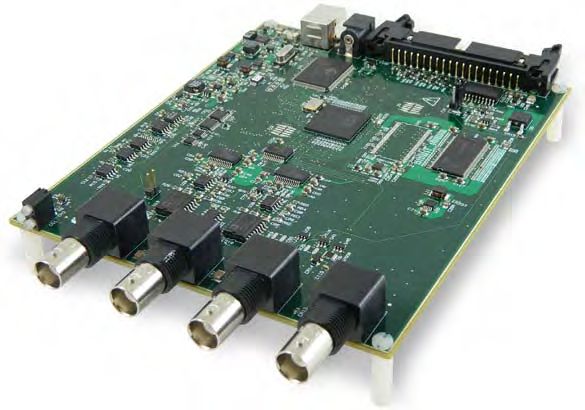
USB-2020
General Information

                                                     USB-2020 Block Diagram

                                                                                        Each analog channel has
                                                                                        a dedicated A/D converter
                                        1 Gb                                                   A/D 0
                                                                A/D Data                                                     CH0
                                        FIFO                                            12     20 MS/s

                                                                                                A/D 1                        CH1
                                                                                        12      20 MS/s

                                 Microprocessor                 A/D Data
          USB                                                                                        TRIG                    TRIG IN
                                                                                                    Control
                                                                      FPGA

                                                                                                   Clock I/O                 CLK IO

                                                         15 V
                                                        –15 V

                                       Power             5 VA
                                                                                          8            DIO
                                                        –5 VA
                                       System
                                                        3.3 V
                                                        2.5 V
                                                        1.2 V

External Clock I/O                                                   Digital I/O
USB-2020 analog input scanning operations can be paced with          The USB-2020 provides eight digital I/O lines on the 40-pin
the internal A/D clock or with an external clock source.             auxiliary connector. When a bit is configured for input, it can
                                                                     detect the state of any TTL-level input.
The CLK IO connector can be configured through software
for input (default) for external pacing, or for output to pace a     Each DIO channel is an open-drain, which can sink up to
connected device.                                                    150 mA for direct drive applications when used as an output.

Trigger Input                                                        External Pull-Up Capability
The USB-2020 supports digital and analog triggers and gates,         Digital inputs are pulled high by default to 5 V through
and each type has software-selectable configurations.                47 kΩ resistors on the circuit board. The pull-up voltage is
                                                                     common to all 47 kΩ resistors. The pull-up/pull-down state
•   Digital triggers can be configured for rising or falling edge,   can be changed from a header on the board.
    or for high or low level.
                                                                     An external pull-up resistor can also be used to pull the DIO
•   Analog triggers can be configured for above or below
                                                                     bit up to a voltage that exceeds the internal 5 V pull-up volt-
    software-selectable level, or for rising or falling edge with
                                                                     age (15 V maximum).
    software-selectable hysteresis.
•   Digital gates can be configured for high or low level.
•   Analog gates can be configured for software-selectable high
    or low level, or for in or out of software-selectable window.
An analog scan can have a trigger or a gate, but not both. For
example, an analog trigger cannot be used at the same time as
the TRIG IN BNC connector is being used to gate.

                soporte@logicbus.com                                                                      www.logicbus.com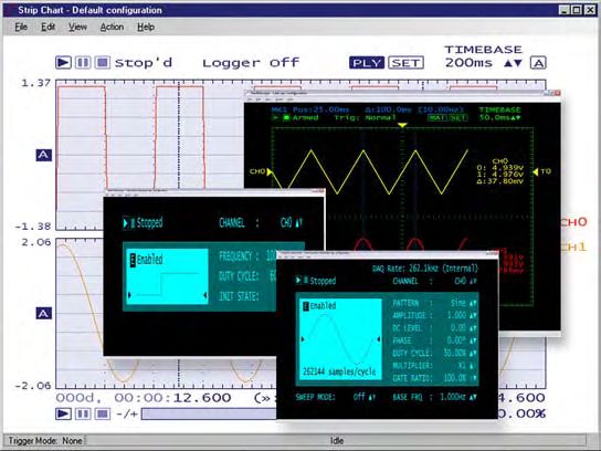
USB-2020
General Information

BNC and 40-Pin Auxiliary Connectors
The USB-2020 provides four standard BNC connectors for both
analog inputs, trigger input, and clock I/O. Use standard BNC
cables to connect the BNC female connectors.

The board also includes a 40-pin auxiliary connector for the
eight digital I/O, two 5 V power outputs, and an alternate trig-
ger input connection. The signals available from the 40-pin
auxiliary connector require a separately-purchased cable.

Cables and Accessories for Field Wiring and
Signal Termination
Use the following cables and accessories to connect to the
signals available from the 40-pin auxiliary connector:

•   C40FF-x: This 40-conductor ribbon cable can connect the
    40-pin auxiliary connector to a CIO-MINI40 universal
    screw-terminal board to terminate field signals and route        TracerDAQ provides four virtual instrument applications used to
    them into the USB-2020.                                          graphically display and store input data.
•   C40-37F-x: This 40-pin connector can connect the 40-pin
    auxiliary connector to a CIO‑MINI37 universal screw-ter-         Universal Library
    minal board or SCB-37 signal connector box to terminate          The Universal Library (UL) is a set of programming libraries
    field signals and route them into the USB-2020                   for developing applications with Visual Studio programming
                                                                     languages (and others) for use with Measurement Computing
DAQ Software                                                         hardware. UL includes a complete function library that simpli-
The USB-2020 ships with the DAQ software CD, which                   fies the configuration and operation of your measurement
includes InstaCal, a software utility for installing, calibrating,   device. UL supports Visual Studio and Visual Studio .NET, and
and testing .                                                        includes 64-bit driver support for Windows 8/7/Vista/XP.

                                                                     ULx for NI LabVIEW
                                                                     ULx for NI LabVIEW is a comprehensive library of graphical
                                                                     functions and example programs comprising all the power
                                                                     of the Universal Library and InstaCal. ULx for NI LabVIEW is
TracerDAQ                                                            compatible with NI LabVIEW 8.5 and later, and allows quick
TracerDAQ is an out-of-the-box application that can generate,        development of NI LabVIEW instrumentation, acquisition,
acquire, analyze, display, and export data within seconds of         and control applications .
installing data acquisition hardware.
TracerDAQ includes a strip chart, an oscilloscope, a func-
tion generator, and a rate generator, all of which are accessed
through a common, easy-to-use interface.                             Software Available Separately
                                                                     TracerDAQ Pro
                                                                     TracerDAQ Pro is available as a purchased upgrade to
                                                                     TracerDAQ. TracerDAQ Pro supports more active channels,
                                                                     more samples per channel, and a selection of options and
                                                                     enhancements designed to address many test and measure-
                                                                     ment applications.

               soporte@logicbus.com                                                                    www.logicbus.com
USB-2020
Specifications
Specifications Noise Performance
For the peak-to-peak noise distribution test, a single-
Drain to Source Breakdown Voltage: 42.5 V min
(does not include the additional leakage current
All specifications are subject to change without contribution that can occur when using an exter-
ended input channel is connected to AGND at the
notice. Typical at 25 °C unless otherwise specified. nal pull-up resistor)
input BNC connector and 20,000 data samples are
acquired at the maximum rate. Off State Leakage Current: 1.0 µA
Analog Input Sink Current Capability: 150 mA max (continu-
Range Counts LSBrms ous) per output pin; 150 mA max (continuous),
A/D Converter Type: AD9225
total for all eight channels
Number of Channels: 2 ±10 V 5 0.76 DMOS Transistor On-Resistance
Resolution: 12-bits
±5 V 5 0.76 (Drain to Source): 4 Ω
Input Configuration: Single-ended, individual A/D
per channel
±2 V 7 1.06 External Trigger
Sampling Method: Simultaneous
Input Ranges: ±10 V, ±5 V, ±2 V, ±1 V, software- ±1 V 7 1.06 Trigger Source
selectable Digital: TRIG IN on BNC connector and 40-pin
Connection Type: BNC connector)
Input Coupling: DC Analog Input Calibration Analog: CH0 or CH1
Absolute Maximum Input Voltage: ±15 V max Trigger Mode
Recommended Warm-Up Time: 15 minutes min
(power on) Digital: Rising or falling edge, high or low level
Calibration Method: Self calibration, with calibra-
Input Impedance: 1.5 MΩ typ Analog: Trigger above or below software-select-
tion factors for each range stored onboard in
Input Leakage Current: 2 uA typ, 10 uA max able level, rising or falling edge with software-
non-volatile memory
Input Bandwidth (3 db): All input ranges, 17 MHz selectable hysteresis
Calibration Interval: 1 year (factory calibration)
typ A/D Gate Source
Crosstalk: DC to 10 kHz, –90 dB Digital: TRIG IN (BNC connector and 40-pin
Trigger Source Digital Input/Output connector)
Digital: TRIG IN (BNC connector or 40-pin con- Digital Type: CMOS Analog: CH0 or CH1
nector) Number of I/O: 8 A/D Gate Modes
See External Trigger for more information Configuration: Each bit can be independently Digital: High or low level
Analog: CH0 or CH1 configured as input (power on default) or output. Analog: Software-selectable high or low level, in
Sample Clock Source Input bits can be read at any time whether the or out of software-selectable window
Internal: 1 kHz to 20 MHz max digital output is active or tri-stated. Trigger Latency: 50 ns max
External: CLK IO (BNC connector) Input Voltage Range: 0 V to 15 V Trigger Pulse Width: 25 ns min
See External Clock Input/Output for more infor- Input Characteristics: 47 kΩ pull-up/pull-down Input Type: 49.9 Ω series resistor
mation resistor, 28 kΩ series resistor Input High Voltage: 2.0 V min
Throughput Abs. Maximum Input Voltage: +20 V max Input Low Voltage: 0.8 V max
Continuous Scan: 1 kS/s min to 8 MS/s max to Pull-Up/Pull-Down Configuration: The port has
host computer (maximum rate is system-depen- 47 kΩ resistors that can be configured as pull-up
dent) or pull-down with an internal jumper. The fac-
External Clock Input/Output
BURSTIO: 1 kS/s min to 20 MS/s max to 64 MS tory configuration is pull-up (J10 shorting block Terminal Name: CLK IO (BNC connector)
onboard memory default position is pins 1 and 2) Terminal Type: ADC clock input/output, software-
Signal-to-Noise Ratio (SNR): 66.6 dB Pull down capability is available by placing the J10 selectable for input or output (default is input)
Signal-to-Noise and Distortion Ratio (SINAD): shorting block across pins 2 and 3. Terminal Description: When configured for input,
66.5 dB Digital I/O Transfer Rate (Software Paced): 33 S/s receives sampling clock from external source
Spurious Free Dynamic Range (SFDR): 80 dB to 4,000 S/s typ; system-dependent When configured for output, outputs the internal
Total Harmonic Distortion (THD): 80 dB Input High Voltage: 2.0 V min sampling clock
Input Low Voltage: 0.8 V max Clock Rate: 1 kHz to 20 MHz max
Output Characteristics: 47 kΩ pull-up, open drain Stability: ±50 ppm
(DMOS transistor, source connected to ground) Input Impedance: 1 MΩ
Output Voltage Range: 0 V to 5 V (using 47 KΩ Input Threshold
internal pull up resistors); 0 V to 15 V max High: 2.0 V min
through optional, user-supplied external pull-up Low: 0.8 V max
resistors Maximum Rate: 20 MHz
Adding external pull-up resistors connects the Input Range: 0 V to 5.5 V
output bit in parallel with the internal 47 kΩ Clock Pulse Width: 25 ns min
pull-up resistor. The resulting load voltage Input Type: 49.9 Ω series resistor
depends on the value of the external resistor Input High Voltage: 2.0 V min
value and the pull-up voltage used. In general, Input Low Voltage: 0.8 V max
external 10 KΩ pull-up resistors are sufficient for Output High Voltage: 2.4 V min
most applications. Output Low Voltage: 0.4 V max
Output Current: 24 mA max
Accuracy
DC Accuracy Components and Specifications. All Values are (±)
Range Gain Error Offset Error INL Error Absolute Accuracy Gain Temperature Coefficient Offset Temperature
(% of reading) (mV) (% of range) at Full Scale (mV) (% reading/°C) Coefficient (µV/°C)
±10 V 0.11 5.2 0.0976 35.72 0.0035 30
±5 V 0.11 5.2 0.0488 20.46 0.0035 110
±2 V 0.11 1.1 0.0244 8.18 0.0035 10
±1 V 0.11 1.1 0.0122 4.64 0.0035 25
soporte@logicbus.com www.logicbus.comUSB-2020
Specifications & Ordering
Memory Ordering Information
Data FIFO: 64 MS using BURSTIO, 4 kS not using
BURSTIO Part No. Description
Non-Volatile Memory: 32 KB (30 KB firmware
USB-2020 Ultra high-speed, simultaneous sampling USB DAQ board with 2 SE analog inputs,
storage, 2 KB calibration/user data)
20 MS/s throughput to internal memory, analog/digital triggers and gates, clock I/O,
and 8 digital I/O lines. Includes power supply ( p/n CB-PWR-9), USB cable, and
Power standoffs.
Supply Voltage: 9 VDC to 20 VDC (only use
plug-in power supply - p/n CB-PWR-9)
Supply Current: 0.75 A max (this is the total qui-
escent current requirement for the device that
Accessories & Cables
includes up to 10 mA for the Status LED. This Part No. Description
value does not include potential loading of the
DIO bits or the +VO pin) C40FF-x 40-conductor ribbon cable, female to female (x = 1, 2, 3, 4, 5, 10, 15, 20, 25, and 50
Power Jack Configuration: Two conductor, barrel foot lengths)
Power Jack Barrel Diameter: 6.3 mm
Power Jack Pin Diameter: 2.0 mm CIO-MINI40 Universal 40-pin screw-terminal board, connects via a C40FF-x cable
Power Jack Polarity: Center positive
+VO Voltage Range: 4.50 V to 5.25 V
+VO Current Sourcing: 10 mA max. C40-37F-x 40-pin ribbon cable, female IDC to 37-pin female D shell (x = 1, 2, 3, 4, 5, 10, 15, 20,
25, and 50 foot lengths)
Environmental
CIO-MINI37 Universal 37-pin screw-terminal board, connects via a C40-37F-x cable
Operating Temperature Range: 0 °C to 50 °C max
Storage Temperature Range: –40 °C to 85 °C max
Humidity: 0% to 90% non-condensing max
SCB-37 Shielded 37-pin signal connection box, connects via a C40-37F-x cable
Mechanical
Dimensions (L × W × H): 142.24 × 180.34 × 38.09 mm
(5.6 × 7.1 × 1.5 in.)
Weight: 1.5 lb
USB
USB Device Type: USB 2.0 (high-speed)
Device Compatibility: USB 2.0
USB Cable Type: A-B cable, UL type AWM 2527 or
equivalent
(min 24 AWG VBUS/GND, min 28 AWG D+/D–)
USB Cable Length: 3 m (9.84 ft) max
Signal I/O Connectors
CIO-MINI37
USB: B type CIO-MINI40
Auxiliary Connector (J9): 40-pin header connector
Compatible Cables for the 40-Pin Auxiliary Con- SCB-37
nector: C40FF-x and C40-37F-x
Compatible Accessory Products with the C40FF-x
Cable: CIO-MINI40
Compatible Accessory Products with the Software
C40‑37F-x Cable: CIO-MINI37 and SCB-37
Part No. Description
BNC Connectors
TracerDAQ Pro Out-of-the-box virtual instrument suite with strip chart, oscilloscope, function
CH0: Analog input channel 0
generator, and rate generator – professional version
CH1: Analog input channel 1
TRIG IN: BNC connection for external digital
trigger (also available on the auxiliary
connector J9)
CLK IO: BNC connection for the ADC clock I/O,
software-selectable for input or output
soporte@logicbus.com www.logicbus.comYou can also read