Wireless Transmission at 0.3 THz Using Direct THz-to-Optical Conversion at the Receiver
←
→
Page content transcription
If your browser does not render page correctly, please read the page content below

Wireless Transmission at 0.3 THz Using Direct
THz-to-Optical Conversion at the Receiver
S. Ummethala(1,2),*, T. Harter(1,2), K. Koehnle(1,2), Z. Li(1), S. Muehlbrandt(1,2), Y. Kutuvantavida(1,2),
J. N. Kemal(1), J. Schaefer(3), H. Massler(4), A. Tessmann(4), S. K. Garlapati(5), A. Bacher(2), L. Hahn(2),
M. Walther(4), T. Zwick(3), S. Randel(1), W. Freude(1), C. Koos(1,2),**
(1)
Institute of Photonics and Quantum Electronics (IPQ), Karlsruhe Institute of Technology (KIT), Karlsruhe, Germany,
*
sandeep.ummethala@kit.edu, **christian.koos@kit.edu
(2)
Institute of Microstructure Technology (IMT), Karlsruhe Institute of Technology (KIT), Karlsruhe, Germany
(3)
Institute of Radio Frequency Engineering & Electronics (IHE), Karlsruhe Institute of Technology (KIT), Karlsruhe, Germany
(4)
Fraunhofer Institute for Applied Solid State Physics (IAF), Freiburg, Germany
(5)
Institute of Nanotechnology (INT), Karlsruhe Institute of Technology (KIT), Karlsruhe, Germany
Abstract We report a THz wireless link at 0.2885 THz which is embedded in a photonic network. An
ultra-broadband plasmonic modulator directly converts the THz signal to the optical domain. We transmit
QPSK data with line rates up to 50 Gbit/s.
Introduction conversion of a THz wireless data signal to an
Wireless networks have to cope with an exponen- optical carrier without prior down-conversion to
tial increase in mobile data traffic, which is pre- the baseband or an intermediate frequency.
dicted1 to account for 63 % of the global internet
Plasmonic-organic hybrid (POH) modulator
traffic by 2021. To meet the underlying capacity
In our experiment, T/O conversion is
challenges, wireless communication networks
accomplished by an ultra-broadband POH Mach-
will have to handle data rates of tens or even hun-
Zehnder modulator7,8 (MZM), which is fabricated
dreds of Gbit/s per link. This can only be accom-
on the standard silicon-on-insulator (SOI)
plished by exploiting frequency windows of low
2 platform with a device layer thickness of 220 nm,
atmospheric attenuation in unallocated spectral
see Fig 1. Each arm of the MZM comprises a
ranges beyond 0.275 THz. From a networking
metallic nanoslot of 75 nm width that forms a
perspective, future wireless links need to be inti-
plasmonic slot waveguide of length L between
mately integrated into fiber-optic infrastructures,
gold electrodes, Fig. 1(a). A pair of silicon (Si)
which calls for seamless connection of optical fi-
waveguide tapers (blue) allow conversion
bers to THz transmitter (Tx) and receiver (Rx)
between the Si photonic mode and the tightly
front-ends. At the Tx, optoelectronic conversion
confined plasmonic mode (Fig. 1(a), inset on top
of data streams from the optical to the THz do-
right) in the metallic slot. The RF signal coupled
main has been demonstrated to offer a variety of
3 through the ground-signal-ground contacts of the
advantages such as wideband tunability of the
MZM drops in the metallic nanoslot (Fig. 1(a),
carrier frequency and the ability to exploit ad-
inset on bottom left), leading to a strong overlap
vanced modulation formats and multiplexing
between the optical and RF electric fields. The
schemes that are widely used in state-of-the-art
modulator is functionalized by filling the slot with
optical communications. As an example, wireless
an electro-optic (EO) cladding material (SEO100
transmission at 100 Gbit/s has previously been
4 from Soluxra, LLC). The active chromophores are
demonstrated by direct optical-to-THz (O/T) con-
aligned (green arrows in Fig 1(b)) through a one-
version of a wavelength-division multiplexing
time poling process by applying a DC electric field
(WDM) signal in an ultra-fast uni-travelling-carrier
U pol at an elevated temperature. The modulating
photodiode (UTC-PD). In contrast to that, direct
electrical drive voltage U d in Fig. 1(c) is oriented
THz-to-optical (T/O) conversion of data signals
(red arrows) parallel to the chromophore
has not yet been shown.
alignment in one arm of the MZM and antiparallel
In this paper, we demonstrate a wireless link
in the other one, leading to a push-pull operation
that is seamlessly integrated into a photonic net-
of the MZM. Plasmonic modulators are predicted
work, exploiting direct O/T and T/O conversion at
to have operating bandwidths8 up to 1 THz as the
the Tx and the Rx. The wireless link operates at
slot capacitance (~ 3 fF) is connected to the
a carrier frequency of 0.2885 THz with a maxi-
50 signal source through a highly conductive
mum line rate of 50 Gbit/s, bridging a distance of
metal film leading to a large RC corner frequency.
16 m. The THz signal is generated by O/T con-
In a recent experiment9, we demonstrated a flat
version in a UTC-PD. At the receiver, the THz sig-
frequency response of POH MZM up to at least
nal is converted to the optical domain by using an
0.325 THz as shown in Fig. 1(c).
ultra-broadband plasmonic-organic hybrid (POH)
modulator5,6. The POH modulator has a footprint Experimental Setup
of only 500 µm2 and is suitable for high-density The fiber-to-fiber link consists of an O/T con-
integrated photonic circuits. To the best of our verter, the wireless link and a T/O converter,
knowledge, this is the first demonstration of direct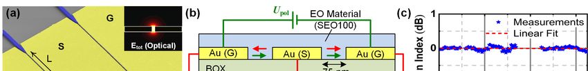
Fig. 1: Plasmonic-organic hybrid (POH) modulator. (a) Colorized scanning electron micrograph of POH Mach-Zehnder modulator
(MZM) showing two plasmonic slot waveguides of length L between ground-signal-ground (GSG) electrodes. Tapers are used at
the transisions between the silicon photonic strip waveguides and the plasmonic section, enabling efficient conversion between
the photonic and the plasmonic modes. Mode profiles of the optical quasi-TE field (top right) and the RF/THz field (bottom left)
showing strong confiment to the metallic slot. (b) Cross-section of POH MZM. During the poling process, a DC voltage Upol (green)
is applied across the floating ground pads at an elevated temperature, thereby aligning the EO chromophores (green arrows)
with respect to the applied field. The orientation of the dipoles is retained after cooling down the device. A modulating drive
voltage Ud (red) across the MZM induces fields (red arrows) parallel to the EO chromophore orientation in one arm, and
antiparallel in the other arm of the MZM leading to a push-pull operation. (c) Frequency response of POH MZM.
Fig. 2(a,b). A schematic of the O/T converter is the-art metamorphic high electron mobility tran-
depicted in Fig 2(a). An arbitrary-waveform gen- sistors11 (mHEMT). The THz power required to
erator (AWG, Keysight M9505A) with a sampling drive the plasmonic modulator can be reduced by
frequency of 90 GSa/s is used to generate a optimizing the poling procedure and using mate-
quadrature phase-shift keying (QPSK) data sig- rials with higher EO response, for which a figure
3
nal using a pseudo-random binary sequence of merit as large12 as nEO r33 2300pm/V has
(PRBS) with a length of 211-1. The electrical is been demonstrated in a silicon-organic hybrid
coupled to an IQ electro-optical modulator that (SOH) MZM. The received THz signal is amplified
modulates a continuous-wave (CW) carrier pro- in two stages – first by an H-band low-noise am-
vided by an external cavity laser (ECL) at a fre- plifier (LNA, 26 dB gain, 9 dB noise figure,
quency f 0 193.3THz . The IQ modulator is op- −30 dBm maximum input power) and then by an
erated at its null-point in order to supress the car- H-band medium-power amplifier (MPA, 15 dB
rier at f 0 . The modulated signal is superimposed gain, saturation output power +4 dBm) – before
with an unmodulated CW carrier at driving the POH MZM through a THz GSG probe
f Tx,LO 193.0115THz . Both optical waves are (GGB picoprobe Model 325B). The intensity-
photomixed in a UTC-PD10 that generates a mod- modulated output of the POH MZM is a T/O-con-
ulated THz carrier at the difference frequency, verted signal with modulation sidebands cen-
f Tx,THz f 0 f Tx,LO 0.2885THz . A conical tered around the optical carrier f Rx,LO . One of
horn antenna with a gain of 26 dBi radiates the the modulation sidebands ( f Rx,LO f Tx,THz ) is
QPSK-modulated THz carrier into free-space. A selected with a band-pass filter and is amplified
plano-convex THz lens made from polytetrafluo- to an optical power of 1 dBm before analyzing the
roethylene (PTFE) collimates the radiated beam. signal quality with a coherent receiver (Agilent
The THz receiver as shown in Fig 2(b) directly optical modulation analyzer N4391A, OMA). The
transfers the THz data signal onto an optical car- signal received by the OMA is post-processed
rier without prior down-conversion. The laser and equalized to evaluate the bit error ratio
power at a frequency f Rx,LO 194.57 THz is am- (BER).
plified by an erbium doped fiber amplifier (EDFA)
and is launched into the POH MZM through an Results and Discussion
An exemplary spectrum of the optical signal
on-chip grating coupler. The plasmonic modula-
feeding the UTC-PD is shown in Fig. 2(c). Here,
tor has a length L = 20 µm and a U L product of
a 15 GBd QPSK data stream was used to
240 V µm, resulting in a figure of merit
3
nEO r33 330pm/V . The QPSK modulated THz modulate a 193.3°THz carrier, which is photo-
wave from the transmitter is received by a combi- mixed with a CW laser tone at 193.0115°THz,
thereby transferring the signal to a carrier at
nation of lens and conical horn antenna that is
0.2885 THz. Fig. 2(d) shows the filtered lower
similar to the one used at the transmitter. In order
to compensate the free-space loss of the THz sig- sideband of the T/O converted intensity modu-
lated optical signal after the POH MZM. The
nal, a cascade of two millimeter-wave monolithic
measured BER of the T/O-converted signal for
integrated circuit (MMIC) amplifiers with a total
gain of 41 dB and a saturation output power of different symbol rates of the QPSK data is shown
in Fig. 2(e). The BER is below the threshold of
4 dBm is employed. The amplifiers use state-of-
forward-error correction (FEC) with a
Fig. 2: Demonstration of fiber-wireless-fiber link. (a) THz transmitter setup for O/T conversion: An arbitrary-waveform generator
(AWG) is used to modulate QPSK data on an optical carrier at f0 . The signal is then is superimposed with an unmodulated optical
carrier at f Tx,LO , amplified and photomixed in a uni-travelling-carrier photodiode (UTC-PD) to generate a QPSK signal on a THz
carrier. A horn antenna attached to the UTC-PD radiates the signal into free-space. A PTFE lens collimates the beam. (b) THz
receiver setup for T/O conversion: Light from a laser at a frequency f Rx,LO is amplified with an EDFA and coupled to a POH
MZM on a silicon chip through an on-chip grating coupler (GC). The THz data signal received by a PTFE lens and a horn antenna
is amplified by two H-band amplifiers (low-noise amplifier, LNA and medium-power amplifier, MPA) to drive the POH MZM for T/O
conversion. The intensity-modulated signal generated by the POH MZM is amplified, filtered (band pass filter, BPF) to supress
the carrier and one of the modulation sidebands, and analysed in an optical modulation analyser (OMA). (c) Optical spectrum
carrying 15 GBd QPSK data (inset) at 193.3 THz and a detuned CW tone for feeding the UTC-PD to generate a THz carrier at
0.2885 THz. (d) Filtered spectrum of 15 GBd QPSK signal (inset) up-converted to 194.286 THz by the POH MZM. The drop in the
power spectrum for the T/O-converted lower sideband at higher frequencies stems from the frequency-dependent gain of the THz
amplifiers. (e) Measured bit error ratio (BER) of the T/O-converted signal for different symbol rates of QPSK data.
7 % overhead for symbol rates up to 18 GBd (line                   References
rate of 36 Gbit/s). For the 25 GBd QPSK signal                     [1] "Cisco Visual Networking Index: Forecast and
with a line rate of 50 Gbit/s, we obtain a BER of                       Methodology, 2016-2021", White Paper (2017).
1.1×10⁻² which is below the threshold for soft-                    [2] ITU-R Rec. P.676-11, "Attenuation by atmospheric
                                                                        gases", (2016).
decision FEC with 20 % overhead.                                   [3] Nagatsuma, T. et. al., "Advances in terahertz
                                                                        communications accelerated by photonics", Nature
Summary                                                                 Photon. 10, 371–379 (2016).
We demonstrate for the first time a seamless in-                   [4] Koenig, S. et al. "Wireless sub-THz communication
tegration of a 0.2885 THz wireless link into a fi-                      system with high data rate". Nature Photon. 7, (2013).
ber-optic network. We exploit optical-to-THz con-                  [5] Melikyan, A. et al., "High-speed plasmonic phase
                                                                        modulators. Nature Photon. 8, 229–233 (2014).
version at the transmitter and direct THz-to-opti-                 [6] Haffner, C. et al., "All-plasmonic Mach–Zehnder
cal conversion at the receiver using an ultra-                          modulator enabling optical high-speed communication at
broadband       plasmonic      modulator.     We                        the microscale", Nature. Photon. 9, 525–528 (2015).
demonstrate the viability of the concept by                        [7] Melikyan, A. et al. "Plasmonic-organic hybrid (POH)
                                                                        modulators for OOK and BPSK signaling at 40 Gbit/s"
transmitting QPSK data signals with line rates up                       Optics Express 23, 9938 (2015).
to 50 Gbit/s over a distance of 16 m.                              [8] Koos, C. et al. "Silicon-Organic Hybrid ( SOH ) and
                                                                        Plasmonic Organic Hybrid (POH) Integration" J.
Acknowledgements                                                        Lightwave Technology. 34, 256–268 (2016).
We thank Jingdong Luo and Alex K.-Y. Jen from                      [9] Ummethala, S et.al., “Terahertz-to-Optical Conversion
                                                                        Using a Plasmonic Modulator”, Proc. CLEO, STu3D.4
Soluxra for providing the organic EO material. We                       (2018)
acknowledge support by the European Research                       [10] Ito, H. et. al., "Photonic millimetre- and sub-millimetre-
Council (ERC Starting Grant ‘EnTeraPIC’, s#                             wave generation using J-band rectangular- waveguide-
280145; ERC Consolidator Grant ‘TeraSHAPE’,                             output     uni-travelling-carrier   photodiode     module",
                                                                        Electron. Lett. 42, 1424–1425 (2006).
# 773248), by the Alfried Krupp von Bohlen und                     [11] Tessmann, A. et al., "High-gain submillimeter-wave
Halbach Foundation, by the Helmholtz Interna-                           mHEMT amplifier MMICs", IEEE MTT-S Int. Microw.
tional Research School for Teratronics (HIRST),                         Symp. Dig. 53–56 (2010).
and by the Karlsruhe Nano-Micro Facility                           [12] Kieninger, C et al., ” Ultra-high in-device electro-optic fig-
                                                                        ure of merit n3r33 = 2300 pm/V demonstrated in a silicon-
(KNMF).                                                                 organic hybrid (SOH) modulator”, arXiv: 1709.06338
                                                                        (2018).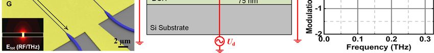


You can also read