EVAL-1ED32xxMC12H user guide - Infineon Technologies
←
→
Page content transcription
If your browser does not render page correctly, please read the page content below
UG-2021-25 EVAL-1ED32xxMC12H user guide Single channel, isolated, two -level, slew-rate control gate driver IC (2L-SRC) 1ED3241MC12H, 1ED3251MC12H About this document Scope and purpose The gate driver evaluation boards EVAL-1ED3241MC12H and EVAL-1ED3251MC12H feature the two-level, slew- rate control (2L-SRC) gate driver ICs 1ED3241MC12H and 1ED3251MC12H. This user guide demonstrates the functionality and key features of the Infineon EiceDRIVER™ 2L-SRC gate driver ICs. The gate driver ICs are certified according to UL 1577 and VDE 0884-11. The design of the evaluation board EVAL-1ED32x1MC12H was performed with respect to the environmental conditions described in this document. The design was tested as described in this document, but not qualified regarding manufacturing, lifetime or over the full range of ambient operating conditions. The boards provided by Infineon are not subject to full production tests. Evaluation boards are not subject to the same procedures as regular products regarding returned material analysis (RMA), process change notification (PCN) and product discontinuation (PD). Evaluation boards are intended to be used under laboratory conditions and by trained specialists only. Intended audience Engineers who want to learn how to use the Infineon EiceDRIVER™ 1ED3241MC12H and 1ED3251MC12H Experienced design engineers who design circuits with Infineon EiceDRIVER™ , IGBT and CoolSiC™ MOSFET Design engineers who develop power electronic devices, such as inverters Evaluation Board This board will be used during design in, for evaluation and measurement of characteristics, and proof of data sheet specifications. Note: PCB and auxiliary circuits are NOT optimized for final customer design. User guide Please read the Important notice and the Safety precautions and the Warnings Revision 1.0 www.infineon.com page 1 of 17 2021-05-28
EVAL-1ED32xxMC12H user guide
Single channel, isolated, two-level, slew-rate control gate driver IC (2L-SRC)
Important notice
Important notice
“Evaluation Boards and Reference Boards” shall mean products embedded on a printed circuit board
(PCB) for demonstration and/or evaluation purposes, which include, without limitation, demonstration,
reference and evaluation boards, kits and design (collectively referred to as “Reference Board”).

Environmental conditions have been considered in the design of the Evaluation Boards and Reference
Boards provided by Infineon Technologies. The design of the Evaluation Boards and Reference Boards
has been tested by Infineon Technologies only as described in this document. The design is not qualified
in terms of safety requirements, manufacturing and operation over the entire operating temperature
range or lifetime.

The Evaluation Boards and Reference Boards provided by Infineon Technologies are subject to functional
testing only under typical load conditions. Evaluation Boards and Reference Boards are not subject to the
same procedures as regular products regarding returned material analysis (RMA), process change
notification (PCN) and product discontinuation (PD).

Evaluation Boards and Reference Boards are not commercialized products, and are solely intended for
evaluation and testing purposes. In particular, they shall not be used for reliability testing or production.
The Evaluation Boards and Reference Boards may therefore not comply with CE or similar standards
(including but not limited to the EMC Directive 2004/EC/108 and the EMC Act) and may not fulfill other
requirements of the country in which they are operated by the customer. The customer shall ensure that
all Evaluation Boards and Reference Boards will be handled in a way which is compliant with the relevant
requirements and standards of the country in which they are operated.

The Evaluation Boards and Reference Boards as well as the information provided in this document are
addressed only to qualified and skilled technical staff, for laboratory usage, and shall be used and
managed according to the terms and conditions set forth in this document and in other related
documentation supplied with the respective Evaluation Board or Reference Board.

It is the responsibility of the customer’s technical departments to evaluate the suitability of the
Evaluation Boards and Reference Boards for the intended application, and to evaluate the completeness
and correctness of the information provided in this document with respect to such application.

The customer is obliged to ensure that the use of the Evaluation Boards and Reference Boards does not
cause any harm to persons or third party property.
The Evaluation Boards and Reference Boards and any information in this document is provided "as is"
and Infineon Technologies disclaims any warranties, express or implied, including but not limited to
warranties of non-infringement of third party rights and implied warranties of fitness for any purpose, or
for merchantability.

Infineon Technologies shall not be responsible for any damages resulting from the use of the Evaluation
Boards and Reference Boards and/or from any information provided in this document. The customer is
obliged to defend, indemnify and hold Infineon Technologies harmless from and against any claims or
damages arising out of or resulting from any use thereof.

Infineon Technologies reserves the right to modify this document and/or any information provided
herein at any time without further notice.

User guide                                          2 of 17                                        Revision 1.0
                                                                                                    2021-05-28
EVAL-1ED32xxMC12H user guide
Single channel, isolated, two-level, slew-rate control gate driver IC (2L-SRC)
Safety precautions
Safety precautions

Note:        Please note the following warnings regarding the hazards associated with development systems.

Table 1        Safety precautions
                        Warning: The DC link potential of this board is up to 600 VDC. When measuring voltage
                        waveforms by oscilloscope, high voltage differential probes must be used. Failure to do
                        so may result in personal injury or death.

                        Warning: The evaluation or reference board contains DC bus capacitors which take
                        time to discharge after removal of the main supply. Before working on the drive
                        system, wait five minutes for capacitors to discharge to safe voltage levels. Failure to
                        do so may result in personal injury or death. Darkened display LEDs are not an
                        indication that capacitors have discharged to safe voltage levels.
                        Caution: The heat sink and device surfaces of the evaluation or reference board may
                        become hot during testing. Hence, necessary precautions are required while handling
                        the board. Failure to comply may cause injury.

                        Caution: Only personnel familiar with the drive, power electronics and associated
                        machinery should plan, install, commission and subsequently service the system.
                        Failure to comply may result in personal injury and/or equipment damage.

                        Caution: The evaluation or reference board contains parts and assemblies sensitive to
                        electrostatic discharge (ESD). Electrostatic control precautions are required when
                        installing, testing, servicing or repairing the assembly. Component damage may result
                        if ESD control procedures are not followed. If you are not familiar with electrostatic
                        control procedures, refer to the applicable ESD protection handbooks and guidelines.
                        Caution: The evaluation or reference board is shipped with packing materials that
                        need to be removed prior to installation. Failure to remove all packing materials that
                        are unnecessary for system installation may result in overheating or abnormal
                        operating conditions.

User guide                                           3 of 17                                             Revision 1.0
                                                                                                          2021-05-28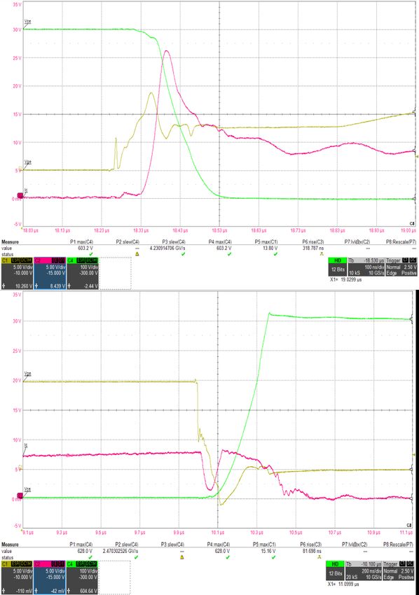
EVAL-1ED32xxMC12H user guide
Single channel, isolated, two-level, slew-rate control gate driver IC (2L-SRC)
Table of contents

Table of contents
About this document ....................................................................................................................... 1
Important notice ............................................................................................................................ 2
Safety precautions.......................................................................................................................... 3
Table of contents ............................................................................................................................ 4
1      The board at a glance .............................................................................................................. 5
1.1         Delivery content ...................................................................................................................................... 5
1.2         Block diagram.......................................................................................................................................... 6
1.3         Board parameters and technical data .................................................................................................... 6
2      System and functional description ........................................................................................... 8
2.1         Commissioning ........................................................................................................................................ 8
2.2         Overcurrent protection ........................................................................................................................... 9
2.3         Preparation for positive gate supply (0 – +15 V)..................................................................................... 9
3      System design.......................................................................................................................10
3.1         Schematics ............................................................................................................................................ 10
3.2         Layout .................................................................................................................................................... 10
3.3         Bill of material ....................................................................................................................................... 11
3.4         Connector details .................................................................................................................................. 12
4      System performance .............................................................................................................13
5      Appendices ...........................................................................................................................15
5.1         Abbreviations and definitions ............................................................................................................... 15
Revision history.............................................................................................................................16

User guide                                                                     4 of 17                                                                    Revision 1.0
                                                                                                                                                           2021-05-28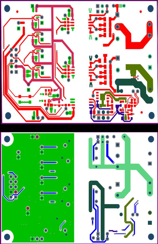
EVAL-1ED32xxMC12H user guide
Single channel, isolated, two-level, slew-rate control gate driver IC (2L-SRC)
The board at a glance
1 The board at a glance
This user guide (UG-2021-25) describes the evaluation board EVAL-1ED32x1MC12H that is intended for the
product feature evaluation of the Infineon EiceDRIVER Compact 1ED32x1MC12H in an application circuit. The
key elements of the board and the product are listed here.
Evaluation board in half-bridge configuration with two gate driver ICs to drive power switches such as IGBTs,
silicon MOSFETs and silicon-carbide (SiC) MOSFETs
Additional driver IC for ultra-fast, isolated, overcurrent feedback signaling from the high-voltage domain to
the logic control domain
Fast operational amplifier and comparator for ultra-fast overcurrent detection
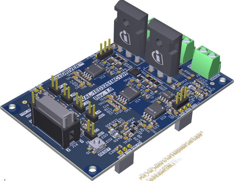
Figure 1 Evalboard EVAL-1ED3241MC12H (left) and EVAL-1ED3251MC12H (right)
This board is best suited for double-pulse testing. An additional high-voltage DC blocking capacitor at the high-
voltage supply is mandatory. The capacitor has to be placed as close as possible to the high-voltage supply
connectors. It requires additional considerations on thermal and power balance for continuous operation.
The control interface can be connected to a pulse generator, a microcontroller or other digital circuits.
For safe operation, a fast overcurrent detection and protection circuit is implemented with a galvanically
isolated feedback path to the low-voltage input-side. The input-side flip-flop latches the overcurrent event
information. This circuit will report the fault and turn off both gate driver ICs. The S1 button, also labeled with
RESET, clears the flip-flop to enable the gate driver ICs again.
1.1 Delivery content
The evaluation board EVAL-1ED3241MC12H contains the printed circuit board. This board is designed to feature
the 2L-SRC function for turn-on and turn-off. The assembled gate resistors are selected for use with
IKQ75N120CT2 and with gate supply of 0 - +15 V. However, the power transistors are not assembled.
The evaluation board EVAL-1ED3251MC12H contains the printed circuit board. This board is designed to feature
the 2L-SRC function for turn-on only. The assembled gate resistors are selected for use with IKQ75N120CT2 and
with gate supply of 0 - +15 V. However, the power transistors are not assembled.
User guide 5 of 17 Revision 1.0
2021-05-28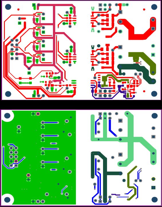
EVAL-1ED32xxMC12H user guide
Single channel, isolated, two-level, slew-rate control gate driver IC (2L-SRC)
The board at a glance

1.2            Block diagram

                                                Gate drive
                               Signal
                             interface

                                                Protection

Figure 2     Block diagram of EVAL-1ED32x1MC12H

1.3            Board parameters and technical data
The selected components on the evaluation boards, as well as the gate driver ICs, have maximum ratings and
operating conditions to avoid damaging the individual parts and the evaluation board overall.

Table 2      Absolute maximum ratings
 Pin/parameter          Connector        Min       Max         Unit    Note
 name
 +15V_IN                J15.2            -0.2      20          V       Input, if J16.10 is not connected;
                                                   100         mA      support supply voltage
 +15V                   J16.10           -0.2      20          V       Support supply voltage; input, if
                                                   100         mA      J15 is not connected; otherwise can
                                                                       be output
 INF_HS1, INF_LS1       J16.1, J16.2     -0.2      VCC1 +      V       Input, digital signal
                                                   0.2
 VCC1                   J16.3            -0.2      5.3         V       Input, gate driver IC supply voltage
 RST                    J16.5            -0.2      VCC1 +      V       Input, digital signal
                                                   0.2
 FAULT                  J16.6            -0.2      VCC1 +      V       Open drain output, digital signal
                                                   0.2
 IN_HS1, IN_LS1         J16.7, J16.8     -0.2      VCC1 +      V       Input, digital signal
                                                   0.2
 VCC2_HS,VCC2_LS        J6.3, J7.3,      -0.2      35          V       Overall isolated secondary supply
                        J11.3, J12.3                                   with reference to VEE2_HS/VEE2_LS
 VCC2_HS,VCC2_LS        J6.3, J7.3,      -0.2      20          V       Positive secondary supply voltage
                        J11.3, J12.3                                   with reference to
                                                                       GND2_HS/GND2_LS
 VEE2_HS,VEE2_LS        J6.2, J7.2,      -15       0.2         V       Gate reference supply pin with
                        J11.2, J12.3                                   reference to GND2_HS/GND2_LS
 V-HV                   J1               -0.2      800         V       Input, high-voltage supply, for
                                                                       voltages above 42 V, special high-
                                                                       voltage lab environment is strongly
                                                                       recommended

User guide                                         6 of 17                                          Revision 1.0
                                                                                                     2021-05-28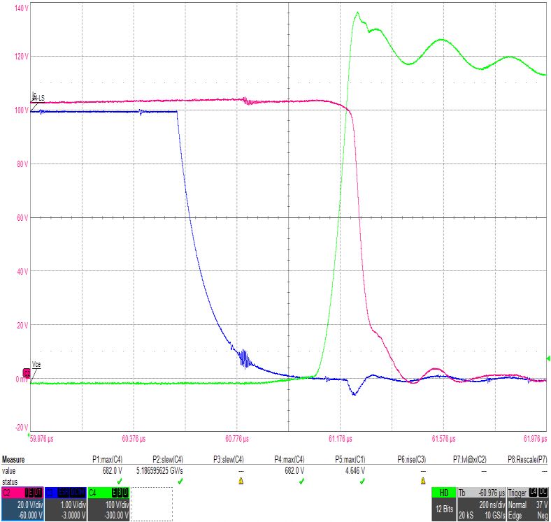
EVAL-1ED32xxMC12H user guide
Single channel, isolated, two-level, slew-rate control gate driver IC (2L-SRC)
The board at a glance

 Pin/parameter              Connector   Min            Max              Unit     Note
 name
 Phase peak current         J2          150            150              A        Phase peak current for double-
                                                                                 pulse tests
 tpulse                                 -              100              µs       Maximum ON pulse length for
                                                                                 double-pulse tests
 fsw                                    -              100              kHz      Maximum switching frequency for
                                                                                 continuous operation, careful
                                                                                 consideration of power dissipation
                                                                                 required for power transistor and
                                                                                 EiceDRIVER™ IC

The PCB assembly is optimized for a VCC1 supply voltage of 3.3 V. Higher supply voltages may require
adjustments to the current limiting resistors of the status LEDs.

Table 3      Operating conditions and supply voltages
 Pin name             Min.       Typ.   Max.       Unit          Note
 +15V_IN              15.5       16     16.5       V             Input, if J16.10 is not connected; support supply
                                                                 voltage
 +15V                 15.5       16     16.5       V             Support supply voltage; input, if J15 is not
                                                                 connected; otherwise can be output
 VCC1                 3.2        3.3    3.4        V             Input, gate driver IC supply voltage
 FAULT                -0.1       3.3    VCC1+0.1   V             Output, digital signal
 RST                  -0.1       3.3    VCC1+0.1   V             Input, digital signal
 IN_HS                -0.1       3.3    VCC1+0.1   V             Input, digital signal
 IN_LS                -0.1       3.3    VCC1+0.1   V             Input, digital signal
 VCC2_HS,VCC2_LS      12         15     20         V             Overall isolated secondary supply with reference
                                                                 to GND2_HS/GND2_LS
 VEE2_HS,             0          -      -15        V             Gate reference supply pin with reference to
 VEE2_LS                                                         GND2_HS/GND2_LS
 V-HV                 25         600    800        V             Input, high-voltage supply, referenced to HV_GND;
                                                                 for voltages above 42 V, special high-voltage lab
                                                                 environment is strongly recommended

Please note that the current into the supply terminals depends strongly on the operating conditions, such as
the switching frequency or the selected power transistor.

User guide                                             7 of 17                                                  Revision 1.0
                                                                                                                 2021-05-28
EVAL-1ED32xxMC12H user guide
Single channel, isolated, two-level, slew-rate control gate driver IC (2L-SRC)
System and functional description
2 System and functional description
2.1 Commissioning
Follow the steps below to set up and power up the board, and to perform first evaluations.
Prerequisites
Assemble fitting power switches at the location Q1 and Q2, e.g. IKQ75N120CT2 IGBTs
Assemble an external high-voltage DC capacitor (>330 µF) between J1-1/2 (V-HV) and J3-2 (HV_GND),
ensuring low stray inductance
Have low-voltage power supplies ready for input support and logic supply (+15V_IN, VCC1) with a current
capability of at least 100 mA for +15V_IN and 20 mA for VCC1
Have isolated low-voltage power sources ready for the gate drivers’ output supply (VCC2_HS - GND2_HS,
GND2_HS - VEE2_HS, VCC2_LS - GND2_LS, and GND2_LS - VEE2_LS). Each supply requires a curent capability
of 100 mA.
Have a high-voltage power supply ready for HV-DC between J1-1/2 (V-HV) and J3-2 (HV_GND)
Have an inductive load ready for double-pulse tests, e.g. 600 µH
Have a dual channel PWM generator ready for half bridge PWM input
To adapt the circuit to application requirements, resistor or capacitor values can be changed to optimize the
performance.
Power-up sequence
1. Connect supply GND to connector J15.1 and supply +15V_IN to connector J15.2 with +16 V.
2. Connect supply GND to connector J8.1 and supply VCC1 to connector J8.2 with +3.3 V.
3. The red LED3 will turn on.
4. Supply both secondary gate driver supplies with individual power sources at VCC2_HS - GND2_HS, and
GND2_HS - VEE2_HS at connector J6, and VCC2_LS - GND2_LS and GND2_LS - VEE2_LS at connector J7
according to the assembled power switch needs.
5. The green LED1 will turn on.
6. Connect the digital PWM generator to the digital interface connectors J16.7 and J16.8 labeled with IN_HS1
and GND as well as IN_LS1 and GND. Make sure that the outputs of the PWM generator are disabled, or the
signals are on low.
7. Connect the high-voltage supply to connector J1.1 or J1.2 and HV_GND to J3.2.
8. Connect one end of the inductive load to J2.1 and the other end according to the double-pulse
requirements to either J1.1 or J3.1 (low-side or high-side testing).
9. Push S1 to reset the error flip-flop.
10. The red LED3 will turn off and green LED2 will turn on.
11. The board is now ready for double-pulse evaluation.
Safe power-down sequence
1. Turn-off the DC-link voltage source and discharge the DC-link capacitor.
2. Check the DC-link voltage with e.g. a digital multimeter or an oscilloscope.
3. Turn-off the other supply voltages (VCC2, VEE2, +15_IN, VCC1).
User guide 8 of 17 Revision 1.0
2021-05-28EVAL-1ED32xxMC12H user guide
Single channel, isolated, two-level, slew-rate control gate driver IC (2L-SRC)
System and functional description
Figure 3 Connection of load for double-pulse tests
2.2 Overcurrent protection
The detection circuit measures the voltage across shunt resistor R22. This signal passes a RC filter R21
and C19 and comparator U5 compares it to a reference voltage. The reference voltage is defined by the
voltage divider R14 and R23. The trip value is at approximately 96 A, and can be adapted to application
requirements by changing the shunt resistor R22 and/or adapting the reference voltage divider R14
and R23.
The output signal is transferred with coupler U3 to the low-voltage domain to trigger the flip-flop and
store the overcurrent event. Once the flip-flop is triggered, the input signals of the logic AND gates U6 -
U9 are low. This turns off both IGBTs via the OUT terminal of the ICs U2 and U4. Thus the IGBTs are
turned off in the slow mode in case of EVAL-1ED3241MC12H. This can be compared to the soft turn-off
function of gate drivers, which contain an integrated short-circuit detection. In addition, it reports the
overcurrent event to the digital interface connector as a FAULT signal and turns the LED7 on.
EVAL-1ED3251MC12H does not contain the slow turn-off feature.
To return to normal operation, S1 needs to be pushed to reset the flip-flop. As feedback, LED7 turns off and
LED6 turns back on again.
2.3 Preparation for positive gate supply (0 – +15 V)
The board can be operated with output supply voltage of 0 - +15 V, too. Please apply a jumper on pins J6.1 and
J6.2. Furthermore, a jumper has to be applied on pins J7.1 and J7.2. Then, the output-side supply voltage can
be connected to pins J6.2, J6.3 and to pins J7.2 and J7.3, respectively.
User guide 9 of 17 Revision 1.0
2021-05-28EVAL-1ED32xxMC12H user guide
Single channel, isolated, two-level, slew-rate control gate driver IC (2L-SRC)
System design
3 System design
3.1 Schematics
The complete schematics are available on the download section of the Infineon homepage. A log-in is required
to download this material.
3.2 Layout
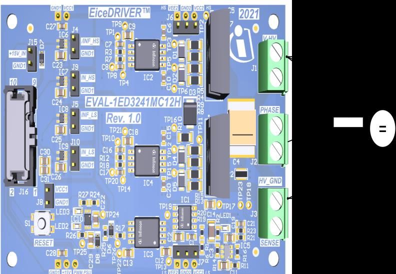
Figure 4 Top and bottom layer of Eval-1ED3241MC12H
User guide 10 of 17 Revision 1.0
2021-05-28EVAL-1ED32xxMC12H user guide
Single channel, isolated, two-level, slew-rate control gate driver IC (2L-SRC)
System design
Figure 5 Top and bottom layout of Eval-1ED3251MC12H
3.3 Bill of material
The complete bill of material is available on the download section of the Infineon homepage. A log-in is
required to download this material.
Table 4 BOM of the most important/critical parts of the evaluation or reference board
S. No. Ref Designator Description Manufacturer Manufacturer P/N
CAP, CERM, TDK B58031I9254M062
1 C4 0.25uF, 900V, 20%,
CeraLink
RES, 0R001, 5%, Isabellenhütte VLK-R001-5.0
1 R20
1W, 0612
User guide 11 of 17 Revision 1.0
2021-05-28EVAL-1ED32xxMC12H user guide
Single channel, isolated, two-level, slew-rate control gate driver IC (2L-SRC)
System design
3.4 Connector details
Table 5 Connectors and pin assignment
Connector Pin Marking/ Note
function
J1 1,2 V-HV High-voltage power supply
J2 1,2 PHASE
J3 1 SENSE Shunt resistor sense signal
2 HV_GND High-voltage reference signal
J4 1 GND High-side negative gate driver reference
2 INF_HS High-side gate driver input signal /INF
J5 1 GND High-side gate driver input signal IN
2 INF_HS High -side gate driver supply reference
J6, J7 (for direct supply 1 VEE2_HS High-side negative gate driver supply
only) 2 GND2_HS High-side gate driver supply reference
J11, J12 (for use with 3 VCC2_HS High-side positive gate driver supply
power supply unit only)
J8 1 GND Input-side gate driver supply reference
2 VCC1 Input-side gate driver supply
J9 1 GND Input-side gate driver supply reference
2 IN_HS High-side gate driver input signal IN
J10 1 GND Low-side positive gate driver supply
2 IN_HS Low-side gate driver input signal IN
J13 (for use with power 1 GND Input-side ground reference
supply unit only) 2 +15V External +15 V supply for power supply unit
3 PWM_PSU PWM signal for power supply unit
J14 (for use with power 1 GND Input-side ground reference
supply unit only) 2 VCC1 Input-side supply voltage, 3.3 V or 5 V
J15 1 GND Input-side ground reference
2 +15V_IN Input-side supply voltage +1 5 V
J16 1 INF_HS1 Input control signal high-side for slew-rate-control
2 INF_LS1 Input control signal low-side for slew-rate-control
3 VCC1 Input-side supply voltage
4 GND Input-side ground reference
5 RST Reset input signal
6 FAULT Fault (overcurrent) indication signal
7 IN_HS1 Input control signal high-side for PWM
8 IN_LS1 Input control signal low-side for PWM
9 PWM_PSU Input PWM signal for power supply unit
10 +15V External +15 V supply for power supply unit (if not
supplied through J15.2
User guide 12 of 17 Revision 1.0
2021-05-28EVAL-1ED32xxMC12H user guide
Single channel, isolated, two-level, slew-rate control gate driver IC (2L-SRC)
System performance
4 System performance
This section shows examples of switching waveforms using EVAL-1ED3241MC12H. The waveforms represent
turn-on and turn-off at a collector current of 7.5 A and a turn-off triggered by the overcurrent protection.
Figure 6 Turn-on (top) and turn-off (bottom) of IKQ75N120CT2 as low-side switch (VDC = 600 V, IC =
7.5 A, /INF = 1; yellow: VGE 5 V/div, red: IC 5 A/div, green: VCE,LS 100 V/div )
User guide 13 of 17 Revision 1.0
2021-05-28EVAL-1ED32xxMC12H user guide
Single channel, isolated, two-level, slew-rate control gate driver IC (2L-SRC)
System performance
Figure 7 Protection turn-off of IKQ75N120CT2 as low-side switch (VDC = 600 V, IC = 100 A, /INF = 1; red:
IC 20 A/div, blue: VIN 1 V/div, green: VCE,LS 100 V/div )
User guide 14 of 17 Revision 1.0
2021-05-28EVAL-1ED32xxMC12H user guide
Single channel, isolated, two-level, slew-rate control gate driver IC (2L-SRC)
Appendices
5 Appendices
5.1 Abbreviations and definitions
Table 6 Abbreviations
Abbreviation Meaning
CE Conformité Européenne
EMI Electromagnetic interference
UL Underwriters Laboratories
User guide 15 of 17 Revision 1.0
2021-05-28EVAL-1ED32xxMC12H user guide
Single channel, isolated, two-level, slew-rate control gate driver IC (2L-SRC)
Revision history
Revision history
Document Date of release Description of changes
version
Revision 1.0 2021-05-28 Initial version
User guide 16 of 17 Revision 1.0
2021-05-28Trademarks
All referenced product or service names and trademarks are the property of their respective owners.
For further information on the product, technology,
Edition 2021-05-28 delivery terms and conditions and prices please
Published by contact your nearest Infineon Technologies office
(www.infineon.com).
Infineon Technologies AG
81726 Munich, Germany WARNINGS
Due to technical requirements products may contain
dangerous substances. For information on the types
in question please contact your nearest Infineon
© 2021 Infineon Technologies AG. Technologies office.
All Rights Reserved.
Except as otherwise explicitly approved by Infineon
Do you have a question about this Technologies in a written document signed by
authorized representatives of Infineon
document? Technologies, Infineon Technologies’ products may
Email: erratum@infineon.com not be used in any applications where a failure of the
product or any consequences of the use thereof can
reasonably be expected to result in personal injury.
Document reference
UG-2021-25You can also read