A Self Threshold Voltage Compensated Rectifier for RF Energy Harvesting using 45nm CMOS Technology - WSEAS
←
→
Page content transcription
If your browser does not render page correctly, please read the page content below
WSEAS TRANSACTIONS on SYSTEMS
      DOI: 10.37394/23202.2021.20.27                                                     Chinmoy Bharali, Manash Pratim Sarma

 A Self Threshold Voltage Compensated Rectifier for RF Energy
           Harvesting using 45nm CMOS Technology
                                                 CHINMOY BHARALI
                                 Department of Electronics and Communication Engineering,
                                         Gauhati University Guwahati, INDIA

                                              MANASH PRATIM SARMA
                                 Department of Electronics and Communication Engineering
                                         Gauhati University, Guwahati, INDIA

Abstract— A high frequency rectifier is the core of a RF energy harvesting system. It should offer a very good efficiency at
low input power levels and to obtain that compensation of threshold voltage is a very important aspect. A threshold
compensation scheme for MOSFETS for RF rectifier applicable in RF energy harvesting system is presented in this paper.
The switching of the MOSFET is improved with overall enhancement of output rise time of the system. The design emphasis
is to have a simplified circuit without the requirement of any external source so as to achieve self-sustainability in the true
sense. The rectifier circuit is derived from the basic Dickson charge pump model and is evaluated using 45nm CMOS
process. The design has utilized Metal Oxide Semiconductor Field Effect Transistor instead of basic diodes which ensures
low power along with fabrication feasibility. The maximum measured PCE of the design is obtained to be 33% at 4dBm input
power level at 500Mhz frequency with 1 Kilo Ohm load resistance. The output transient response rise time has been
measured to be 85ns at 500MHz and 50.10ns at 1Ghz.
Keywords—Power Conversion Efficiency, Peak to Peak Voltage, Dickson Charge Pump, Threshold Value.
Received: March 24, 2021. Revised: July 18, 2021. Accepted: August 2, 2021. Published: August 10, 2021.

                                                                                 The overall performance of the RF energy
  1. Introduction                                                     harvesting system is based on the sensitivity and the overall
          Radio frequency (RF) energy harvesting is                   efficiency. The rectifier circuit is one of the main blocks that
becoming a very important research area in the advent of              is responsible for determining the overall performance of an
green communication. The basic idea of implementation of              RF harvesting system. Recently, there has been an increased
RF energy harvesting system is to avoid external batteries or         demand for highly-sensitive and highly-efficient rectifier
connection to any other power source [1,2,3]. This makes              circuits. Rectifier’s sensitivity is defined as the lower limit
the communication nodes self-sustainable in terms of power            input power level at which the rectifier is able to operate.
and eliminates the difficulties in remote locations. Among            The efficiency of a rectifier circuit indicates how well the
all other renewable sources RF energy harvesting is a                 rectifier is capable of converting the received RF power into
promising candidate with advantages of flexibility and                dc power along with self-loss of power in the rectifier.
portability. The RF energy harvesting system consists of a                       Design of a reconfigurable rectifier will also give a
receiving antenna, a RF rectifier to convert the RF energy            wide PCE response for a wide input power range. Gradually
into DC energy and a power management unit to manage the              increasing the efficiency of the RF EH system. In this paper,
harvested power. This is shown in figure 1. The output DC             the design of a reconfigurable rectifier with circuit-based
energy can be used by any load or can be stored in                    solution for threshold reduction of the devices is
capacitors or external batteries. With the advancement of             implemented. The maximum measured PCE of the design is
communication, along with faster and reliable data transfer           obtained to be 33% at 4dBm input power level at 500MHz
mechanisms, energy management and conservations are                   frequency with 1 Kilo Ohm load resistance. The output
getting more attention and is becoming a major and                    transient response rise time has been measured to be 85ns at
indispensable part of communication research. As self-                500MHz and 50.10ns at 1Ghz.Further details of the theory,
sustainability to communication nodes is a very important             design, and experimental results for the circuit are given in
aspect, RF energy harvesting must play a powerful role.               following sections.

                                                                        2. Proposed Design
                                                                      2.1 The Charge Pump
                                                                          The rectifier plays a signification role in the RFEH
                                                                      system. So, the prime objective of this work is to develop a
                                                                      rectifier with faster response time that is to develop certain
                                                                      technique for effective threshold compensation and better
                                                                      conversion efficiency. Fig. 2 shows the circuit schematic of
                                                                      a single stage Dickson charge pump. In order to find the
   Figure 1: Block diagram of a RF energy harvesting system           optimum device sizes a single stage Dickson charge pump
                                                                      [10] was examined.

      E-ISSN: 2224-2678                                         244                                            Volume 20, 2021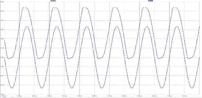
WSEAS TRANSACTIONS on SYSTEMS
DOI: 10.37394/23202.2021.20.27 Chinmoy Bharali, Manash Pratim Sarma
the positive phase which results in providing a alternating
bias voltage to trigger the M1 device of the charge pump.
3. Experiment Results
3.1 Comparator output voltage
In Fig. 4 the output voltage waveform of the comparator
Figure 2: Dickson Charge Pump circuit with reference to RF input signal is shown is shown.
V(n006) is the output of the comparator and V(n002) is the
A single-stage Dickson charge pump rectifier consists of input RF signal.
two NMOS transistors, M1 and M2, one coupling capacitor
(Cc), and one multiplying/output capacitor (Co). The RF It is observed from the figure above that the comparator
signal is applied to RF input terminal. The DC input node is provides a phase bias voltage at similar phase as that of input
connected to an external DC supply or it is grounded as per RF signal. This output of the comparator is providing a bias
requirement. The RF-to-DC conversion in the charge pump voltage of average value 742.18mV to the drain gate node of
is during the first negative half cycle (as VRFVTH). M2 turns grounded in its inverted terminal and the non-inverting
on allowing Co to charge through the input RF signal and terminal is an input of the looped back voltage of the output
through the Cc. The charged Cc gets discharged into Co. At of the Dickson charge pump.
this point, the potential of VA is
V(n006)
VA = 2VRF – VTH ----------(1)
where VRF is the amplitude of input signal and the output
voltage is
V
Vout = 2(VRF – VTH) ----------------------(2) olt
(V
From equation (1) and (2), it is observed that the threshold )
voltage of the used transistors (VTH) plays a very important
role in the value of the output voltage. Hence, lower the V(n002)
threshold voltage of transistors is, the higher is the Time(us)
magnitude
of the output voltage. Figure 4: Waveform of the output of the comparator and the input
RF signal
2.2 The Proposed Rectifier The output signal cannot be directly feedback to
Fig. 3 shows the proposed threshold compensated the M1 device because if it is done there will be more
rectifier constructed by cascading a comparator circuit with negative node voltage and leakage current will develop at
a Dickson charge pump. The positive terminal of the M1 drain node. The comparator serves a more positive
comparator has an input feedback from the output of the output voltage which serves its purpose of pre biasing the
Dickson charge pump. The output of the comparator circuit device near its threshold region. So, at even lower
is providing the bias voltage to the M1 device of the magnitude voltage of the input RF signal M1 gets into
Dickson charge pump. saturation region. It is observed that the output of the
comparator gives a higher peek to peek voltage then the RF
input signal this is due to internal gain of the comparator.
The output current of the comparator is 2.3028mA RMS
Vout
Vref
V2
PMOS
M5
PMOS
M6
AC 1 RFin
SINE(0 1 0.5G) CC
value.
R2 C2
The manually set Vth of the device is 429mv. In
NMOS
NMOS
1k
M1
M2
PMOS PMOS 5p
M3 M4
R1Co C1 the traditional Dickson charge pump the RF signal has to
reach this value to make the device on. But now when the
PMOS PMOS 1k 50p
M7 M8 M11 M15 M16
NMOS
comparator output voltage reaches 721m V the RF signal
NMOS NMOS
C3
M17
value is at this point of time is approx. -287.12301mV.
M12 M14 50p
M9 M10 NMOS Fig. Basic Dickson Charge Pump
NMOS NMOS
NMOS NMOS .include 65nm_NMOS_bulk.pm
;step param Cin 1p 100p 10p
;ac lin 5us 200M 1G
.tran 10us
Therefore, at this point the overall voltage is more than the
;op 10us
threshold voltage. The device will remain in on state until
Figure 3: Proposed Rectifier Circuit the RF input value reaches -75.65mV. Hence the device is
on much faster than in the traditional configuration. This
enhances the switching time and on state duration of the
The comparator circuit provides an in phase bias voltage device.
with respect to the RF input signal to the M1 device of the
charge pump. This in phase bias voltage always remains in
E-ISSN: 2224-2678 245 Volume 20, 2021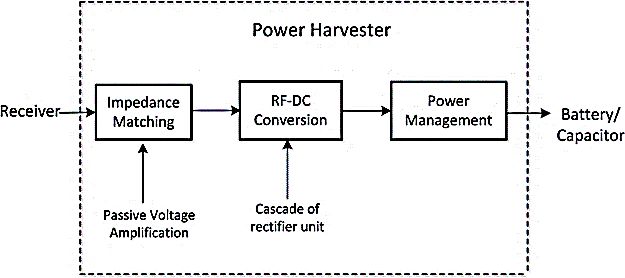
WSEAS TRANSACTIONS on SYSTEMS
DOI: 10.37394/23202.2021.20.27 Chinmoy Bharali, Manash Pratim Sarma
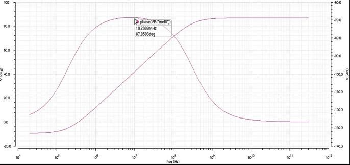
3. 2 Rectifier parameter analysis Figure 8: Magnitude vs Phase plot
As a result, it is observed that the gain of the rectifier
The first parameter that needed to be selected was the device
remains constant after 1 GHz so we choose the operating
length Fig. 5 shows the output voltage variation when the
frequency range for the circuit to be between 200MHz to
transistor length is varied from 65nm to 500nm.
1GHz.
The load resistance of the rectifier is swept from 500 ohms
1,45 to 100K ohms. The graph in the Fig. 9 below shows
different varying parameters of the circuit with variation of
the load resistance.
1,4
Volt(V) 40
1,35 30%)
P.C.E(in
20
1,3 10
0 200 400 600 800 1000
Length(nm) 0 Length(nm)
0 2000
Load Resistance (in4000
ohm) 6000
Figure 5: Simulated output voltage variation versus channel
length
It is observed that after 500nm the output voltage of the
rectifier starts to degrade. The second parameter to be Figure 9: RL vs PCE graph
examined is the transistor width. Fig. 6 shows the alterations
in output voltage when channel width is swept from 65nm to
2000 nm. 1
1,36 0,8
0,6
Pout(mW)
1,35
0,4
Volt(V)
1,34 0,2
1,33 0
0 2000 4000 6000
1,32
Load Resistance (in ohm)
1,31 Figure 10: RL vs Pout graph
0 500 1000 1500 2000 2500
Frequency (Hz)
Fig 10. shows the Load Resistance vs Output Power graph.
Here it is observed that at 1 Kilo ohm load resistor value
Figure 6: Simulated output voltage variation versus channel maximum power is delivered to the load. The calculated
width
input power at this value is 4.09 dBm.
So, it is clear from the graph that after 1000nm the output
voltage of the rectifier starts to degrade. From these two 3.3 MOSFET Output Rise Time
figures the aspect ratio of the devices was chosen.
Initially the operating frequency band of the proposed Turn on time ton= td (on) + tr (Rise time)
design is analyzed in the simulation platform. The RF It is clear from the above equation that if the rise time (t r) of
source frequency here is swept in the RF range 20Khz to the MOSFET is increase then the turn on time of the device
300Ghz. The magnitude and phase plot of the frequency also increases. So, the rise time for the conventional
sweep is given in the Fig. 8 below. Dickson Charge pump is tr= 98.6309607 ns
But, in the proposed circuit the turn on time at 500MHz and
1 GHz operating frequency is 85.055859 ns and 50.10 ns
approx.
Magnitude(dB) The plot for the rise time from 100MHz to 1GHz is shown
in Fig. 11 below
E-ISSN: 2224-2678 246 Volume 20, 2021WSEAS TRANSACTIONS on SYSTEMS
DOI: 10.37394/23202.2021.20.27 Chinmoy Bharali, Manash Pratim Sarma
140
TABLE II.
120
Performance Comparison with other Reported Works
100
Technolo Referen Frequen Input Outpu Loa PCE
80
gy ce cy Power t d (max
60 (dBm) Voltag (K )
40 e ohm
)
20 65 500 -11.39 201.2 10 11.25
0 nm Single mv %
CMOS Stage
0 200 400 600 800 1000 1200
Dickson
180 433 -5 to -9 -- 10 22%
nm Cmos [7] to 30
%
Figure 11: Frequency vs Rise time plot 130 -- -15 1v 100 32%
nm [8] 0
Ou It is observed from the above graph that the rise time keeps CMOS
tp
ut degrading when the Frequency is higher. At 500 MHz the 65 900MHz -18 1v 100 16.8
Ri PCE of the rectifier calculated is 33% at 4dBm input power nm [9] and 0 %
se CMOS 2.4GHz
Ti and at the 1000 MHz the PCE farther degrades to 26% at 45
me 5.7dBm input power. Farther increasing the operating nm This 500MHz 4 916.69 1 33%
(ns
)
frequency, the rise time will certainly fall which is desired CMOS Work 8mv
but at the cost of PCE degradation.
The Optimized parameters of the proposed rectifier is shown in
Table I below.
Frequency (MHz)
TABLE I. Optimized parameters of the proposed rectifier 4. Conclusion
Parameter Optimized Value
MOSFET 45nm The design is implemented using 45nm CMOS process. The
Channel Length threshold compensation is achieved by a scheme that
MOSFET 120nm completely removes the requirement of any other external
Channel Width source and thereby making it fully self-sustainable. The
Operating Frequency 200 MHz to 1 GHz proposed design has attained a PCE of 33% at 4 dBm input
Load Resistance 1kilo ohm power and 26% at 5.7dBm input power at 10K ohm load
PCE 33% (Max) resistance. The design gives a better magnitude gain after 1
M1 Device Turn on voltage -287.12301mV GHz which leads to better sensitivity at low input power
Comparator output current 2.3028 mA (RMS)
levels. The average output voltage at 500MHz input is
Coupling Capacitor (CC) 5pf
916.698mv and at 1GHz the average output voltage is
Output Capacitor (Cout) 70pf
Output Rise time (tr) 85 ns at 500 MHz to 50 ns at
992mv. The aspect ratio of the devices is 3/8. The output
1 GHz rise time is measured to be 85.055859 ns at 500MHz and
50.10 ns at 1GHz. This validates the suitability of the circuit
Hence, it is observed that the threshold voltage to trigger the in RF frequencies with an acceptable PCE and faster
M1 device of the charge pump is lowered from 400mv to - response.
287.1 mV and the turn on period of the device is also
increased.
References.
Table II summarizes the various threshold level
compensated [1] Danial Khan, Seong Jin Oh, Khuram Shehzad, Deeksha
rectifiers parameters for RF energy harvesting. It can be Verma, Young Gun Pu, Minjae Lee, Cheol Hwang,
Youngoo Yang, And Kang-Yoon Lee “An Efficient
seen that our proposed rectifier achieves peak 33% Reconfigurable RF-DC Converter with wide Input
efficiency at 4dBm input power and achieves an output rise Power Range for RF Energy Harvesting” IEEE
time of 85.055859 ns at 500MHz and efficiency of 26% at Access ,Volume: 8, pp- 79310 – 79318, 2020
5.7dBm input power and achieves output rise time of 50ns [2] Mohamed A. Abouzied, Krishnan Ravichandran And
at 1 GHz. Compared to other designs the proposed rectifier Edgar Sánchez-Sinencio Life Fellow, IEEE “A Fully
Integrated Reconfigurable Self-Startup RF Energy-
achieves better efficiency and certainly lowered threshold Harvesting System With Storage Capability” IEEE
value for better switching of MOSFET operating regions. journal of solid-state circuits, Volume: 52, Issue: 3, pp-
704-719,March 2017
[3] Soroush Dehghani, Student member IEEE Shahriar
Mirabbasi And Thomas Johnson, member IEEE “A 5.8-
GHz Bidirectional and Reconfigurable RF Energy
Harvesting Circuit withRectifier and Oscillator Modes”
IEEE Solid-State Circuits Letters Volume: 1, Issue: 3,pp-66-
69, March 2018
E-ISSN: 2224-2678 247 Volume 20, 2021WSEAS TRANSACTIONS on SYSTEMS
DOI: 10.37394/23202.2021.20.27 Chinmoy Bharali, Manash Pratim Sarma
[4] XING LI, CHI-YING TSUI, AND WING-HUNG KI with Hybrid Threshold Voltage Self-Compensation”
“UHF Energy Harvesting System using Reconfigurable Vol. 25, No. 06, 1650055 (2016)
Rectifier for Wireless Sensor Network” IEEE [10] Mansour Taghadosi, Lutfi Albasha , Nasir A. Quadir,
International Symposium on Circuits and Systems Yousuf Abo Rahama, Harshal Chapade, Rajesh Zel
(ISCAS), 2015, Lisbon And Nasser Qaddoumi “High Efficiency Energy
[5] Zizhen Zeng, Xing Li, Amine Bermak, Chi-Ying Tsui Harvesters in 65nm CMOS Process for Autonomous
And Wing-Hung Ki “A Wlan 2.4-GHz RF Energy IoT Sensor Applications” IEEE Access ( Volume: 6),
Harvesting System with Reconfigurable Rectifier for pp- 2397 – 2409, 2017
Wireless Sensor Network” IEEE International [11] Harshal Chapade, Rajesh Zel “On-chip RF to DC
Symposium on Circuits and Systems (ISCAS), 2016, Power Converter for Bio-Medical Application” 32nd
Canada International Conference on VLSI Design and 2019
[6] Zizhen Zeng,, Johan J. Estrada-López, Mohamed 18th International Conference on Embedded Systems
A.Abouzied, And Edgar Sánchez-Sinencio “A (VLSID), 2019, Delhi, India
ReconfigurableRectifier with Optimal Loading Point [12] Mohamed M. Mansour and H. Kanaya . “High-Efficient
Determination for RF Energy Harvesting from -22 dBm Broadband CPW RF Rectifier forWireless Energy
to -2 dBmIEEE Transactions on Circuits and Systems Harvesting” DOI: 10.1109/LMWC.2019.2902461
II: Express Briefs, Volume: 67, Issue: 1, pp-87-91, Jan. [13] Sajjad Shieh and Mahmoud Kamarei,“Transient Input
2020 Impedance Modeling of Rectifiers for RF Energy
[7] S.S. Chouhan and K. Halonen, “Threshold voltage Harvesting Applications” IEEE Transactions on
compensation scheme for RF-to-DC converter used in Circuits and Systems II: Express Briefs, Volume:
RFID applications” DOI:10.1049/el.2015.0445 65, Issue: 3, pp-311-315,March 2018
[8] Z. Hameed and K. Moez, “A 3.2 V –15 dBm Adaptive [14] Ju Ren, Junying Hu, Deyu Zhang, Hui Guo, Yaoxue
Threshold-Voltage Compensated RF Energy Harvester Zhang, and Xuemin (Sherman) Shen “RF Energy
in 130 nm CMOS” IEEE Transactions on Circuits and Harvesting and Transfer in Cognitive Radio Sensor
Systems I: Regular Papers, Volume: 62, Issue: 4, pp- Networks: Opportunities and Challenges” IEEE
948-956, April 2015 Communications Magazine, Volume: 56, Issue: 1, pp-
[9] Lianxi Liu, Wenzhi Yuan , Junchao Mu , Zhu, and 104-110, Jan. 2018
Yintang Yang, “A Dual Band RF Energy Harvester
Creative Commons Attribution License 4.0
(Attribution 4.0 International, CC BY 4.0)
This article is published under the terms of the Creative
Commons Attribution License 4.0
https://creativecommons.org/licenses/by/4.0/deed.en_US
E-ISSN: 2224-2678 248 Volume 20, 2021You can also read