Developing a power supply solution for a mobile robot - Carsten Giesemann, Günter Kemnitz
←
→
Page content transcription
If your browser does not render page correctly, please read the page content below
Developing a power supply solution
for a mobile robot
Carsten Giesemann, Günter Kemnitz

IfI Technical Report Series         IfI-10-03
Impressum

Publisher: Institut für Informatik, Technische Universität Clausthal
     Julius-Albert Str. 4, 38678 Clausthal-Zellerfeld, Germany
Editor of the series: Jürgen Dix
Technical editor: Michael Köster
Contact: michael.koester@tu-clausthal.de
URL: http://www.in.tu-clausthal.de/forschung/technical-reports/
ISSN: 1860-8477

The IfI Review Board

Prof. Dr. Jürgen Dix (Theoretical Computer Science/Computational Intelligence)
Prof. i.R. Dr. Klaus Ecker (Applied Computer Science)
Prof. Dr. Sven Hartmann (Databases and Information Systems)
Prof. i.R. Dr. Gerhard R. Joubert (Practical Computer Science)
apl. Prof. Dr. Günter Kemnitz (Hardware and Robotics)
Prof. i.R. Dr. Ingbert Kupka (Theoretical Computer Science)
Prof. i.R. Dr. Wilfried Lex (Mathematical Foundations of Computer Science)
Prof. Dr. Jörg Müller (Business Information Technology)
Prof. Dr. Niels Pinkwart (Business Information Technology)
Prof. Dr. Andreas Rausch (Software Systems Engineering)
apl. Prof. Dr. Matthias Reuter (Modeling and Simulation)
Prof. Dr. Harald Richter (Technical Informatics and Computer Systems)
Prof. Dr. Gabriel Zachmann (Computer Graphics)
Prof. Dr. Christian Siemers (Embedded Systems)
PD. Dr. habil. Wojciech Jamroga (Theoretical Computer Science)
Dr. Michaela Huhn (Theoretical Foundations of Computer Science)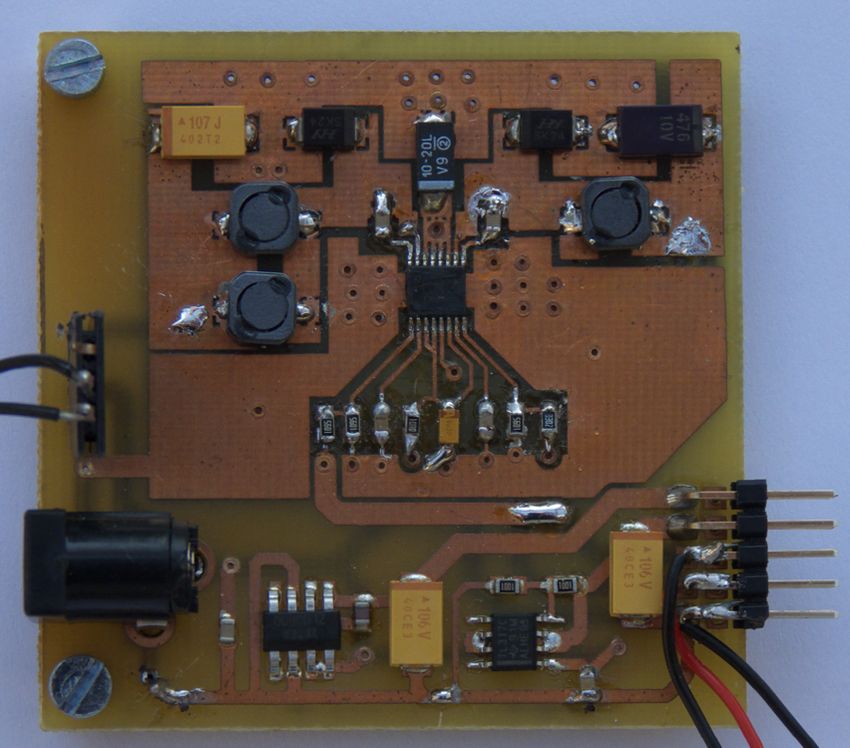
Developing a power supply solution
                    for a mobile robot
                    Carsten Giesemann, Günter Kemnitz

        Department of Informatics, Clausthal University of Technology,
     38678 Clausthal-Zellerfeld, Germany, http://techwww.in.tu-clausthal.de

                                     Abstract
     The article describes the power supply design of a mobile robot. Start-
     ing with the specification of the requirements it describes two prelimi-
     nary designs with an integrated dual-voltage switching power regulator
     circuit, producing disrupted output voltages, and the final successful de-
     sign. The aim of the article is to highlight some aspects of the winding
     way of today’s electronic design processes.

Keywords: power supply, mobile robot, switching power regulator

1    Introduction
For our humanoid robots – type ROBONOVA [3] – extended by a new FPGA
based hardware a new power supply had to be designed. The whole project
is named HuBoTUC (humanoid robots of technical university of clausthal)
[2]. As a suitable Li-Ion accumulator the Samsung L18650 was found having
a capacity of 2700 mAh and a nominal voltage of 3.7 V [5]. The servos have
a supply voltage range from 4.8 V to 6.0 V, so two accumulators have to be
connected in series. The resulting 7.4 V has to be transferred to 6.0 V for the
servos. In addition the FPGA and the rest of the control circuitry need the
following voltages: 5.0 V (≈ 100 mA), 3.3 V (≈ 500 mA), 2.5 V (≈ 10 mA) and
1.2 V (≈ 200 mA). The space for the power supply circuitry is very limited
(only few cm3 ). Wanted operation time is two hours or longer.
   Due to the fact that the 16 servos have a peak current consumption up
to some amperes and the considerable consumption of the 3.3 V voltage,
mainly for the SRAM circuits, no space for cooling devices and the desired
long operation time – fixed voltage regulators are unsuitable. We decided to
use two switched voltage regulators for the high current voltages 6.0 V and
3.3 V and fixed voltage regulators for the rest. After some internet research
the National Semiconductor LM26400Y dual 2 A 500 kHz wide input range

                                         1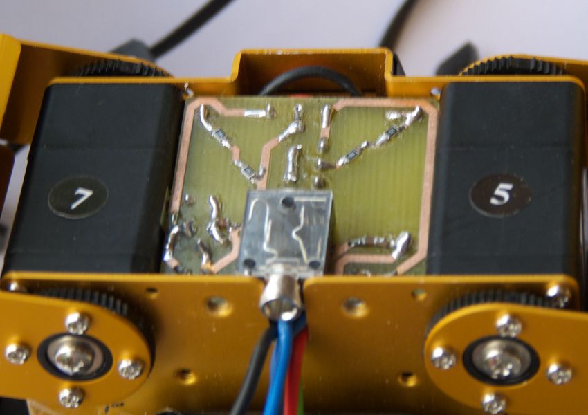
The first design

buck regulator was chosen [6]. It is a very small step-down regulator capable
to provide the two high current voltages. However, after two unsuccessful
attempts a different astonishing simple solution was found and chosen.

2    The first design
Since the robot and its control unit were still under design, the first power
supply has been designed for another FPGA board, needing four off-board
supply voltages: VCCINT (1.2 V), VCCIO (3.3 V), VCCAUX (2.5 V) and 5.0 V.
The switching power regulator has been used for VCCINT (1.2 V) instead of
the 6.0 V, while the VCCIO (3.3 V) remained on the other output. The ad-
ditional voltages had to be generated by some fixed voltage regulators, the
VCCAUX (2.5 V) by a LM317 L from National Semiconductor [7] and the
5.0 V by a ZLDO500, an ultra low dropout fixed voltage regulator from Ze-
tex Semiconductor [4]. The printed circuit board was designed using EAGLE
[1]. Figure 1 shows the circuit diagram from the schematic editor. It is obvi-
ous that the switching power regulator has a more complex circuit than the
fixed voltage power regulators with 2-3 capacitors and – if adjustable – two re-
sistors. All the circuits and the values of the components are taken from the
corresponding datasheets [4, 6, 7]. The PCB (Printed Circuit Board) was self-
manufactured using photo sensitive basis material, chemical etching and
through-plating by rivets. The assembling was also hand-made, using a sol-

                    Figure 1: Schematic of the first design

DEPARTMENT OF INFORMATICS                                                     2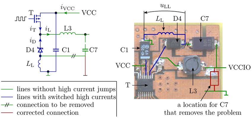
DEVELOPING A POWER SUPPLY SOLUTION FOR A MOBILE ROBOT
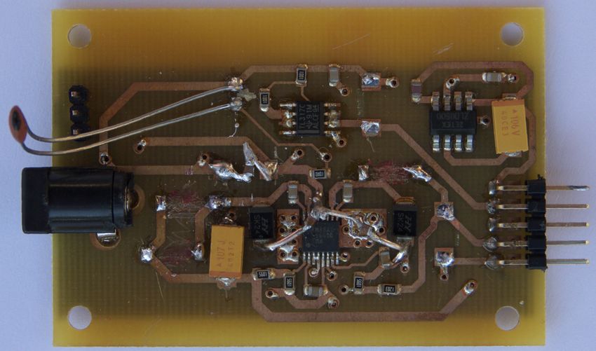
a) b)
Figure 2: a) Board design (the LM26400Y is on the bottom, the LM317LD
and ZLDO500 are on the top) b) Assembled board with additional capacitors,
improved wiring to reduce inductance of critical connections etc.
dering oven for the SMD (Surface-Mounted Device) components (fig. 2).
After the continuity check and the elimination of the shorts and breaks,
the board was put into operation using a laboratory power supply. Both fixed
voltage regulators worked fine and will not receive further consideration.
The LM26400Y produced both of the desired voltages, but with an overlay-
ing disruption, making them unusable. The oscillograph curve showed that
the disruptions were caused by the 500 kHz switching frequency of the reg-
ulator. Deducing from [11], reducing of the inductance of critical wires, in-
creasing the load and/or increasing capacitors could solve the problem. A
load increase had no positive effect. An astonishing side effect was that the
high frequency dirt was even measurable on the ground connection. Addi-
tional 2,2 µF ceramic capacitors close to the regulator reduced the disruption
slightly. Huge electrolytic capacitors around the regulator had no positive
effect, confirming only that the problem cannot be solved in this way. Also
critical wires had been shortened as far as possible (fig. 2 b). Assuming that
the wiring caused the problem, the board was redesigned.
3 The second design
This time the board layout example from the datasheet [6] shown in fig. 3 a
was adapted, having much shorter critical wires but requiring much more
PCB-area. The schematic design remained the same as in fig. 1. The modi-
fied PCB is shown in fig. 3 b and c. This board was also an in-house produc-
tion. After successful continuity check it was put into operation again with
a laboratory power supply.
As in the first design the linear power regulators works flawless and stable
even under high current load. What about the LM26400Y? Little progress
was made. The output voltages are better, but still not clean enough. Trying
3 Technical Report IfI-10-03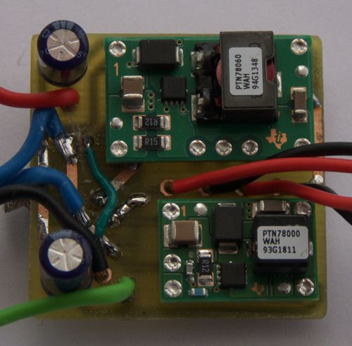
The final design

           a)                          b)                          c)

Figure 3: a) Example layout from the data sheet b) PCB layout c) assembled
board

the same workarounds as before – high load, additional capacitors etc. – the
output voltages did not turn flat. A disappointing result, which leaves two
open questions:

    1. Does the LM26400Y need special components for its circuit?

    2. Are our hand-made and manufactured PCBs the problem?

In the data sheet of the LM26400Y [6] not only the values of the components
are listed but also part numbers of certain component companies. This is a
strong evidence that the first guess is right. On the other hand, our PCBs are
far from being manufactured professionally. For example, rivets for through-
plating were used, which could also cause high frequency problems. Maybe
it is a mixture of both problems. Our simulation und test facilities did not
allow a closer localization.
    How to go on? Engineering is a creative art. Failures are necessary to learn.
It was a »successful failure« like the unsuccessful Apollo 13 mission, were
a technical failure prevented the landing on the moon. The astronauts re-
turned save to earth and the technicians learned how to avoid trouble in fu-
ture. In our case we learned that we cannot handle a high frequency switched
voltage regulator design with our facilities and have to look for a different so-
lution.

4     The final design
As it is often the case, the solution was right in front on the laboratory desk
all the time in form of a Spartan-3A DSP Starter Board, having a similar power
supply as the one to be designed [10]. This board has switched power regu-
lators, however, not assembled of single components, but using two Texas
Instruments PTH switching regulator modules. These modules are available

DEPARTMENT OF INFORMATICS                                                      4
DEVELOPING A POWER SUPPLY SOLUTION FOR A MOBILE ROBOT
Figure 4: Schematic of the final design
for different current ratings, but not for the input voltage of our Li-Ion ac-
cumulator package. Fortunately, there are similar modules with wide input
voltage ranges, named PTN series. Only one resistor is necessary for setting
the output voltage. In addition two capacitors are required – a very simple
solution (fig. 4).
The robot requirements were back in focus. As mentioned earlier, it needs
several voltages. The decision was made to test the 3.0 A module PTN78060W
to produce the 6.0 V servo voltage and the 1.5 A module PTN78000W to pro-
duce the 3.3 V I/O voltage [8, 9]. The other voltages are still produced by
linear power regulators since the loads are small. Of both modules Texas In-
struments send us a free engineering sample, many thanks for it.
a) b)
Figure 5: Final design a) board layout b) assembled board
These modules have the perfect shape to fit into the body of the robot, so
we decided to design the PCB in the right size to find place under the Li-Ion
accumulator. The circuit on the PCB consists beside the voltage modules of
two resistors in a row due to higher precision and two capacitors per module
corresponding to the data sheet. A jack plug for charging the accumulator
and powering the robot from an external source is also added. The on-off
switch will later find its place on the control unit of the robot, so it is only
5 Technical Report IfI-10-03Lessons learned
on flying wires here. All in all the robot control unit and the power supply
unit are connected by five cables. Two cables go to the on-off switch. The
other three are the two power rails and the ground rail (fig. 5). The linear
voltage regulators are on the robot PCB too. Testing showed that all voltages
are clean and stable for the whole load range. After some final adjustments
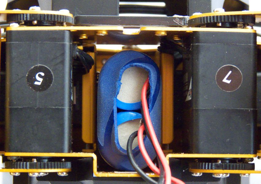
of the layout the boards are finally manufactured and work fine. Figure 6
shows, how the accumulator pack and the designed PCB are mounted within
the robot.
a) b)
Figure 6: Power supply mounted in the robot a ) accumulator double pack b)
PCB covering the accumulator
Figure 7: Circuitry, responsible for the unwanted spikes
5 Lessons learned
Figure 8 shows the waveform of the voltage at the 3.3 V output. There is the
normal small ramping caused by the cyclic increase and decrease of the cur-
DEPARTMENT OF INFORMATICS 6DEVELOPING A POWER SUPPLY SOLUTION FOR A MOBILE ROBOT
Figure 8: The disturbed voltage at the 3.3V output
rent through the inductance superposed by spikes of approximately 500 mV
at the begin of each ramp.
Obviously the switching of the voltage regulator is responsible for the over-
lapping spikes. The part of the circiut diagram with the switched high cur-
rents is shown in fig. 7. It consists of the switching transistor T within the
voltage regulator, the catch diode D4 and the input capacitor C1. The other
currents – the one from the input power supply and the one through the in-
ductance – are without high switched currents so are probably not the cause
of the spikes.
When the transistor switches on, iT approximatly rises from zero to more
then 1 A within few nanoseconds. Simultaniously the current iD reduces to
zero. When the transistor switches off, iT turns to zero causing a jump of
iD by the same amount. The rise or fall of the current is so fast, that over the
small inductances of the wiring with a fast oscilloscope the voltage drops can
be measured, especially over the inductance LL parallel to the catch diode D.
Figure 9 shows the oscillogram.
And then the problem became obviouse. The output capacitor C2 is con-
nected close to the anode of the catch diode, which leads to the circuit dia-
gram in fig. 7 with output capacitor C2 in series with the wiring inductance
LL . Thus the output voltage is superposed by uLL . To check the assumption
7 Technical Report IfI-10-03References
Figure 9: The voltage uLL
we rearranged the output capacitor as indicated in fig. 7. As shown in fig. 10,
the rearrangement of the capacitor almost solved the problem.
6 Conclusions
Electronic design has its own philosophy. In contrast to software one can-
not simply design a circuit from components that works at once, especially
a high frequency analog circuit. Sometimes, it is better to abandon an own
solution and look for alternatives. Maybe it is – as here – right on the desk
and needs only to be discovered.
References
[1] EAGLE website. http://www.cadsoft.de/.
[2] HuBoTUC website.
http://techwww.in.tu-clausthal.de/site/Projekte/HuBoTUC/.
[3] Robonova website. http://www.robonova.com/.
DEPARTMENT OF INFORMATICS 8DEVELOPING A POWER SUPPLY SOLUTION FOR A MOBILE ROBOT
Figure 10: The voltage after rearranging C2 measured over C2
[4] ZLDO500 5.0 volt ultra low dropout regulator.
http://www.diodes.com/, 1997.
[5] L18650 data sheet. http://www2.produktinfo.conrad.com/datenblaetter/
250000-274999/251024-da-01-en-LI_ION_Akku_Samsung_L18650.pdf,
2006.
[6] LM26400Y Dual 2A, 500kHz Wide Input Range Buck Regulator.
http://www.national.com/, 2007.
[7] LM317L 3-Terminal Adjustable Regulator. http://www.national.com/,
2008.
[8] PTN78000W, PTN78000H 1.5-A, wide-input adjustable switching regu-
lator. http://www.ti.com/, 2008.
[9] PTN78060W, PTN78060H 3-A, wide-input adjustable switching regula-
tor. http://www.ti.com/, 2009.
[10] Spartan-3A DSP Starter, Platform User Guide. http://www.xilinx.com/,
2009.
[11] Günter Kemnitz. Technische Informatik 1: Elektronik. Springer, 2010.
9 Technical Report IfI-10-03You can also read