A Simple Method to Control the Growth of Copper Oxide Nanowires for Solar Cells and Catalytic Applications
←
→
Page content transcription
If your browser does not render page correctly, please read the page content below
Hindawi
Advances in Condensed Matter Physics
Volume 2020, Article ID 5470817, 8 pages
https://doi.org/10.1155/2020/5470817

Research Article
A Simple Method to Control the Growth of Copper Oxide
Nanowires for Solar Cells and Catalytic Applications

 L. Nkhaili , A. Narjis, A. Agdad, A. Tchenka, A. El Kissani, A. Outzourhit, and A. Oueriagli
 Nanomaterials for Energy and Environment Laboratory, Physics Department, Faculty of Sciences Semlalia,
 Cadi Ayyad University, P.O. Box 2390, Marrakech 40000, Morocco

 Correspondence should be addressed to L. Nkhaili; lahcen.com@hotmail.fr

 Received 14 April 2020; Revised 23 July 2020; Accepted 1 September 2020; Published 12 September 2020

 Academic Editor: Charles Rosenblatt

 Copyright © 2020 L. Nkhaili et al. This is an open access article distributed under the Creative Commons Attribution License,
 which permits unrestricted use, distribution, and reproduction in any medium, provided the original work is properly cited.
 Copper oxide nanowires (CuO NWs) were synthesized by thermally oxidizing copper foils at various heating rates. It has been
 shown that both monoclinic CuO and cubic Cu2O phases were grown on the copper surface with NW diameters of almost 200 nm
 for all samples. While NWs were shown to be dense for low heating rates, they end up being broken for quick heating. The
 underlying growth mechanism was described basing on a detailed comprehensive study, and the effect of the heating rate was
 explained by considering the thermal shock effect and in-plane tensile stresses on curved surfaces. This study contributes to the
 research for suitable methods for the use of recyclable metals in technological applications. In particular, copper oxide NWs were
 deposited, for the first time, on FTO/glass substrates, and the optical characterization revealed that this method is a promising way
 to improve the surface contact for solar cells and catalytic applications.

1. Introduction CuO NWs can be synthesized by several methods [18],
 including chemical routes [19–22], direct plasma oxidation
Cupric oxide (CuO) and cuprous oxide (Cu2O) are p-type [23, 24], and thermal oxidation of copper substrates
semiconductors with a band gap of 1.2 and 2 eV, respec- [10–15, 25]. The latter is a pragmatic method.
tively. Their electrical and optical properties make them very
useful as interesting constituents in photovoltaic applica-
tions [1–3], gas and liquid sensors [4, 5], electron stable
 2. Thermal Oxidation of Copper Substrates
source in optoelectronic devices [6, 7], and organic catalysts Heating directly leads to synthesize copper oxide NWs on
[8, 9]. the surface of a copper substrate, either as a foil [10–15], a
 CuO nanowires (NWs) have been intensively synthe- wire [10], a grid [10], a thin film [25], or nanoparticles [26].
sized and studied over the course of the last few years This method is carried out at high temperature, typically
[10–15]. Their large surface area makes them very interesting between 400°C and 700°C, in air or in other static or flowing
for the abovementioned applications. In fact, the large atmosphere (pure O2, a mixture of O2 and Ar gases, and so
surface contact in a p-n junction leads to a significant on).
generation of excitons, which enhances the photocurrent in The pioneer synthesis of CuO NWs by the thermal
the solar cell and partially overcomes the phenomenon of oxidation method was performed by Jiang et al. on different
recombination due to the limited scattering length of substrates during 4 hours [10]. The observed length was up
electron-hole pairs near the depletion region. Similarly, the to 15 μm, and the NW diameter was found to be 100, 50, and
gas sensing gets favored on NWs because of the large surface 30 nm for the heating temperature of 400, 500, and 600°C,
area [16, 17]. The sharp tips of the CuO NWs lead to a large respectively. Later, Xu et al. also synthesized CuO NWs by
electrical field at its boundaries. This justifies its uses as an heating copper foils [11]. Their results concerning the length
electron source in optoelectronic devices. and the diameters were comparable to that found by Jiang
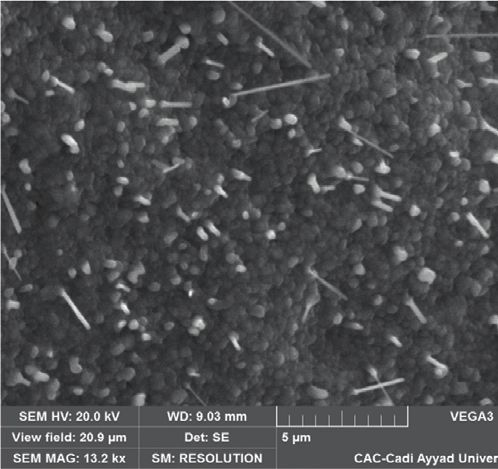
2 Advances in Condensed Matter Physics

et al. [10] with remarkably high NWs density for the heating NWs needs to use a slow heating. To further confirm this
temperature of 500 and 600°C. assumption, another copper substrate was heated at the rate
 The morphological properties of CuO NWs (diameter, of 15°C/min. The SEM image of the so obtained sample is
length, density) have been shown to depend on the heating shown in Figure 2-right. By quick heating, the NWs were
temperature [27, 28], the treatment time [28], and the destructed. In fact, some of them were displayed with a
substrate nature [10]. However, to the best of our knowledge, noteworthy fragility. To explain the effect of the heating rate
no study has been devoted to the heating rate effect. on the CuO NWs growth, a comprehensive study on the
 In this paper, CuO NWs have been synthesized by underlying mechanism was required.
thermal oxidation at 550°C for 4 hours in air. The effect of the Two mechanisms have been commonly described to
heating rate was studied down to 1°C/min. Physical expla- explain the growth of NWs in the gas phase: Vapor-Liquid-
nations are given based on the underlying growth mecha- Solid (VLS) [29] and Vapor-Solid (VS) [30]. The VLS is
nism. As application, CuO NWs were deposited on a copper excluded because no NW was terminated by spherical
thin film for using in solar cells and catalytic applications. particle, and the VS mechanism is also excluded for two
 reasons: First, no CuO was observed to depose around the
3. Experimental sample, and second, the growth of CuO NWs occurs at a
 temperature much lower than the melting points (1232°C for
Each recyclable copper foil (intended for public uses) is with Cu2O and 1326°C for CuO). In a previous study, the vapor
a thickness of 0.3 mm. It was ultrasonically cleaned for pressure of CuO has been observed to be just
10 min in ethanol, 10 min in acetone, and 10 min in distilled 1.15 × 10⁻⁴ mm·Hg at 800°C [31, 32].
water and, then, heated in air using a Nabertherm box The most probable mechanism is the stress-induced
furnace for 4 hours. Copper oxide NWs could be grown by diffusion. This process has been previously supported by
heating at a temperature between 400 and 700°C [10, 11]. In experimental observations [33, 34] and explained by Li et al.
the present investigation, all substrates were heated at 550°C. [35] as follows: (a) formation of monoclinic crystal nuclei
However, the heating rate took various values. with a pointed rhombic prism shape and (b) growth of CuO
 As applications, CuO NWs were deposited on a copper NWs on a continuous CuO scale because of the short-circuit
thin film. The latter was prepared by the electrodeposition diffusion of copper ions trough grain surfaces. This expla-
method on an FTO-coated glass substrate using standard nation was also supported by the experimental data, and it
three electrodes. We used an FTO substrate of 0.8 × 1.5 cm as used the theory of crystallography (TOC) [36]. However, the
a working electrode (WE), a platinum mesh was used as a starting reactive was Cu2O instead of copper. In the present
counter electrode (CE), and a saturated calomel electrode case, the stress-induced diffusion of Cu2+ ions is believed to
(SCE) as a reference electrode. The thin films were deposited be valid, including the thermal and compressive stresses. The
from an aqueous solution containing 0.4 M copper sulphate growth of CuO NWs on a copper substrate can be described
(CuSO4·5H2O) and 3 M lactic acid. The pH of the bath by considering the following process. At the beginning,
solution was adjusted to 5 by sodium hydroxide (NaOH) copper is oxidized following the reaction
maintained at 60°C, and Cu films were deposited within the
potentiostatic mode by imposing a voltage of V � 0.4 V/SCE 1
 2Cu + O2 ⇄ Cu2 O (1)
during 800 s. The thickness of the Cu thin film is 0.6 μm 2
measured using the Michelson interferometer. NWs grown During the next step, Cu2O served as a precursor to
on Cu films on FTO were synthesized by thermal oxidation CuO. Indeed, the chemisorbed oxygen attracts an electron
at 500°C for 4 hours in air at a step of 2°C/min. from the Cu2O lattice, and then, fully ionized oxygen reacts
 X-Ray Diffractions (DRX) were performed using a with a Cu2+ ion according the reaction:
Bruker D8 Advanced Diffractometer. Scanning electron
microscopy and energy dispersive X-ray microanalysis were 1 2−
 O ⇄ CuO + 2h+ + VCu (2)
carried out on a VEGA3 TESCAN. Optical transmittance 2 2
data were taken using a Shimadzu UV-PC spectropho-
 The emerging holes (2h+) and copper ion vacancy
tometer in the 200–3200 nm range.
 (having a positive charge of +2e and a negative charge of −2e,
 respectively) are attracted by a molecular Cu2O to form a
4. Results and Discussion CuO molecule as follows:
 2−
For the heating rates of 1, 2, 5, and 10°C/min, representative Cu2 O + 2h+ + VCu ⇄ CuO (3)
SEM images of the obtained samples are displayed in Fig-
ure 1. All surfaces were covered by NWs with comparable We believe that both the Cu2O cubic lattice and CuO
diameter, which is found to be almost 200 nm. Also, we monoclinic lattice coexist in the thin film. This was con-
noticed that the NWs’ density is stable and, then, decreases firmed by performing the XRD displayed in Figure 3. The
by increasing the heating rate (Table 1). However, some reaction (3) is known to be very slow. However, it results in a
regions exhibit less dense NWs islands. Figure 2-left shows significant effect on the final composition and shape of the
this observation for the heating rate of 5°C/min using an- oxide. Indeed, the precipitation of monoclinic crystal nuclei
other scale. The uncovered surface was found to increase exhibits pointed ends in the critical nucleus according to the
with increasing heating rate. Thus, the formation of dense TOC [36]. As the electric field is strong at the points, charges
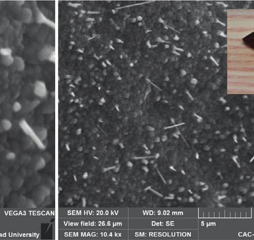
Advances in Condensed Matter Physics 3

 (a) (b)

 (c) (d)

Figure 1: SEM images for CuO NWs obtained by thermal oxidation of copper foils at 550°C for 4 h The heating rates are (a) 1°C/min; (b)
2°C/min; (c) 5°C/min; and (d) 10°C/min. While the diameter is almost the same in all samples, the NW density slightly decreases with
increasing the heating rate.

Table 1: NWs density estimated by the SEM images and crystallite size calculated using the Scherrer equation for various heating rates.
 Crystallite size (nm)
Heating rate (°C/min) NWs density (×108 cm−2)
 CuO Cu2O
1 2.8 24.9 20
2 2.2 25.9 24.8
5 2.9 25.9 24.8
10 1.1 24.8 23

 a
 c
 b

Figure 2: SEM images for the sample synthesized at 5°C/min (left)- a: dilute island; b: NWs finished being broken; and c: dense island; the
sample synthesized at 15°C/min (right). The lack of homogeneity and the NWs breaking are caused by the thermal shock-induced in-plane
tensile stresses.
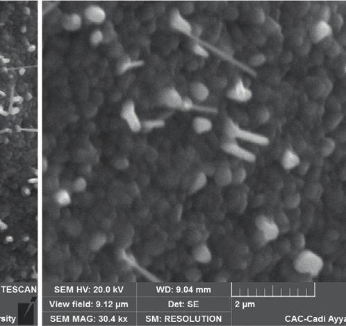
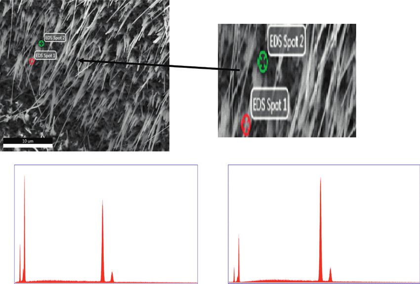
4 Advances in Condensed Matter Physics

 increases with decreasing EN. On the other hand, ΔGV < 0,
 ΔGs > 0, and |ΔGs | < |ΔGV |, so that the decrease of ΔGs re-
 sults in increasing the denominator of equation (4). This
 + 10°C/min results in decreasing EN. Hence, one method to enhance the
 NWs density is to reduce ΔGs. This can be achieved by
 exerting bending stresses on the copper surface [38].
 Intensity (a.u)

 5°C/min However, some regions of the treated samples were naturally
 bent (in the initial form or by thermal shock during heating).
 This explains the appearance of dense and dilute NWs is-
 2°C/min
 lands. The underlying mechanism is shown in Figure 5. By
 heating a bent substrate, the in-plane tensile stresses result in
 the reduction of the lattice mismatch between the copper
 1°C/min and the oxide lattices (ΔGs decreases) and the NWs density is
 0
 expected to increase. In our case, however, some NWs are
 20 30 40 50 60 70 broken because of the small base, which reduces the NWs
 2θ (°) density. It is worth noticing that the region b in Figure 5
 shows compressive stresses. However, this does not result in
 CuO
 any change in the NWs density as compared with the unbent
 Cu2O
 region [38].
Figure 3: XRD pattern of the four samples obtained by the heating In the present study, some regions were naturally bent
rates 1, 2, 5, and 10°C/min. Both copper oxides have been observed and the in-plane tensile stresses make them covered by dense
to appear by thermal oxidation of copper foils at 550°C for 4 h. NWs. On the contrary, NWs are less dense on the unbent
 regions. For the sample heated at a rate of 15°C/min, quick
are easily attracted to form an accumulating CuO layers on heating enhances curvature of some bent regions. The in-
the NW tip. plane tensile stresses result in small oxide grain size and,
 It is worth noticing that the amount of the Cu2O phase therefore, lead to form small nucleation sites, NWs on which
decreases by decreasing the heating rate since the reaction 3 end up being broken. Hence, the grain size was expected to
took its enough time to take place. Indeed, the corre- be small for slow heating. To confirm this assumption, NWs
sponding peaks in the XRD pattern are not as intense as formed by the heating at 2°C/min were cleaned by acetone to
those of the CuO phase for the heating rate of 1°C/min. On show its nucleation sites by the SEM (Figure 6(a)). Com-
the other hand, the crystallite sizes calculated using the pared with the nucleation sites of the sample synthesized at
Scherrer equation did not exhibit a significant change by 15°C/min (Figure 6(b)), nucleation sites at slow heating are
varying the heating rate (Table 1). more compact with lower porosity.
 Given the abovementioned explanations, each NW was
expected to be formed of monoclinic CuO lattices and its
nucleation site may contain Cu2O cubic lattices. In fact, the 5. Application: Synthesis of CuO NWs on FTO/
EDX microanalysis performed on the sample synthesized at Glass Substrates
10°C/min showed that copper and oxygen percentages are
 As application, we deposited CuO NWs on copper thin films
almost equal on the NW (spot 1 in Figure 4) indicating that
 deposited by the electrodeposition method on an FTO-
the NW is formed by the CuO lattice, whereas on the NW
 coated glass substrate. The underlying aim is to obtain
base, the percentage of copper was shown to be more than
 transparent films for using in solar cells and catalytic ap-
two times greater than that of oxygen (spot 2 in Figure 4),
 plications. In fact, by obtaining NWs array, the surface
which may be due to the existence of CuO, Cu2O, and Cu
 contact at the solar cell junction or between the reactors and
lattices on the NW base.
 the catalyst (thin film) increases, and thus, the efficiency is
 To obtain NWs with high density, intense outward
 expected to increase in both cases.
diffusions are required. Therefore, continuous supply of
 As shown in Figure 7(a), the obtained phase is for copper
copper ions through grain boundaries has to be ensured. The
 oxide. On the other hand, the SEM images (Figure 7(c))
nucleation of NWs islands is obtained when the underlying
 show that CuO NWs were obtained on the deposited copper
layer is enough dense to overcome the nucleation barrier. By
 film. The EDX analysis (Figure 7(d)) revealed that the ox-
considering heterogeneous nucleation of an oxide island on
 ygen percentage is 55.4%, while that of copper is 41.8%,
the metal surface, this barrier is written as [37]
 which corresponds to the CuO compound. The transmission
 1 spectra of the films are depicted in Figure 7(b). Average
 EN � f(θ)σ 3 2, (4)
 ΔGs + ΔGV transmittance in the visible spectrum was lower than 1%
 with the band gap (Eg) values calculated from the extrap-
where f(θ) is a geometric function. σ is the surface energy of olation of linear line portion of the plot of (αh])2 versus (h])
the oxide, ΔGs is the energy due to the lattice mismatch as shown in the Figure 7(b). The band gap value of CuO
between the copper and its oxide, and ΔGV is the free energy nanowires was found to be about 1.21 eV. The absorption
of the oxidation reaction. The number of nucleation sites coefficient (α) is calculated using the following relation:
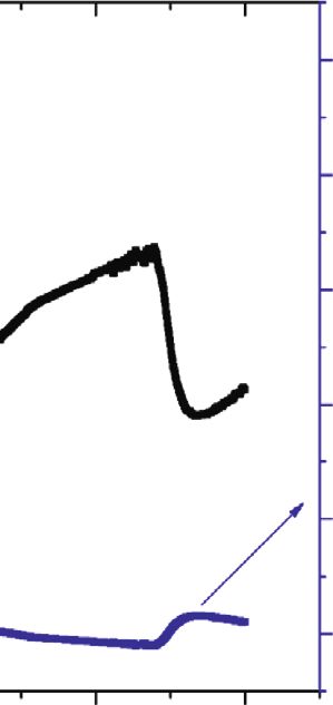
Advances in Condensed Matter Physics 5

 1.70K
 Cu 1.26 K
 1.53K O: 46.2% O: 18.2%
 1.36K 1.12 K
 Cu 0.98 K Cu: 81.8%
 1.19K Cu: 53.8%
 1.02K 0.84 K
 0.85K 0.70 K Spot 2
 Spot 1 Cu
 0.68K 0.56 K
 0.51K 0.42 K
 0.34K 0.28 K O Cu
 0.17K Cu 0.14 K
 0.00K 0.00 K
 0.0

 1.7

 3.4

 5.1

 6.8

 8.5

 10.2

 11.9

 13.6

 15.3
 0.0

 1.7

 3.4

 5.1

 6.8

 8.5

 10.2

 11.9

 13.6

 15.3

 Lsec: 29.90 Cnts 0.000 keV Det: Octane plus det Lsec: 30.00 Cnts 0.000 keV Det: Octane plus det

Figure 4: EDX analysis for the sample obtained by heating at 10°C/min. Spot 1: the NW contains the CuO lattice. Spot 2: the nucleation site
base may contain CuO, Cu2O, and Cu lattices.

 a b c

Figure 5: Effect of the bending stresses on the NWs density. Arrows indicate the corresponding stresses. In-plan tensile stresses on the top
surface of the bent region (region a) result in the growth of dense NWs. On the contrary, the unbent region (region c) is covered by less dense
NWs because of the grain size.

 (a) (b)

Figure 6: SEM image of nucleation sites for the samples synthesized at (a) 2°C/min after cleaning NWs by acetone and (b) 15°C/min. The
slow heating results in more compact nucleation sites with low porosity.
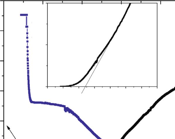
6 Advances in Condensed Matter Physics

 30

 (αhν)2 (ev2cm–2)
 25
 –

 Transmittance (%)
 20 Eg = 1.21eV

 Absorbance (a.u)
 Intensity (a.u)

 +
 15

 0.0
 0.5
 1.0
 1.5
 2.0
 2.5
 3.0
 3.5
 hν (eV)
 10
 – –
 ∗ + –
 – +
 + – 5
 ∗ ∗ ∗∗ ∗
 + –
 0
 20 30 40 50 60 70 0 500 1000 1500 2000 2500 3000
 2θ Wavelength (nm)
 – CuO
 + Cu2O
 ∗ FTO
 (a) (b)

 (c)

 225
 200
 175
 150
 125
 100
 75
 50
 25
 0
 0.00 0.57 1.34 2.01 2.58 3.35 4.00 4.59 5.36 6.23

 Element Weight (%) Atomic (%) Net int. Error (%)
 O 22.90 55.43 14.68 18.57
 Cu 68.53 41.77 22.83 17.55
 Sn 8.57 2.79 1.09 61.71
 (d)

Figure 7: Data for the CuO NWs deposited on a thin copper film. (a) XRD patterns, (b) transmittance and absorbance data, (c) SEM images
with a photo of a sample in the inset, and (d) EDX analysis for the sample obtained on the thin copper film.

 ln(1/T) Figure 7(b). It is noted that the synthesized NWs exhibit a
 α� , (5) high absorbance, which indicates that the synthesized
 d
 compound is a good candidate for solar cells and catalytic
where α is the absorption coefficient, T is the transmittance, applications, and this high absorption is one of the prop-
and d is the film’s thickness. The absorption was slightly erties that explain the interest in thin films in the field of
better for the film, and prepared data are shown in photovoltaic conversion.
Advances in Condensed Matter Physics 7

6. Conclusions discussed the obtained results. He contributed to analysing
 and writing the paper.
For involvement in solar cells and catalytic activities ap-
plications, copper oxide NWs have been successfully syn-
thesized by thermal oxidation of copper foils. Experimental Acknowledgments
data showed that the Vapor-Solid mechanism and the The authors are grateful to Prof. Said Laasri from the Na-
Vapor-Liquid-Solid mechanism are excluded, and the CuO tional School of Applied Sciences of El jadida, Morocco, who
nucleation was found to show a diffusion-controlled be- helped to perform the XRD. A.N thanks Dr. Lahoucine
havior. The formation of the CuO monoclinic phase leads to Atourki from Ibn Zohr University, Morocco, for his help.
a pointed rhombic prism base for NWs nucleation.
 Local bending is enhanced by thermal shock, which
increases by increasing the heating rate and results in an References
increasing in the in-plane tensile stresses, which reduces the
 [1] M. Izaki, T. Shinagawa, K.-T. Mizuno, Y. Ida, M. Inaba, and
size of nucleation sites, and, hereby, enhances the NWs A. Tasaka, “Electrochemically constructed p-Cu2O/n-ZnO
density. However, thick sites are needed to have rigid NWs heterojunction diode for photovoltaic device,” Journal of
and avoid their breaking. This study may have a broader Physics D: Applied Physics, vol. 40, no. 11, p. 3326, 2007.
impact for using recyclable metals in some technological [2] S. Ishizuka, K. Suzuki, Y. Okamoto et al., “Polycrystalline n-
devices. ZnO/p-Cu2O heterojunctions grown by RF-magnetron
 As application, CuO NWs were successfully deposited sputtering,” Physica Status Solidi (C), vol. 1, no. 4, p. 1067,
on a copper thin film electrodeposited on an FTO/glass 2004.
substrate. Structural and optical characterizations revealed [3] J. Katayama, K. Ito, M. Matsuoka, and J. Tamaki, “Perfor-
that the thermal oxidation is a suitable way to obtain a large mance of Cu2O/ZnO solar cell prepared by two-step elec-
contact surface and, consequently, improve the efficiency of trodeposition,” Journal of Applied Electrochemistry, vol. 34,
 no. 7, p. 687, 2004.
the device.
 [4] N. D. Hoa, N. van Quy, H. Jung, D. Kim, H. Kim, and
 S.-K. Hong, “Synthesis of porous CuO nanowires and its
Data Availability application to hydrogen detection,” Sensors and Actuators B:
 Chemical, vol. 146, no. 1, p. 266, 2010.
The characterization data and experimental results used to [5] D. Li, J. Hu, R. Wu, and J. G. Lu, “Conductometric chemical
support the findings of this study are included within the sensor based on individual CuO nanowires,” Nanotechnology,
article. vol. 21, no. 48, p. 485502, 2010.
 [6] Z. Chen, T. F. Jaramillo, T. G. Deutsch et al., “Accelerating
Disclosure materials development for photoelectrochemical hydrogen
 production: standards for methods, definitions, and reporting
A part of this paper was used for participation in the Fifth protocols,” Journal of Materials Research, vol. 25, no. 1, p. 3,
International Symposium on Dielectric Materials and Ap- 2010.
plications ISyDMA’5 (see the link “https://www.isydma. [7] D. Mariotti and R. M. Sankaran, “Microplasmas for nano-
com/poster-session-iii-2/”). materials synthesis,” Journal of Physics D: Applied Physics,
 vol. 43, no. 32, Article ID 323001, 2010.
 [8] A. Angi, D. Sanli, C. Erkey, and O. Birer, “Catalytic activity of
Conflicts of Interest copper (II) oxide prepared via ultrasound assisted Fenton-like
The authors declare that there are no conflicts of interest reaction,” Ultrasonics Sonochemistry, vol. 21, p. 854, 2014.
 [9] T. Ben-Moshe, I. Dror, and B. Berkowitz, “Oxidation of or-
regarding the publication of this paper.
 ganic pollutants in aqueous solutions by nanosized copper
 oxide catalysts,” Applied Catalysis B: Environmental, vol. 85,
Authors’ Contributions no. 3-4, pp. 207–211, 2009.
 [10] X. Jiang, T. Herricks, and Y. Xia, “CuO nanowires can Be
L. Nkhaili is the first author. He contributed to all experi- synthesized by heating copper substrates in air,” Nano Letters,
ments and a big part of the redaction. A. Narjis contributed vol. 2, no. 12, p. 1333, 2002.
to preparing samples, performing the SEM images, and in [11] C. H. Xu, C. H. Woo, and S. Q. Shi, “Formation of CuO
analysing the NWs growth mechanism. He contributed in all nanowires on Cu foil,” Chemical Physics Letters, vol. 399,
works of the paper. A. Agdad contributed to the discussion no. 1–3, p. 62, 2004.
of a part of the X-ray Diffractions (DRX) patterns. He [12] J. T. Chen, F. Zhang, J. Wang et al., “CuO nanowires syn-
contributed to experimental detail and the results and thesized by thermal oxidation route,” Journal of Alloys and
discussion. A. Tchenka contributed to preparing samples Compounds, vol. 454, no. 1-2, p. 268, 2008.
and analysing optical data. A. El kissani contributed to [13] Y.-S. Kim, I.-S. Hwang, S.-J. Kim, C.-Y. Lee, and J.-H. Lee,
 “CuO nanowire gas sensors for air quality control in auto-
preparing samples and analysing optical data. He contrib-
 motive cabin,” Sensors and Actuators B: Chemical, vol. 135,
uted to experimental detail and the results and discussion. no. 1, p. 298, 2008.
A. Outzourhit contributed to the improvement of the En- [14] W. Wang, Y. Zhan, and G. Wang, “One-step, solid-state
glish of the manuscript. He supervised all our works, in- reaction to the synthesis of copper oxide nanorods in the
cluding this paper. A. Oueriagli helped to access the presence of a suitable surfactant,” Chemical Communications,
experiences and the necessary measurements. Also, he vol. 8, no. 8, pp. 727-728, 2001.
8 Advances in Condensed Matter Physics

[15] N. Mukherjee, A. Mondal, and U. Madhu, “Chemical bath of YBaCuO thin films,” Superconductor Science and Tech-
 deposition of thin films of CuO nanorods and their charac- nology, vol. 5, no. 11, p. 624, 1992.
 terisation,” International Journal of Nanomanufacturing, [33] L. Yuan, Y. Wang, R. Mema, and G. Zhou, “Driving force and
 vol. 5, no. 1/2, p. 16, 2010. growth mechanism for spontaneous oxide nanowire forma-
[16] U. Cvelbar, K. Ostrikov, A. Drenik, and M. Mozetic, tion during the thermal oxidation of metals,” Acta Materialia,
 “Nanowire sensor response to reactive gas environment,” vol. 59, no. 6, p. 2491, 2011.
 Applied Physics Letters, vol. 92, no. 13, p. 133505, 2008. [34] M. Chen, Y. Yue, and Y. Ju, “Growth of metal and metal oxide
[17] M. Meyyappan, “Catalyzed chemical vapor deposition of one- nanowires driven by the stress-induced migration,” Journal of
 dimensional nanostructures and their applications,” Progress Applied Physics, vol. 111, no. 10, p. 104305, 2012.
 in Crystal Growth and Characterization of Materials, vol. 55, [35] A. Li, H. Song, J. Zhou, X. Chen, and S. Liu, “CuO nanowire
 no. 1-2, p. 1, 2009. growth on Cu2O by in situ thermal oxidation in air,” Crys-
[18] G. Filipic and U. Cvelbar, “Copper oxide nanowires: a review tEngComm, vol. 15, no. 42, p. 8559, 2013.
 of growth,” Nanootechnology, vol. 23, no. 19, p. 194001, 2012. [36] S. Q. Zhao, Crystallography and Mineralogy, Higher Educa-
[19] Y.-H. Lee, I.-C. Leu, M.-T. Wu, J.-H. Yen, and K.-Z. Fung, tion Press, Beijing, China, 2005.
 “Fabrication of Cu/Cu2O composite nanowire arrays on Si via [37] G. Zhou, “Nucleation thermodynamics of oxide during metal
 AAO template-mediated electrodeposition,” Journal of Alloys oxidation,” Applied Physics Letters, vol. 94, no. 20, p. 201905,
 and Compounds, vol. 427, no. 1-2, p. 213, 2007. 2009.
[20] B. S. Khan, A. Saeed, S. S. Hayat, A. Mukhtar, and [38] R. Mema, L. Yuan, Q. Du, Y. Wang, and G. Zhou, “Effect of
 T. Mehmood, “Mechanism for the formation of cuprous oxide surface stresses on CuO nanowire growth in the thermal
 nanowires in AAO template by electrodeposition,” Interna- oxidation of copper,” Chemical Physics Letters, vol. 512,
 tional Journal of Electrochemical Science, vol. 12, pp. 890–897, no. 1–3, pp. 87–91, 2011.
 2017.
[21] W. Wang, Y. Zhuang, and L. Li, “Structure and size effect of
 CuO nanowires prepared by low temperature solid-phase
 process,” Materials Letters, vol. 62, no. 10-11, p. 1724, 2008.
[22] W. Z. Wang, G. H. Wang, X. S. Wang, Y. J. Zhan, Y. K. Liu,
 and C. L. Zheng, “Synthesis and characterization of Cu2O
 nanowires by a novel reduction route,” Advanced Materials,
 vol. 14, no. 1, p. 67, 2002.
[23] G. Arnoult, R. P. Cardoso, T. Belmonte, and G. Henrion,
 “Flow transition in a small scale microwave plasma jet at
 atmospheric pressure,” Applied Physics Letters, vol. 93, no. 19,
 p. 191507, 2008.
[24] V. Kumar, J. H. Kim, J. B. Jasinski, E. L. Clark, and
 M. K. Sunkara, “Alkali-assisted, atmospheric plasma pro-
 duction of titania nanowire powders and arrays,” Crystal
 Growth & Design, vol. 11, no. 7, p. 2913, 2011.
[25] S. Wang, Q. Huang, X. Wen, X.-y. Li, and S. Yang, “Thermal
 oxidation of Cu2S nanowires: a template method for the
 fabrication of mesoscopic CuxO (x � 1, 2) wires,” Physical
 Chemistry Chemical Physics, vol. 4, no. 14, p. 3425, 2002.
[26] C.-T. Hsieh, J.-M. Chen, H.-H. Lin, and H.-C. Shih, “Synthesis
 of well-ordered CuO nanofibers by a self-catalytic growth
 mechanism,” Applied Physics Letters, vol. 82, no. 19, p. 3316,
 2003.
[27] J. Liang, N. Kishi, T. Soga, and T. Jimbo, “Cross-sectional
 characterization of cupric oxide nanowires grown by thermal
 oxidation of copper foils,” Applied Surface Science, vol. 257,
 no. 1, pp. 62–66, 2010.
[28] A. M. B. Goncalves, L. C. Campos, A. S. Ferlauto, and
 R. G. Lacerda, “On the growth and electrical characterization
 of CuO nanowires by thermal oxidation,” Journal of Applied
 Physics, vol. 106, Article ID 034303, 2009.
[29] R. S. Wagner and W. C. Ellis, “Vapor-liquid-solid mechanism
 of single crystal growth,” Applied Physics Letters, vol. 4, no. 5,
 p. 89, 1964.
[30] S. S. Brenner and G. W. Sears, “Mechanism of whisker
 growth-III nature of growth sites,” Acta Metallurgica, vol. 4,
 no. 3, p. 268, 1956.
[31] E. Mack, G. G. Osterhof, and H. M. Kraner, “Vapor pressure
 of copper oxide and of copper,” Journal of the American
 Chemical Society, vol. 45, p. 617, 1923.
[32] H. Busch, A. Fink, A. Muller, and K. Samwer, “Occurrence
 and origin of copper oxide particulates prior to the deposition
You can also read