A Terahertz Molecular Clock on CMOS Using High-Harmonic-Order Interrogation of Rotational Transition for Medium-/Long-Term Stability Enhancement ...
←
→
Page content transcription
If your browser does not render page correctly, please read the page content below
566                                                                               IEEE JOURNAL OF SOLID-STATE CIRCUITS, VOL. 56, NO. 2, FEBRUARY 2021

       A Terahertz Molecular Clock on CMOS Using
      High-Harmonic-Order Interrogation of Rotational
            Transition for Medium-/Long-Term
                   Stability Enhancement
                               Cheng Wang , Member, IEEE, Xiang Yi , Senior Member, IEEE,
                                Mina Kim , Graduate Student Member, IEEE, Qingyu Ben Yang,
                                                 and Ruonan Han , Senior Member, IEEE

    Abstract— Chip-scale molecular clocks (CSMCs) perform                                                   I. I NTRODUCTION
frequency stabilization by referencing to the rotational spectra
of polar gaseous molecules. With, potentially, the “atomic” clock
grade stability, cm3 -level volume, and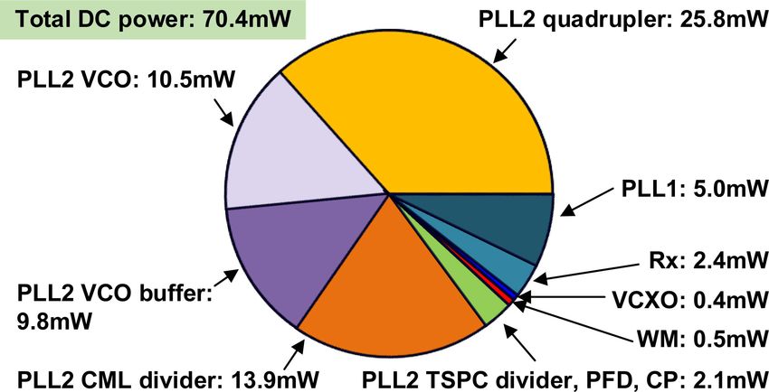
WANG et al.: TERAHERTZ MOLECULAR CLOCK ON CMOS USING HIGH-HARMONIC-ORDER INTERROGATION                                                             567

   Existing technologies do not completely fulfill the cur-                    first-order dispersion curve probing approach adopted by the
rent needs. The widely adopted oven-compensated crys-                          CSMC [34], [35].
tal oscillators (OCXOs) [11], [12] and MEMS oscillators                           In this article, a new CSMC locking to a high-odd-order
(OCMOs) [13]–[15] isolate the resonators from the sur-                         dispersion curve is demonstrated [36]. It also references the
rounding environment using a heated oven. The clock fre-                       231.061-GHz spectral line of OCS molecules. By performing
quency is further regulated by the temperature compensation                    a third-order derivative on the asymmetric line profile, the new
[16], [17]. The OCXO/OCMO provide decent temperature                           dispersion curve generated by the clock exhibits less temper-
stability of 10−7 ∼ 10−8 over the full temperature range                       ature dependence, and thus, the medium-/long-term stability
(−20 ◦ C ∼ +70 ◦ C) [11], [12]. However, their dc power is                     of the clock is significantly improved. In this 65-nm CMOS
at watt level in steady-state and is even higher during startup.               chip, a high-order spectroscopic system is implemented with
Alternatively, chip-scale atomic clocks have been developed                    enhanced sensitivity and signal purity. In the experiments, the
[18]–[20]. They are referenced to the electronic transitions of                CSMC achieves Allan deviations of σ y = 3.2 × 10⁻¹⁰ @τ =
Alkali atoms [e.g., rubidium (85Rb) or Cesium (133 Cs)]. The                   1 s and σ y = 4.3 × 10⁻¹¹ @τ = 103 s. Compared with the
utility of coherent population trapping (CPT) [21] and micro-                  prior CSMC [34], [35], an ∼8× stability improvement is
fabricated vapor cell [22] enables significant miniaturization                 obtained with a similar dc power of 70.4 mW. In addition,
and power reduction. The CSAC in [23] achieves a stability                     a single-chip realization is achieved through employing a
of ±1 × 10⁻⁹ within −10 ◦ C ∼ +70 ◦ C while only consum-                       pair of slot array couplers as an effective chip-to-molecular
ing 60-mW dc power. However, the CSACs possess several                         cell interface. It results in further packaging simplification
disadvantages.                                                                 and cost reduction. This article is organized as follows.
   1) A high cost due to sophisticated optical-electrical con-                 In Section II, the impacts of transmission baseline tilting
       struction. The required vertical cavity surface emitting                and the high-order molecular probing scheme are illustrated.
       laser (VCSEL) with precise 894.6-nm (D1) or 852.3-nm                    In Section III, the architecture of CSMC enabling the probing
       (D2) laser wavelength for 133 Cs atom probing has low                   scheme is presented. Section IV discusses the details of the
       yield [24]. Advanced MEMS and packaging technolo-                       circuit blocks. Then, Section V presents the clock packaging
       gies are applied for the tight integration of VCSEL, laser              and the experiment results. Section VI concludes this article
       detector, micro-fabricated vapor cell, and microwave                    with a comparison with the other state-of-the-art time-keeping
       circuitry.                                                              devices.
   2) Susceptibility to external magnetic fields due to the
       strong magnetic dipole of electron spins. As a result, all                        II. T RANSMISSION BASELINE T ILTING AND
       CSACs are equipped with a magnetic shield to alleviate                              H IGH -O DD -O RDER D ISPERSION C URVES
       the problem [25].                                                          A simplified schematic of CSMCs is shown in Fig. 1(a).
   3) A slow startup procedure. After a cold start, the clock                  A wavelength modulated THz probing signal VWM (t) is gen-
       package should be heated to around 80◦C for Alkali                      erated by a THz transmitter (Tx) referenced to a voltage-
       metal evaporation and then temperature-stabilized with                  controlled crystal oscillator (VCXO). The VCXO determines
       mK-level accuracy to ensure precise laser wavelength.                   the short-term clock stability [see Fig. 1(b)]. The instantaneous
       For instance, the Microsemi SA.45s CSAC needs 3 min                     frequency f p (t) [see Fig. 2(a)] of VWM (t) is expressed as
       for its startup procedure [26].
                                                                                                   f p (t) = f p +  f sin(2π f m t)               (1)
   Recently, the rotational spectra of polar gaseous molecules
in the terahertz range emerge as new physical references                       where f p is the center frequency, f m is the modulation fre-
for clock stabilization [27]. A rotational spectral line could                 quency, and  f is the frequency deviation. The gas absorption
have a high quality factor (∼106 ) and strong absorption                       coefficient α( f ) of the selected spectral line has a Lorentzian
intensity. Meanwhile, THz spectrometers on CMOS have been                      profile due to the pressure broadening [37], [38], which can
demonstrated [28]–[32]. Thus, low-cost clocks at chip scale                    be decomposed into a complex form as follows:
and with “atomic” clock grade stability become possible. The
                                                                                                            f h2
first chip-scale molecular clock (CSMC) chipset on 65-nm                              α( f ) = α p 2
CMOS locks to the 231.061-GHz rotational spectral line of                                           f + ( f − f 0 )2
                                                                                                   h
carbonyl sulfide (16 O12 C32 S) molecules in gas phase [33],                                                 1                    1
                                                                                             =β                         +                      (2)
[34]. It presents an Allan deviation of σ y = 3.8 × 10⁻¹⁰ with                                       f h + ( f − f 0 )i   f h − ( f − f 0 )i
an averaging time τ = 103 s and a 66-mW dc power. It enables                   where α p is the peak absorption coefficient in the spectral
a fast startup and all-electronic configuration potentially                    line center f 0 , f h is the half-width at half-maximum of a
leading to dramatic cost reduction compared with CSACs.                        specific spectral line, and the coefficient β = α p f h /2. After
However, its medium-/long-term stability with the presence                     the wave–molecule interaction, the intensity of the probing
of temperature fluctuation is degraded by the tilting of its                   signal is periodically modulated, as shown in Fig. 2(a). Then,
spectroscopic transmission baseline. Such tilting is caused                    a THz square-law detector [see Fig. 1] converts the intensity
by the inevitable, uneven frequency response of the THz                        fluctuation into the baseband signal I (t)
spectrometer and the molecular cell. In Section II, we show
that it leads to a spectral line profile with a temperature-                               I (t) = I0 · e−α( f p (t ))L
dependent asymmetry, which cannot be corrected by the                                            ≈ I0 · (1 − α( f p +  f sin(2π f m t))L)         (3)

          Authorized licensed use limited to: MIT Libraries. Downloaded on January 28,2021 at 22:43:28 UTC from IEEE Xplore. Restrictions apply.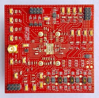
568                                                                              IEEE JOURNAL OF SOLID-STATE CIRCUITS, VOL. 56, NO. 2, FEBRUARY 2021

                                                                                Fig. 2. WMS. (a) Harmonic generation while probing the spectral line with
                                                                                a wavelength-modulated signal. (b) Mathematical derivatives of the Lorentz
                                                                                profile and the simulated odd-order dispersion curves with  f = 100 kHz
                                                                                and 1 MHz, respectively. f m = 0.1 ×  f . The amplitude is normalized. The
                                                                                polarization is aligned for a better comparison.

                                                                                absorption coefficient α( f ) in (2) can be expressed as

Fig. 1.   High-order molecular probing CSMC. (a) Simplified schematic.          d N α( f )                             (−1) N
(b) Clock stability in the short, medium, and long terms.                                  = N! · i N
                                                                                                      · β ·
                                                                                  df N                        ( f h + ( f − f 0 )i ) N+1

                                                                                                                                   1
                                                                                                                    +                              .   (6)
where I0 is the baseband signal without the gas absorp-                                                               ( f h − ( f − f 0 )i ) N+1
tion, and L refers to the path length of the molecular cell.                      While the center frequency of probing signal coincides with
α( f )L  1 is assumed in (3). Note that I (t) has abundant                     the spectral line center f p = f 0 , (6) can be written as
harmonics of f m . Correspondingly, (3) can be decomposed
                                                                                        d N α( f )                 N! · i N · β
as                                                                                           N                    =      N+1
                                                                                                                                  ((−1) N + 1). (7)
                                                                                        df          f = f p = f0     f h
                      ∞
       I (t) ≈ I0 1 −     VL K ,N ( f p ) cos(2π N fm t)   (4)                     As a result, while f p = f 0 , all the odd-order derivatives
                          n=0
                                                                                equal 0. Accordingly, (5) indicates that the baseband signal
                                                                                I (t) only has even order harmonics of fm , which is shown
where VL K ,N ( f p ) is the Nth Fourier component of the                       in Fig. 2(a). Since VL K ,N ( f p ) is 0 for all the odd-order
baseband signal at f p . N ∈ {1, 2, . . . ∞}. By assuming                       harmonics, the odd-order dispersion curves exhibit a zero-
 f  f FWHM , where f FWHM = 2 f h is the full-width at                        crossing point at f p = f 0 [see Fig. 2(b)], which provides
half-maximum of the spectral line, and VL K ,N ( f p ) can be                   the amplitude and polarization of frequency feedback control.
expressed as [39], [40]                                                         Hence, the odd-order dispersion curves can be adopted in
                                                                               CSMCs [27]. With a small frequency deviation [e.g.,  f =
                             21−N       N
                                     n d α( f )                                100 kHz  f FWHM = 1.47 MHz [34] in Fig. 2(b)], the
         VL K ,N ( f p ) ∝ L      f       N            .              (5)
                              N!        df        f = fp                        dispersion curves match well with the mathematical Nth-order
                                                                                derivative of the spectral line profile. However, a large  f is
    VL K ,N ( f p ) is proportional to the Nth-order derivative of              generally used for a higher loop gain and SNR. As shown in
α( f ) in (5). In Fig. 1(a), with the switch K “open,” VL K ,N ( f p )          Fig. 2(b), the dispersion curves deviate from the math with
is measured by a phase-sensitive lock-in detector. By sweeping                   f = 1 MHz. For more details on wavelength modulation
 f p , VL K ,N ( f p ) can be recorded as the Nth-order dispersion              spectroscopy (WMS) with a large  f , Wahlquist [41] and
curve [see Fig. 2(b)]. The Nth-order derivative of the gas                      Arndt [42] gave thorough analyses. Then, by “closing” the

           Authorized licensed use limited to: MIT Libraries. Downloaded on January 28,2021 at 22:43:28 UTC from IEEE Xplore. Restrictions apply.
WANG et al.: TERAHERTZ MOLECULAR CLOCK ON CMOS USING HIGH-HARMONIC-ORDER INTERROGATION                                                                       569

                                                                                    Fig. 4.      Temperature dependence of molecular clock. (a) Simulated
                                                                                    231.061-GHz line profile inside the gas cell under −40 ◦ C–105 ◦ C. (b) Sim-
Fig. 3. Baseline tilting induced frequency drift. (a) Asymmetric spectral line      ulated frequency drift of the first- and third-order lockings of CSMCs under:
profile due to the baseline tilting. (b) First-order dispersion curve shifted by    1) a baseline tilting of 10−5 –10−3 dB/MHz (or 0.01–1 dB/GHz, which
the offset voltage Voffset due to the baseline tilting. (c) High-order dispersion   is common in the THz transceivers) and 2) a temperature variation of
curve stands invariant under the baseline tilting. Thigh , Tmedium , and Tlow       −40 ◦ C–105 ◦ C. In the simulation, f m = 100 kHz, and  f = 1.25 MHz.
stand for the high, medium, and low temperatures.

switch K in Fig. 1(a), the CSMC locks to the zero-crossing                          Voffset generated from the first-order derivative applied on
point f p = f0 of the selected odd-order dispersion curve. After                    the tilted baseline and consequently possesses a temperature-
the locking, the clock stability in the medium term is inversely                    dependent zero-crossing point, as shown in Fig. 3(b). Besides
proportional to the Q × SNR product [27] [see Fig. 1(b)],                           the line profile, the slope of the baseline tilting also changes
where Q refers to the quality factor of the spectral line. With                     under the PVT variation, partly due to the thermal contrac-
a fixed Q, a CSMC with higher SNR presents better medium-                           tion/expansion of the molecular cell, which further complicates
term stability.                                                                     the variation of the zero-crossing point. Therefore, a CSMC
    Fig. 1(b) reveals that the clock medium-/long-term stability                    locking to the first-order dispersion curve suffers from the
depends on multiple factors, including the baseline tilting, tem-                   medium-/long-term instability [34].
perature, electrical field, and magnetic field. Here, the baseline                     In comparison, locking to a high-odd-order dispersion curve
tilting issue is addressed by a high-order locking scheme,                          generates a near-zero offset voltage Voffset due to the high-
whereas the other issues will be discussed in Section V.                            order derivative. As shown in Fig. 3(c), the zero-crossing
Theoretically, the spectral line profile is highly symmetric [37].                  point of the high-odd-order dispersion curve stays invariant
However, the frequency response of the THz spectrometer is                          under the temperature variation. A numerical simulation of
not completely flat, and the limited impedance matching at the                      the clock frequency over the slope of the baseline tilting and
chip-molecular cell interface introduces a standing wave inside                     the temperature variation is conducted in Fig. 4(b). Under a
the molecular cell. These cause a tilting in the baseline of                        fixed baseline tilting of 10−4 dB/MHz, at 25 ◦ C, the first- and
the transmission spectrum, as shown in Fig. 3(a). In addition,                      third-order lockings lead to frequency drifts of 6.5 × 10⁻⁹ and
simulated by spectralcalc [43], the peak absorption intensity of                    3.4 × 10⁻¹⁰ , respectively. A 19× improvement is achieved
the 231.061-GHz spectral line inside the WR-4.3 waveguide                           for the third-order locking. Meanwhile, the baseline-tilting-
gas cell changes from 49.7% at −40 ◦ C to 17.2% at 105 ◦ C,                         induced temperature dependencies are 4.9 × 10⁻¹¹ /◦ C and
while the linewidth f FWHM increases from 1.17 to 1.33 MHz,                         0.4 × 10⁻¹² /◦ C for the first- and third-order lockings,
as shown in Fig. 4(a). Thus, the superposition of the symmetric                     respectively. The third-order locking reduces the temperature
OCS transition and the tilted baseline results in a temperature-                    dependence by 126×. In addition, due to the simplified
dependent asymmetric line profile [see Fig. 3(a)]. As a result,                     baseline model here, the fifth-order locking behaves similarly
the first-order dispersion curve contains an offset-voltage                         as the third-order case does. This is also confirmed by the

             Authorized licensed use limited to: MIT Libraries. Downloaded on January 28,2021 at 22:43:28 UTC from IEEE Xplore. Restrictions apply.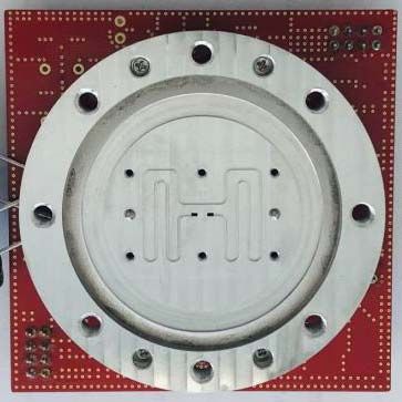
570                                                                                IEEE JOURNAL OF SOLID-STATE CIRCUITS, VOL. 56, NO. 2, FEBRUARY 2021

                                                                                  modulation also needs to be minimized to avoid the harmonic
                                                                                  artifact components in the baseband I (t). In this design,
                                                                                  instead of the frequency shift keying (FSK) used in [34],1
                                                                                  a sinusoidal wavelength modulation is realized by applying
                                                                                  a digitally synthesized analog modulation signal onto the
                                                                                  voltage-controlled oscillator (VCO) of the second-stage PLL
                                                                                  (see Fig. 7) using a wavelength modulator (WM) (see Fig. 8).

                                                                                  C. Integrated Low-Loss Chip-to-Molecular Cell Interface
                                                                                     The molecular cell hermetically sealed the OCS gas sample
                                                                                  inside a 14-cm-long meandering WR-4.3 waveguide. In the
                                                                                  first CSMC prototype, a pair of lossy (L ≈ 10 dB) off-chip
                                                                                  waveguide E-plane quartz probes [49] were used and were the
Fig. 5.   System architecture of the presented CSMC.
                                                                                  SNR bottleneck [34]. It also results in high assembly variation
                                                                                  and manufacturing costs. To solve this issue, a pair of on-
                                                                                  chip slot-array couplers are innovated with reduced signal loss,
measurement in Table I. Therefore, Fig. 4 does not show the
                                                                                  enhanced Tx–Rx isolation, and a compact packaging structure.
fifth-order results.
                                                                                  It is a key enabler for a monolithic, low-cost CSMC.
   We note that the high-order locking was also previously
applied in our instrument-based lab-scale OCS clock prototype
[27]. In the 1970s, Wineland et al. [44], [45] implemented a                      D. High Linearity THz Detection
lab-scale ammonia clock, which referenced to the inversion                           The THz detector and the variable-gain amplifier (VGA)
spectrum of the molecules at 23.8 GHz [46], [47]. Similar                         in Fig. 9 convert the FM-modulated intensity fluctuation of
high-order locking was adopted. Next, we present our technical                    THz probing signal to the baseband I (t). The THz receiver
details that enable high-order molecular locking in a THz                         chain should have not only high responsivity and low noise
monolithic integrated circuit.                                                    equivalent power (NEP) but also high linearity to handle the
                                                                                  even-order harmonic components in I (t), which reaches the
                   III. S YSTEM A RCHITECTURE                                     peak amplitude at locking [see Fig. 2(a)]. Correspondingly,
  The system architecture of the CSMC chip is shown in                            the chip is designed to address the distortion due to saturation
Fig. 5. The key design challenges, as well as the corresponding                   (see Fig. 9).
solutions, are summarized as follows.
                                                                                  E. Phase-Sensitive Lock-In Detection With Low Noise and
A. Low-Power, Broadband, and High-Quality THz Signal                              Offset
Generation                                                                           A harmonic-rejection lock-in detector (HRLKD) [see
   The power saturation threshold inside the gas cell of the                      Fig. 11] demodulates the desired Nth-order harmonic to dc
probing signal is ∼50 μW [27]. The power efficiency is                            (VL K ,N in Fig. 5). Low output flicker noise of HRLKD
critical since the THz source consumes the majority of the                        is desired to reduce the required gain of preceding VGA,
total dc power of CSMC. In addition, the rotational spectrum                      thus improving the Rx linearity. Meanwhile, since the inter-
of OCS exhibits a frequency interval of 12.16 GHz [43]. There                     modulation of the lock-in detector would introduce unwanted
are two adjacent lines located at 218.903 and 243.218 GHz,                        harmonics and noise, an effective harmonic rejection is pre-
respectively. Due to the PVT issue, the central frequency of                      ferred. Finally, the output dc offset of the lock-in detector is
the CMOS spectroscopic system can differ by ±10%. Thus,                           translated into the clock drift, hence should be minimized.
a wide PLL tuning range (e.g., ≥24 GHz) is preferred. It does                        Finally, after the dc amplification and filtering by off-chip
not only ensure the spectral line coverage but also reduces the                   op-amps (GDC in Fig. 5), the error signal VL K ,N is fed back to
sensitivity of clock performance over PVT. Furthermore, the                       the differential frequency control nodes of VCXO. This way,
phase noise of the probing signal dominates the spectroscopic                     the chip achieves locking to the zero-crossing point of the
SNR through a PM-to-AM noise conversion [48]. In this                             Nth-order dispersion curve. The molecule-regulated 60-MHz
work, driven by a 60-MHz VCXO, a 231-GHz two-stage                                VCXO is used as the CSMC output.
phase-locked loop (PLL) generates the desired probing signal,
as shown in Fig. 6.                                                                     IV. D ESCRIPTION OF C RITICAL C IRCUIT B LOCKS
                                                                                     In this section, we present the design details of several
B. High-Precision THz Wavelength Modulation                                       critical building blocks in Fig. 6.
  With a MHz-level  f and a center frequency f 0 =
231.061 GHz, f p only fluctuates ±10−5 for the wavelength
                                                                                    1 The FSK scheme, by periodically comparing two discrete points at the
                                                                                  spectral-line slopes, only generates square-wave baseband output, of which the
modulation. A tunable  f is desired to achieve optimal                           high-order harmonics do not contain additional information about the shape
SNR. The frequency distortion of the sinusoidal wavelength                        of the spectral line.

             Authorized licensed use limited to: MIT Libraries. Downloaded on January 28,2021 at 22:43:28 UTC from IEEE Xplore. Restrictions apply.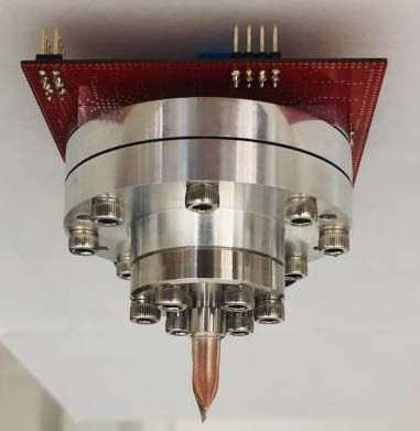
WANG et al.: TERAHERTZ MOLECULAR CLOCK ON CMOS USING HIGH-HARMONIC-ORDER INTERROGATION                                                                571

Fig. 6.   Schematic of cascaded two-stage 231.061-GHz PLL with a 60-MHz on-chip VCXO.

A. Cascaded Two-Stage 231.061-GHz PLL
    The schematic of the 231-GHz cascaded two-stage PLL is
shown in Fig. 6. A 60-MHz on-chip VCXO with off-chip
quartz crystal [50] is implemented as the PLL reference. It has
a frequency tunability of 3 kHz/V and a differential control
node for the input common-mode noise rejection. The first-
stage 3.21-GHz fractional-N PLL (PLL1) provides a tuning
resolution of 24 bit. When the CSMC is locked, it allows
for a digitally set output frequency (around 60 MHz) with a
relative frequency step of 6 × 10⁻⁸. Next, referenced to PLL1
(3.21 GHz ÷ 16 = 200.6 MHz), the second-stage integer-
N PLL (PLL2) is in charge of high-efficiency, broadband,
and high-quality THz signal generation. To this end, a cross-
coupled 57.77-GHz VCO and a slot-balun-based frequency
quadrupler (×4) [32] are adopted in PLL2, as shown in
Fig. 7(a). The simulation [see Fig. 7(b)] shows a 3-dB power
RF bandwidth of 23.4 GHz (26% wider than [34]) and a peak
RF power of −4.4 dBm (∼2× higher than [34]) with a dc
power consumption of 46 mW (similar to [34]). In addition,
an inductor-less current-mode logic (CML) divider (÷8) is
employed to ensure the wideband PLL locking [51].
    Compared with the single-stage fractional-N PLL with built-
                                                                                  Fig. 7. 57-GHz VCO and 231-GHz quadrupler of PLL2. (a) Schematic.
in FSK modulation in [34], the two-stage PLL architecture                         (b) Simulated RF output power and tuning range. (c) Simulated frequency
brings the following advantages. First, a steady-state, low-                      sensitivity of wavelength modulation through VAR2.
frequency fractional-N PLL ensures good frequency resolu-
tion, low – noise, and low spur level. The – noise
and spurs are further reduced by the low-pass filtering of the                    a 12% locking range. The VAR2 is used for the wavelength
second-stage PLL loop. Second, an analog modulation signal                        modulation (±10−5 relative frequency change). For VAR2,
Vm is directly applied to the VCO2 of PLL2 [see Fig. 7(a)] in                     a large frequency sensitivity would result in a small signal
order to generate a sinusoidal wavelength modulation for the                      amplitude of Vm . In that case, to maintain a sufficiently
high-order locking. Note that a higher wavelength modulation                      high SNR of Vm , the modulator needs a higher dc power.
frequency f m is desired to reduce the impact of flicker noise in                 It also suffers from a worse spur rejection with a smaller
the THz detector. In Fig. 6, the cascaded PLL enables a high                      Vm . Therefore, besides choosing a minimum-size varactor for
 f m of 100 kHz because the PLL settling time is no longer a                      VAR2, a resistive source degeneration [see Fig. 7(a)] is used
limiting factor like that in [34]. Now, f m is only limited by                    to further reduce the tuning coefficient to 31.3 MHz/V [see
the molecule linewidth f FWHM [39]. The loop bandwidth of                         Fig. 7(c)]. The differential analog modulation signal Vm is
PLL2 is set as 10 kHz for a tradeoff between the PLL initial                      digitally synthesized by a WM, as shown in Fig. 8. The WM is
locking (larger bandwidth preferred) and the frequency pulling                    clocked by the 60-MHz VCXO. An 8-bit code of the 100-kHz
of the wavelength modulation (smaller bandwidth preferred).                       sinusoidal waveform is generated by the digital sine code
                                                                                  generator. A phase tunability with 360◦ range and 0.6◦ step
                                                                                  size has been included for the phase synchronization of the
B. High-Precision Wavelength Modulator                                            lock-in demodulation in Rx. A reference clock f ref = 4· N · f m
  The VCO2 in PLL2 [see Fig. 7(a)] has two frequency-                             for the lock-in detector (HRLKD) is also provided by the
tuning nodes. The VAR1 has a frequency sensitivity of                             WM. Next, the 8-bit code drives a differential digital-to-
22.7 GHz/V, which serves for the broadband PLL locking with                       analog converter (DAC) to generate a rail-to-rail differential

             Authorized licensed use limited to: MIT Libraries. Downloaded on January 28,2021 at 22:43:28 UTC from IEEE Xplore. Restrictions apply.
572 IEEE JOURNAL OF SOLID-STATE CIRCUITS, VOL. 56, NO. 2, FEBRUARY 2021
Fig. 8. WM. (a) Schematic. (b) Simulated Vm waveform. (c) Amplitude of Vm versus the control code D. (d) Simulated spectrum of Vm while D = 7.
(e) Simulated noise voltage of the 100-kHz modulation signal, while D = 7.
Fig. 9. Schematics of THz detector and VGA.
sinusoidal signal at fm = 100 kHz. After the low-pass filter- C. THz Detector and Baseband VGA
ing, the amplitude of Vm is controlled by the attenuator with The schematics of the THz square-law detector and VGA
a 3-bit control code D for the desired f . are shown in Fig. 9. A pseudo-differential nMOS transistor
The simulated waveform of the modulation signal Vm is pair biased under the sub-threshold region is used for THz
shown in Fig. 8(b). The amplitude of Vm is adjustable in square-law detection. Compared with a single-ended design,
a log-scale, as shown in Fig. 8(c). The simulated worst it provides better common-mode noise rejection. With a drain
case spur rejection (with the minimum Vm amplitude of current of 49 μA, the simulated responsivity and the NEP of
25.8 mV, while D = 7) is better than 55 dB, as shown in the THz detector, with a 231-GHz input and 100-kHz baseband
Fig. 8(d). It is noteworthy that both the Vm spurs (which frequency, are 11.0 kV/W and 11.7 pW/Hz0.5 , respectively.
increase with |Vm |) and any nonlinearity in the frequency- The 231.06-GHz probing signal injected into the THz detector
tuning coefficient of VAR2 [which decreases with |Vm |, see has an RF power of ∼−22 dBm, which induces an output
Fig. 7(c)] result in harmonic artifacts in the wavelength baseband swing of ∼23 mV. Thus, the THz detector still
modulation, which will be translated into clock frequency works in the small-signal status. The VGA provides 13∼65-dB
drift. In our design, an optimal amplitude of Vm is chosen tunable gain to adapt to the baseband output of the THz
to minimize such a drift. One future solution is to use detector. The VGA consists of two cascaded single-stage
a digitally pre-distorted modulation waveform to eliminate op-amps. A high-resistive, transistor-based feedback structure
the harmonic√artifacts. Finally, the worst case noise floor and a 10-pF on-chip capacitor are used to avoid off-chip ac
is 0.32 μV/ Hz at 1-Hz offset frequency, as shown in coupling components and enhance the isolation of the THz
Fig. 8(e). The associated worst case SNR of the WM is 95 dB, detector and VGA from external interference. In addition,
which is sufficiently high to avoid limiting the system overall a high loop gain of at least 104 is desired for CSMC to
SNR. suppress the frequency error of VCXO [27]. The VGA is a
Authorized licensed use limited to: MIT Libraries. Downloaded on January 28,2021 at 22:43:28 UTC from IEEE Xplore. Restrictions apply.WANG et al.: TERAHERTZ MOLECULAR CLOCK ON CMOS USING HIGH-HARMONIC-ORDER INTERROGATION 573
VGA gain in our CSMC architecture. To solve this issue,
an HRLKD is innovated, as shown in Fig. 10(b).√It replaces the
gm cells with a set of ratioed resistors (R:R/ 2:R). Similar
to the conventional scheme in Fig. 10(b), at the Vout node,
the currents in the three paths recombine constructively when
f in = f ref and cancel at f in = 3 f ref and f in = 5 f ref .
The output capacitor C performs additional low-pass filtering.
Since resistors and MOS switches exhibit near-zero flicker
noise, the proposed HRLKD is better suited for our CSMC.
Fig. 11(a) presents a detailed schematic of the HRLKD. The
input of HRLKD is buffered with a source follower for its low
output impedance. Meanwhile, differential signaling is used
to suppress unwanted even-order-harmonic responses too. The
quadrature clock ( f ref = 4· N · f m ) of HRLKD is obtained from
the reference clock generated in the WM described previously
[see Fig. 8(a)]. By specifying the harmonic index N, the
CSMC can lock to the desired Nth-order dispersion curve.
The simulated harmonic-rejection ratio in Fig. 11(b) is >80 dB
for the second- to sixth-order harmonics. The simulated output
noise floor is shown in Fig. 11(c). Note that the flicker noise
of the source follower is upconverted and is not translated
into the output of HRLKD. The current noise floor near dc is
dominated by the noise of output resistance Rout of HRLKD.
Fig. 10. Harmonic-rejection scheme. (a) Phasor diagram of the classic
third- and fifth-order harmonic-rejection schemes. (b) Comparison between
Since the ratioed resistors inside the HRLKD adopt R of
the conventional harmonic-rejection mixer and the proposed resistive-based 100 k , the output resistance Rout is 37 k . Next, we note
lock-in detector. that the output dc offset voltage of the HRLKD also induces
clock drift, with a relative clock frequency dependence of
5.0 × 10⁻¹¹/μV in our simulation. Due to the 50% duty cycle
key contributor to the overall loop gain. However, as shown in
of the HRLKD clock, the measured output dc offset voltage
Fig. 2(a), when locking to the spectral line center ( f p = f 0 ),
is lower than 10 μV, and its low sensitivity to temperature
in the THz detector output, the near-zero odd-order harmonics
causes negligible clock instability. Finally, we note that the
at f m , 3 f m , 5 f m , . . . are accompanied with strong even-order
output resistance of HRLKD and the input capacitance of GDC
harmonics at 2 f m , 4 f m , 6 f m , . . . If the gain of VGA is too
[see Fig. 11(a)] determine the dominant pole of the CSMC
high, the even-order harmonics drive the VGA to saturation.
feedback control loop. A low dominant pole is achieved by
This is a critical issue that limits the maximum gain of VGA.
using the Miller capacitor C2 in GDC.
As a result, the loop gain of CSMC is distributed between the
baseband VGA and a dc-gain stage (GDC in Fig. 5). Inside E. Chip-Integrated Slot-Array-Based THz Waveguide Coupler
the VGA, a 5-bit resistor bank R0 is used for gain control,
Low-loss chip-to-molecular cell interface is critical to main-
and a common-mode feedback (CMFB) circuit is implemented
tain optimal systematic SNR and avoid the need for high
to set the operation point of the output node for large output
THz power generation in the CSMC. Prior waveguide E-plane
swing. Another potential solution to address the gain limit of
quartz probes [49] and dielectric-resonator-based couplers [56]
VGA is to use a N-path notch filter [52], which eliminates
rely on off-chip components for THz-wave coupling. They
the even-order harmonics. However, more attention needs to
present high insertion loss, high assembly cost, and also
be paid for extra filtering of up-converted harmonics if this
large sample-to-sample variation. On-chip integrated dipole
scheme is to be used.
coupler was demonstrated [57], but it requires not only wafer
thinning to tens of μm but also through-chip vias to suppress
D. Harmonic-Rejection Lock-In Detector the substrate mode, which is not available in many CMOS
Conventional lock-in detectors without harmonic rejection processes. In this work, a pair of slot array couplers are
[53], [54] suffer from the interference and noise folding at innovated as the chip-to-molecular cell interface. Its 3-D
the unwanted harmonics of the reference clock f ref , which structure is shown in Fig. 12(a), where four double-slot
degrades the clock stability. Fig. 10 shows the schematic and radiators fed by a slot balun [48] radiate downward into the
phasor diagram of a classic third- and fifth-order harmonic- un-thinned silicon substrate (T = 304.8 μm). The WR-4.3
rejection schemes [55], which utilizes switches driven by a metal waveguide opening (1.092 × 0.546 mm2 ) is attached
quadrature-phase clock and ratioed transconductance gm to directly to the backside of the CMOS chip. With optimal slot
eliminate the third- and fifth-order harmonics of f ref . gm is array dimension, electromagnetic mode matching between the
provided by the MOS transistors biased at saturation region. chip-launched fields at the silicon-air interface and the TE10
However, these biased transistors exhibit excessive flicker mode in the metal waveguide is achieved and enables efficient
noise, which cannot be well suppressed due to the limited coupling.
Authorized licensed use limited to: MIT Libraries. Downloaded on January 28,2021 at 22:43:28 UTC from IEEE Xplore. Restrictions apply.574 IEEE JOURNAL OF SOLID-STATE CIRCUITS, VOL. 56, NO. 2, FEBRUARY 2021
Fig. 13. Simulation results of slot array coupler. (a) Transmission and
reflection losses. (b) Tx–Rx isolation. (c) Frequency drift at varying ϕ (with
−60-dB Tx–Rx isolation). (d) Frequency drift at varying isolation levels (with
ϕ = 90◦ or 270◦ ).
launched waves are concentrated in the substrate, rather than
the front side of the chip, due to the high permittivity of
silicon. As a result, the slot array coupler is insensitive
Fig. 11. HRLKD. (a) Detailed schematic. (b) Simulated harmonic-rejection to the bond wires and external components on the PCB.
ratio with f ref = 100 kHz. (c) Output noise floor of the HRLKD output A minimum of 5.2-dB transmission loss and a 21% fractional
VL K ,N versus the noise floor of source follower VSF and the thermal noise
of output resistance Rout . 3-dB bandwidth are obtained in the simulation, as shown in
Fig. 13(a). A 5-dB loss reduction is achieved compared with
that in [34], resulting in ∼20-dB system SNR improvement.
The loss can be further reduced by ∼3 dB if the resistivity of
the silicon substrate is increased as the cases of, for instance,
CMOS SOI processes [58].
It is noteworthy that an undesired clock drift can be
generated by any Tx-to-Rx leakage through the substrate; it
is sensitive to the phase difference ϕ between the above
leakage signal and the normal transmitted signal through
the gas cell [see Fig. 13(c)]. Since ϕ can be affected by
the thermal contraction/expansion of the gas cell, the above
Tx-to-Rx leakage should be minimized. In our work, that is
achieved by the endfire nulling of the 2×2 array configuration
[see Fig. 12(a)]. As shown in Fig. 13(b), excellent Tx-to-Rx
isolation of 60 dB is obtained in the simulation. In the worst
case [90◦ or 270◦ phase difference in Fig. 13(c)], the 60-dB
isolation leads to a frequency drift of 1.8 × 10⁻⁹ for the first-
order locking and 0.9 × 10⁻⁹ for the third-order locking [see
Fig. 13(d)]. In the future, even higher isolation in CSMC may
be achieved by an active cancellation technique [59]. Since
the presented slot-array coupler requires no off-chip compo-
nent nor wafer thinning, the clock packaging is significantly
Fig. 12. Slot array couplers. (a) 3-D structure and (b) simulated electrical- simplified (more details given in Section V-A).
field distribution at 231 GHz.
V. E XPERIMENTAL R ESULTS
Fig. 12(b) shows the simulated electrical-field distribution
of the slot array coupler pair. Port 1 and Port 4 are WR- A. Chip Packaging With Molecular Gas Cell
4.3 waveguides with the TE10 mode. Port 2 and Port 3 are The chip is fabricated using TSMC 65-nm bulk CMOS tech-
on-chip shielded microstrip line with quasi-TEM mode. The nology. The die photograph is shown in Fig. 14. The chip has a
Authorized licensed use limited to: MIT Libraries. Downloaded on January 28,2021 at 22:43:28 UTC from IEEE Xplore. Restrictions apply.WANG et al.: TERAHERTZ MOLECULAR CLOCK ON CMOS USING HIGH-HARMONIC-ORDER INTERROGATION 575
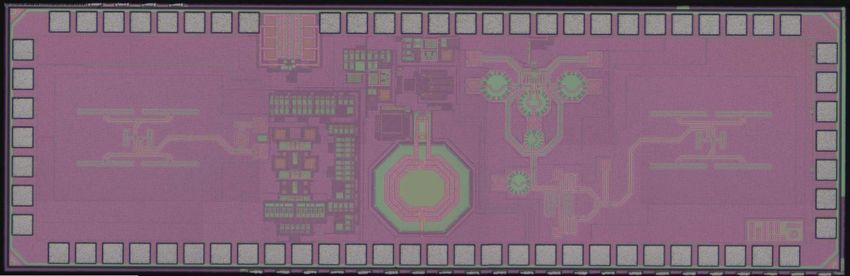
Fig. 14. Die photograph of the CMOS molecular clock chip.
Fig. 16. DC power consumption breakdown.
TABLE I
PARAMETERS OF THE M EASURED O DD -O RDER D ISPERSION C URVES
is first evacuated to high vacuum through the OCS inlet/outlet
with a cutoff frequency much higher than the probing signal
to prevent the signal leakage. Next, the standalone gas cell
without the CMOS chip is baked under a temperature of
150 ◦ C for 72 h. Then, OCS molecules are injected with
a pressure of 10 P. Finally, a copper tube connecting the
molecular cell with the vacuum system is pinched-off, so as to
realize a standalone molecular cell with hermetic sealing [see
Fig. 15(a)]. The CMOS chip is glued on top of the aluminum
base with two waveguide openings of the molecular cell. The
special mechanical structure on the aluminum base ensures
an alignment tolerance of ±20 μm. Then, the CMOS chip is
wire-bonded to a PCB with other periphery circuits (e.g., GDC
and the bias circuits). We emphasize that the current packaging
is not optimized for the minimum form factor. The ultimate
limiting factor of the CSMC size is the THz waveguide itself,
which has a volume of 20×16×1.1 mm3 . With micromachined
THz waveguide technologies in the substrate, such as silicon
[61], low-cost CSMC with a size of 1 cm3 is feasible. The
CSMC chip consumes a total dc power of 70.4 mW, of which
a breakdown is given in Fig. 16. Out of that, ∼88% (i.e.,
62 mW) is from the PLL2 used for THz power generation.
Fig. 15. Packaging of a CSMC module. (a) Gas cell and CMOS chip bonded
on PCB. (b) Hermetically sealed gas cell with optically transparent epoxy.
We see a decent room for dc power reduction. For instance,
as described in Section IV-E, the generated probing power can
be cut by ∼2× if a high-resistivity silicon substrate is used.
dimension of 4 ×1.25 mm2 and an un-thinned (305 μm), low-
resistivity (10 ·cm−1 ) silicon substrate. The packaged CSMC B. Electrical-Performance Characterization of the Chip
module is shown in Fig. 15(a). It contains an aluminum molec- The THz output power of the clock module is measured by
ular cell fabricated via computerized numerical control (CNC) connecting its WR-4.3 waveguide interface with an Erickson
milling. The meandering WR-4.3 waveguide has an optimum PM-5 power meter. As shown in Fig. 17(a), the peak output
length of 14 cm for the highest SNR [48]. As shown in power, including the loss of slot-array coupler (5.2 dB in
Fig. 15(b), the two WR4.3 waveguide apertures of the gas cell simulation), is −9.4 dBm at 231 GHz. The output has a 3-dB
are sealed by the optically transparent epoxy EPO-TEK 301-2 bandwidth of 22 GHz (9.5%) and a PLL locking range of
[60]. To avoid gas leakage and outgassing, the molecular cell 26 GHz (11.3%). The measured output power agrees well with
Authorized licensed use limited to: MIT Libraries. Downloaded on January 28,2021 at 22:43:28 UTC from IEEE Xplore. Restrictions apply.576 IEEE JOURNAL OF SOLID-STATE CIRCUITS, VOL. 56, NO. 2, FEBRUARY 2021
TABLE II
C OMPARISON TABLE OF H IGH -S TABILITY, M INIATURIZED C LOCKS
will be further discussed in Section V-C. At 231.061 GHz,
the measured phase noise is only 2 ∼ 3 dB worse than the
simulation: −62.3 dBc/Hz at a 100-kHz frequency offset and
−84.9 dBc/Hz at a 1-MHz frequency offset. Note that the
simulation includes the VCO noise, the thermal noise of gate
bias [Vgg in Fig. 7(a)], and the AM-to-PM noise conversion
due to non-linearity of 231-GHz quadrupler but excludes the
power supply noise. Hence, the off-chip power supply noise
is one factor that may degrade the PLL performance. As a
reference, in this work, Tektronix PWS 4323 with on-broad
capacitor array is used to power the chip. Next, after enabling
the wavelength modulation, the output spectrum of the probing
signal with different f ’s is shown in Fig. 17(c). f is
adjusted through the digital attenuator in Fig. 8.
Finally, the Rx performance is characterized by an external
VDI THz source with a tunable fm and a Stanford Research
System SR865A lock-in amplifier. At fm = 100 kHz, the
measured √ responsivity and NEP achieve 5.5 × 10⁵ V/W √ and
62.8 pW/ Hz, respectively. An NEP of 19.0 pW/ Hz is
Fig. 17. Measurement results of the spectroscopic Tx and Rx. (a) Measured derived after de-embedding the loss of the slot array coupler,
output RF power versus the simulated RF power, including the loss of slot and such performance is similar to state-of-the-art silicon-
array coupler. (b) Phase noise of first-stage PLL at 3.21 GHz and second-stage
PLL at 231.061 GHz without modulation. (c) Spectrum of THz probing signal
based THz detectors [64].
with modulation. Different f ’s are applied by specifying the attenuator code
D in WM. f 0 = 231.061 GHz. (d) Responsivity and NEP of Rx at 231 GHz. C. Characterization of the Clock System
The CSMC under an open-loop configuration is used as
the simulated results, which proves the effectiveness of the a spectrometer to measure the first-to-fifth order dispersion
slot-array coupler. Next, the phase noise of the 3.21-GHz PLL1 curves. In this configuration, the on-chip Tx and Rx are
output signal, measured by a Keysight N9020A spectrum enabled. A Tx probing signal with fm = 100 kHz and f =
analyzer, is −96.7 dBc/Hz at 100-kHz offset frequency and 2.5 MHz probes the spectral line in the molecular cell. The
−107.5 dBc/Hz at 1-MHz offset frequency [see Fig. 17(b)]. frequency deviation f = 2.5 MHz is selected experimentally
The phase noise of the 231.061-GHz PLL2 output, measured with the highest SNR × Q product, which is higher than f =
through a VDI even-harmonic mixer, is −60.7 dBc/Hz at a 1.25 MHz in Fig. 4 due to the broadening of power saturation
100-kHz frequency offset and −81.5 dBc/Hz at a 1-MHz effect [37]. By sweeping the PLL frequency, the multi-order
frequency offset. This is comparable with the THz sources dispersion curves are demodulated by the HRLKD, as shown
using coupled oscillator arrays [62], [63] that consume 10× in Fig. 18. Table I summarizes the measured dispersion curve
higher dc power. Nevertheless, the associated SNR limit due to parameters. For the first-order dispersion curve, an SNR of
a PM-to-AM noise conversion of the spectral line absorption 83.5 dB is obtained. Compared with [34], a 10.8-dB higher
[48] is estimated to be 84 dB. This is currently a major RF probing power is achieved by employing the low loss
limiting factor of the clock medium-term stability, which slot array coupler and an improved Tx design. In addition,
Authorized licensed use limited to: MIT Libraries. Downloaded on January 28,2021 at 22:43:28 UTC from IEEE Xplore. Restrictions apply.WANG et al.: TERAHERTZ MOLECULAR CLOCK ON CMOS USING HIGH-HARMONIC-ORDER INTERROGATION 577
Fig. 19. Photograph of the closed-loop CSMC setup and the measured Allan
deviation.
Fig. 18. Measured odd-order dispersion curves under an open loop configu-
ration of CSMC. The measurement setup: f m = 100 kHz and f = 2.5 MHz
(D = 3). VL K ,N are the dc output voltages of HRLKD.
due to a lower flicker noise enabled by a faster modulation
frequency f m , the low loss slot array coupler, and an optimized
square-law detector, the Rx reduces the NEP by 8×. Hence,
a 39.6-dB SNR enhancement is expected (if the saturation
effect is ignored). However, the measurement only presents
a 30.5 dB higher SNR (from 53 dB in [34] to 83.5 dB
in Table I). As shown in Section V-B, the SNR limited by
the Tx phase noise through PM-to-AM noise conversion is
84 dB, which is close to the 83.5-dB system SNR. Thus,
the Tx phase noise, instead of the link budget, determines
the threshold of SNR in the current system. In addition, it
can be clearly seen that the SNR and the amplitude Vamp
decrease in higher order dispersion curves. This degradation
comes from: 1) the high-order derivative of the line profile and
2) the frequency pulling of PLL, as mentioned in Section IV-A.
In addition, as expected, the third- and fifth-order dispersion
curves present much lower offset voltage Voffset . Even after
normalizing Voffset with the different Vamp ’s, the third- and
fifth-order curves are still two orders of magnitude better than
the first-order curve. It verifies the effectiveness of high-
order probing in dealing with the transmission-baseline tilting. Fig. 20. Sensitivity of the clock to environmental disturbances. (a) Mea-
Considering a tradeoff between the SNR and the offset voltage surement setup. (b) Raw data of temperature induced frequency drift.
Voffset , the third-order dispersion curve is selected for the (c) Temperature dependence with the second-order polynomial compensation.
(d) Frequency drift under a strong, externally applied magnetic field of 75 G.
closed-loop CSMC.
The setup and the measured Allan deviation of the closed-
loop third-order CSMC are shown in Fig. 19. The Allan devi- atomic clock (PRS10). With a unity gain loop bandwidth of
ation is measured by a Keysight 53230A frequency counter 5.5 mHz, the third-order CSMC exhibits an Allan deviation
referenced to a 10-MHz Stanford Research System Rubidium of 3.2 × 10⁻¹⁰ for an averaging time of τ = 1 s and
Authorized licensed use limited to: MIT Libraries. Downloaded on January 28,2021 at 22:43:28 UTC from IEEE Xplore. Restrictions apply.578 IEEE JOURNAL OF SOLID-STATE CIRCUITS, VOL. 56, NO. 2, FEBRUARY 2021 4.3 × 10⁻¹¹ for an averaging time of τ = 103 s. Compared CSMCs have faster startup time because there is no Alkali with the free-running VCXO, the medium-/long-term stability evaporation and temperature stabilization as those in CSACs at τ = 103 s is improved by almost three orders of magni- are needed. Finally, competitive 70.4-mW power consump- tude. Fig. 20(a) shows the measurement setup for the clock tion of the presented CSMC makes it suitable for power- temperature dependence and the magnetic field sensitivity. constraint applications. It should be noted that, as an emerging The temperature is controlled by a heater beneath the CSMC. technology, the CSMCs still have vast room for performance Without any temperature compensation, the CSMC frequency and efficiency improvement. That is particularly justified with drifts by ±5 × 10⁻⁸ over a temperature range of 27 ◦ C–65 ◦ C the recent advances in CMOS processes, which now offers [see Fig. 20(b)]. With an on-chip temperature sensor (see transistors with f max around 400 GHz [65], [66]. Therefore, Fig. 5) and a simple second-order polynomial compensation, a CSMC with atomic-clock-grade stability, cm3 volume, and the clock drift is reduced to ±3×10⁻⁹ , as shown in Fig. 20(c).
WANG et al.: TERAHERTZ MOLECULAR CLOCK ON CMOS USING HIGH-HARMONIC-ORDER INTERROGATION                                                                          579

[16] SiTime. Precision MHz Super-TCXOs SiT5000. Accessed: Jan. 3, 2020.           [43] Spectralcalc. High Resolution Spectral Modeling. Accessed:
     [Online]. Available:https://www.sitime.com/products                               Jan. 3, 2020. [Online]. Available: https://www.spectralcalc.com/
[17] SiTime. SiT5155, 0.5 ppm Super-TCXO for GNSS/GPS. Accessed:                  [44] D. J. Wineland, D. A. Howe, and H. Hellwig, “Special purpose
     Jan. 3, 2020. [Online]. Available:https://www.sitime.com/products                 atomic (molecular) standard,” in Proc. 8th Annu. Precise Time Mater.
[18] D. Ruffieux, M. Contaldo, J. Haesler, and S. Lecomte, “A low-power                Interval (PTTI) Appl. Planning Meeting. Held at Nav. Res. Lab., Pre-
     fully integrated RF locked loop for miniature atomic clock,” in IEEE              pared Goddard Space Flight Center, Greenbelt, MD, USA, Dec. 1977,
     ISSCC Dig. Tech. Papers, Feb. 2011, pp. 48–50.                                    pp. 429–448.
[19] Microsemi. Microsemi SA.45s Chip Scale Atomic Clock Datasheet.               [45] D. J. Wineland, D. A. Howe, and M. B. Mohler, “Results with the
     Accessed: Jan. 3, 2020. [Online]. Available: https://www.microsemi.               special-purpose ammonia frequency standard,” in Proc. 31st Annu. Symp.
     com/product-directory                                                             Freq. Control, Jun. 1977, pp. 562–573.
[20] H. Zhang et al., “29.4 ultra-low-power atomic clock for satellite constel-   [46] C. H. Townes, “Atomic clocks and frequency stabilization on microwave
     lation with 2.2×10⁻¹² long-term allan deviation using cesium coherent             spectral lines,” J. Appl. Phys., vol. 22, no. 11, pp. 1365–1372,
     population trapping,” in IEEE ISSCC Dig. Tech. Papers, Feb. 2019,                 Nov. 1951.
     pp. 462–464.                                                                 [47] J. P. Gordon, H. J. Zeiger, and C. H. Townes, “Molecular microwave
[21] J. Vanier, “Atomic clocks based on coherent population trapping: A                oscillator and new hyperfine structure in the microwave spectrum of
     review,” Appl. Phys. B, Lasers Opt., vol. 81, no. 4, pp. 421–442,                 NH3,” Phys. Rev., vol. 95, no. 1, p. 282, 1954.
     Aug. 2005.                                                                   [48] C. Wang, B. Perkins, Z. Wang, and R. Han, “Molecular detection for
[22] S. Knappe et al., “A microfabricated atomic clock,” Appl. Phys. Lett.,            unconcentrated gas with ppm sensitivity using 220-to-320-GHz dual-
     vol. 85, no. 9, pp. 1460–1462, Aug. 2004.                                         frequency-comb spectrometer in CMOS,” IEEE Trans. Biomed. Circuits
[23] H. Zhang et al., “ULPAC: A miniaturized ultralow-power atomic clock,”             Syst., vol. 12, no. 3, pp. 709–721, Jun. 2018.
     IEEE J. Solid-State Circuits, vol. 54, no. 11, pp. 3135–3148, Nov. 2019.     [49] C. Wang et al., “Robust sub-harmonic mixer at 340 GHz using intrinsic
[24] D. K. Serkland et al., “VCSELs for atomic sensors,” Proc. SPIE,                   resonances of hammer-head filter and improved diode model,” J. Infr.,
     vol. 6484, Feb. 2007, Art. no. 648406.                                            Millim., THz Waves, vol. 38, no. 11, pp. 1397–1415, Nov. 2017.
[25] H.-G. Hong et al., “A compact physics package of a chip-scale atomic         [50] NDK. NX2016SA for Automotive. Accessed: Jan. 3, 2020. [Online].
     clock with a built-in magnetic shield,” in Proc. Conf. Lasers Electro-            Available: https://www.ndk.com/en
     Optics, May 2019, pp. 1–2.                                                   [51] X. Yi, C. C. Boon, H. Liu, J. F. Lin, and W. M. Lim, “A 57.9-to-68.3
[26] Microsemi. The Chip-Scale Atomic Clock—Prototype Evaluation.                      GHz 24.6 mW frequency synthesizer with in-phase injection-coupled
     Accessed: Jan. 3, 2020. [Online]. Available: https://www.microsemi.               QVCO in 65 nm CMOS technology,” IEEE J. Solid-State Circuits,
     com/product-directory                                                             vol. 49, no. 2, pp. 347–359, Feb. 2014.
[27] C. Wang, X. Yi, J. Mawdsley, M. Kim, Z. Wang, and R. Han, “An on-            [52] A. Ghaffari, E. A. M. Klumperink, and B. Nauta, “Tunable N-path
     chip fully electronic molecular clock based on sub-terahertz rotational           notch filters for blocker suppression: Modeling and verification,” IEEE
     spectroscopy,” Nature Electron., vol. 1, no. 7, pp. 421–427, Jul. 2018.           J. Solid-State Circuits, vol. 48, no. 6, pp. 1370–1382, Jun. 2013.
                                                                                  [53] R. Xu, J.-Y. Lee, D. Y. Kim, S. Park, Z. Ahmad, and K. O. Kenneth,
[28] N. Rothbart, K. Schmalz, and H.-W. Hubers, “A compact circular
                                                                                       “0.84-THz imaging pixel with a lock-in amplifier in CMOS,” in
     multipass cell for millimeter-wave/terahertz gas spectroscopy,” IEEE
                                                                                       Proc. IEEE Radio Freq. Integr. Circuits Symp. (RFIC), May 2016,
     Trans. THz Sci. Technol., vol. 10, no. 1, pp. 9–14, Jan. 2020.
                                                                                       pp. 166–169.
[29] K. Schmalz et al., “245-GHz transmitter array in SiGe BiCMOS for gas
                                                                                  [54] P. M. Maya-Hernaandez, M. T. Sanz-Pascual, B. Calvo, and D. Antolin,
     spectroscopy,” IEEE Trans. THz Sci. Technol., vol. 6, no. 2, pp. 318–327,
                                                                                       “A CMOS low-power lock-in amplifier,” in Proc. IEEE Int. Instrum.
     Mar. 2016.
                                                                                       Meas. Technol. Conf., May 2012, pp. 1804–1807.
[30] Q. Zhong, W. Choi, C. Miller, R. Henderson, and K. O. Kenneth, “25.2
                                                                                  [55] B. Razavi, “The harmonic-rejection mixer [a circuit for all sea-
     a 210-to-305GHz CMOS receiver for rotational spectroscopy,” in IEEE
                                                                                       sons],” IEEE Solid StateCircuits Mag., vol. 10, no. 4, pp. 10–14,
     ISSCC Dig. Tech. Papers, Jan. 2016, pp. 426–427.
                                                                                       Nov. 2018.
[31] N. Sharma et al., “200–280GHz CMOS RF front-end of transmitter for           [56] D. L. Cuenca, J. Hesselbarth, and G. Alavi, “Low-loss mm-wave
     rotational spectroscopy,” in Proc. IEEE Symp. VLSI Technol., Jun. 2016,           transition from on-chip microstrip to rectangular waveguide,” in Proc.
     pp. 1–2.                                                                          47th Eur. Microw. Conf. (EuMC), Oct. 2017, pp. 325–328.
[32] C. Wang and R. Han, “Dual-terahertz-comb spectrometer on CMOS                [57] H.-J. Song, H. Matsuzaki, and M. Yaita, “Sub-millimeter and terahertz-
     for rapid, wide-range gas detection with absolute specificity,” IEEE J.           wave packaging for large chip-width MMICs,” IEEE Microw. Wireless
     Solid-State Circuits, vol. 52, no. 12, pp. 3361–3372, Dec. 2017.                  Compon. Lett., vol. 26, no. 6, pp. 422–424, Jun. 2016.
[33] C. Wang, X. Yi, M. Kim, Y. Zhang, and R. Han, “A CMOS molecular              [58] J.-P. Colinge, Silicon-on-Insulator Technology: Materials to VLSI: Mate-
     clock probing 231.061-GHz rotational line of OCS with sub-PPB long-               rials to VLSI. New York, NY, USA: Springer, 2004.
     term stability and 66-MW DC power,” in Proc. IEEE Symp. VLSI                 [59] T. Zhang, A. Najafi, C. Su, and J. C. Rudell, “18.1 a 1.7-to-2.2 GHz
     Circuits, Jun. 2018, pp. 113–114.                                                 full-duplex transceiver system with >50dB self-interference cancellation
[34] C. Wang et al., “Chip-scale molecular clock,” IEEE J. Solid-State                 over 42 MHz bandwidth,” in IEEE ISSCC Dig. Tech. Papers, Feb. 2017,
     Circuits, vol. 54, no. 4, pp. 914–926, Apr. 2019.                                 pp. 314–315.
[35] M. Kim, C. Wang, Z. Hu, and R. Han, “Chip-scale terahertz carbonyl           [60] EPO-TEK 301-2 Optically Transparent Epoxy, Howpublished =.
     sulfide clock: An overview and recent studies on long-term frequency              Accessed: Jun. 26, 2020. [Online]. Available: http://http://www.epotek.
     stability of OCS transitions,” IEEE Trans. THz Sci. Technol., vol. 9,             com
     no. 4, pp. 349–363, Jul. 2019.                                               [61] A. Gomez-Torrent and J. Oberhammer, “Micromachined waveguide
[36] C. Wang, X. Yi, M. Kim, and R. Han, “29.5 sub-THz CMOS molecular                  interposer for the characterization of multi-port sub-thz devices,” J. Infr.,
     clock with 43ppt long-term stability using high-order rotational transi-          Millim., THz Waves, vol. 41, no. 3, pp. 245–257, 2020.
     tion probing and slot-array couplers,” in IEEE ISSCC Dig. Tech. Papers,      [62] K. Guo and P. Reynaert, “29.2 a 0.59THz beam-steerable coher-
     Feb. 2020, pp. 448–449.                                                           ent radiator array with 1 mW radiated power and 24.1dBm EIRP
[37] C. H. Townes and A. L. Schawlow, Microwave Spectroscopy. Chelms-                  in 40nm CMOS,” in IEEE ISSCC Dig. Tech. Papers, Feb. 2020,
     ford, MA, USA: Courier Corporation, 2013.                                         pp. 442–443.
[38] J. Vanier and L.-G. Bernier, “On the signal-to-noise ratio and short-term    [63] R. Han et al., “25.5 a 320 GHz phase-locked transmitter with
     stability of passive rubidium frequency standards,” IEEE Trans. Instrum.          3.3 mW radiated power and 22.5 dBm EIRP for heterodyne THz
     Meas., vols. IM–30, no. 4, pp. 277–282, Dec. 1981.                                imaging systems,” in IEEE ISSCC Dig. Tech. Papers, Feb. 2015,
[39] J. M. Supplee, E. A. Whittaker, and W. Lenth, “Theoretical description            pp. 446–447.
     of frequency modulation and wavelength modulation spectroscopy,”             [64] X. Wu and K. Sengupta, “On-chip THz spectroscope exploiting elec-
     Appl. Opt., vol. 33, no. 27, pp. 6294–6302, Sep. 1994.                            tromagnetic scattering with multi-port antenna,” IEEE J. Solid-State
[40] J. Reid and D. Labrie, “Second-harmonic detection with tunable diode              Circuits, vol. 51, no. 12, pp. 3049–3062, Dec. 2016.
     lasers—Comparison of experiment and theory,” Appl. Phys. B, Lasers           [65] H.-J. Lee et al., “Intel 22 nm FinFET (22FFL) process technology for RF
     Opt., vol. 26, no. 3, pp. 203–210, 1981.                                          and mm wave applications and circuit design optimization for FinFET
[41] H. Wahlquist, “Modulation broadening of unsaturated lorentzian lines,”            technology,” in IEDM Tech. Dig., Dec. 2018, pp. 316–319.
     J. Chem. Phys., vol. 35, no. 5, pp. 1708–1710, Nov. 1961.                    [66] S. N. Ong et al., “A 22nm FDSOI technology optimized for RF/mmWave
[42] R. Arndt, “Analytical line shapes for lorentzian signals broadened by             applications,” in Proc. IEEE Radio Freq. Integr. Circuits Symp. (RFIC),
     modulation,” J. Appl. Phys., vol. 36, no. 8, pp. 2522–2524, Aug. 1965.            Jun. 2018, pp. 72–75.

             Authorized licensed use limited to: MIT Libraries. Downloaded on January 28,2021 at 22:43:28 UTC from IEEE Xplore. Restrictions apply.
580 IEEE JOURNAL OF SOLID-STATE CIRCUITS, VOL. 56, NO. 2, FEBRUARY 2021
Cheng Wang (Member, IEEE) received the B.E. Qingyu Ben Yang is currently finishing up high
degree in engineering physics from Tsinghua Uni- school at the Tsinghua International School (THIS),
versity, Beijing, China, in 2008, the M.S. degree Beijing, China.
in radio physics from the China Academy of Engi- In the summer of 2019, he was a Visiting Student
neering Physics (CAEP), Mianyang, China, in 2011, with Terahertz Integrated Electronics Group, Massa-
and the Ph.D. degree in electrical engineering and chusetts Institute of Technology (MIT), Cambridge,
computer science (EECS) from the Massachusetts MA, USA. He is exploring his research interests
Institute of Technology (MIT), Cambridge, MA, in electrical engineering, being involved in projects
USA, in 2020. such as meta-lenses, magnetic pendulum antennas,
He was an Assistant Research Fellow with and chip-scale molecular clocks.
the Institute of Electronic Engineering, CAEP,
from 2011 to 2015. He is currently a Research Scientist with Analog Devices,
Inc. (ADI), Boston, MA, USA. His current research interests include the
millimeter/terahertz integrated circuits, and the deep learning for wireless
communication and automotive radar.
Dr. Wang received the Analog Device, Inc. Outstanding Student Designer
Award in 2016, the IEEE Microwave Theory and Techniques Society Boston
Chapter Scholarship in 2017, the ISSCC 2018 Student Travel Grant, the 2018
Chinese Government Award for Outstanding Self-Financed Student Abroad,
and the MIT Microsystem Technology Laboratory (MTL) 2019 Fall Doctoral
Dissertation Seminar Award (one of two students per year in MTL). In 2020,
he was granted the IEEE Solid-State Circuit Society (SSCS) Predoctoral
Achievement Award.
Xiang Yi (Senior Member, IEEE) received the B.E.
degree from the Huazhong University of Science
and Technology (HUST), Wuhan, China, in 2006,
the M.S. degree from the South China University of Ruonan Han (Senior Member, IEEE) received the
Technology (SCUT), Guangzhou, China, in 2009, B.Sc. degree in microelectronics from Fudan Univer-
and the Ph.D. degree from Nanyang Technological sity, Shanghai, China, in 2007, the M.Sc. degree in
University (NTU), Singapore, in 2014. electrical engineering from the University of Florida,
He was a Research Fellow with NTU Gainesville, FL, USA, in 2009, and the Ph.D. degree
from 2014 to 2017. He is currently a Post- in electrical and computer engineering from Cornell
Doctoral Fellow with the Massachusetts Institute University, Ithaca, NY, USA, in 2014.
of Technology (MIT), Cambridge, MA, USA. His He is currently an Associate Professor with the
research interests include radio frequency (RF), millimeter-wave (mm-wave), Department of Electrical Engineering and Com-
and terahertz (THz) frequency synthesizers and transceiver systems. puter Science, Massachusetts Institute of Technol-
Dr. Yi was a recipient of the IEEE ISSCC Silkroad Award and the SSCS ogy, Cambridge, MA, USA. His current research
Travel Grant Award in 2013. He is also a technical reviewer for several interests include microelectronic circuits and systems operating at millimeter-
IEEE journals and conferences. wave and terahertz frequencies.
Dr. Han was a recipient of the Cornell ECE Director’s Ph.D. Thesis
Research Award, the Cornell ECE Innovation Award, and two Best Student
Paper Awards of the IEEE Radio-Frequency Integrated Circuits Symposium
in 2012 and 2017. He was a recipient of the IEEE Microwave Theory and
Mina Kim (Graduate Student Member, IEEE) Techniques Society (MTT-S) Graduate Fellowship Award and the IEEE Solid-
received the B.S. and M.S. degrees in electrical State Circuits Society (SSC-S) Predoctoral Achievement Award. He is the
engineering from the Ulsan National Institute of Sci- winner of the Intel Outstanding Researcher Award in 2019 and the National
ence and Technology, Ulsan, South Korea, in 2013 Science Foundation (NSF) CAREER Award in 2017. He has served as a Guest
and 2016, respectively. She is currently pursuing Associate Editor for the IEEE T RANSACTIONS ON M ICROWAVE T HEORY
the Ph.D. degree with the Massachusetts Institute of AND T ECHNIQUES in 2019. He has been serving as an Associate Editor for
Technology, Cambridge, MA, USA. the IEEE T RANSACTIONS ON V ERY L ARGE S CALE I NTEGRATION (VLSI)
Her research interests include clock generation and S YSTEMS since 2019 and the IEEE T RANSACTIONS ON Q UANTUM E NGI -
millimeter-/terahertz-wave integrated circuit design. NEERING since 2020. He also serves on the Technical Program Commit-
Ms. Kim was a recipient of the MIT EECS GRAD- tee (TPC) of the IEEE RFIC Symposium and the 2019 Steering Committee
UATE ALUMNI Fellowship and the Kwanjeong and as a TPC of the IEEE International Microwave Symposium. He is also
Scholarship for the Graduate Study in 2017. the IEEE MTT-S Distinguished Lecturer for the period 2020–2022.
Authorized licensed use limited to: MIT Libraries. Downloaded on January 28,2021 at 22:43:28 UTC from IEEE Xplore. Restrictions apply.You can also read