A two-terminal spin valve device controlled by spin-orbit torques with enhanced giant magnetoresistance
←
→
Page content transcription
If your browser does not render page correctly, please read the page content below
A two-terminal spin valve device controlled
by spin–orbit torques with enhanced giant
magnetoresistance
Cite as: Appl. Phys. Lett. 119, 032406 (2021); https://doi.org/10.1063/5.0055177
Submitted: 26 April 2021 . Accepted: 01 July 2021 . Published Online: 19 July 2021

  Can Onur Avci, Charles-Henri Lambert,         Giacomo Sala, and         Pietro Gambardella

ARTICLES YOU MAY BE INTERESTED IN

Large anisotropic Dzyaloshinskii–Moriya interaction in CoFeB(211)/Pt(110) films
Applied Physics Letters 118, 262410 (2021); https://doi.org/10.1063/5.0054943

Surface acoustic wave-assisted spin–orbit torque switching of the Pt/Co/Ta heterostructure
Applied Physics Letters 119, 012401 (2021); https://doi.org/10.1063/5.0055261

Time-resolved measurement of magnetization vectors driven by pulsed spin–orbit torque
Applied Physics Letters 119, 022404 (2021); https://doi.org/10.1063/5.0055458

Appl. Phys. Lett. 119, 032406 (2021); https://doi.org/10.1063/5.0055177                        119, 032406

© 2021 Author(s).

Applied Physics Letters                                                                         ARTICLE           scitation.org/journal/apl

    A two-terminal spin valve device controlled
    by spin–orbit torques with enhanced giant
    magnetoresistance
    Cite as: Appl. Phys. Lett. 119, 032406 (2021); doi: 10.1063/5.0055177
    Submitted: 26 April 2021 . Accepted: 1 July 2021 .
    Published Online: 19 July 2021

    Can Onur Avci,a)             Charles-Henri Lambert, Giacomo Sala,           and Pietro Gambardella

    AFFILIATIONS
                                  € rich, CH-8093 Zu
    Department of Materials, ETH Zu                € rich, Switzerland

    a)
         Author to whom correspondence should be addressed: can.onur.avci@mat.ethz.ch

    ABSTRACT
    We report on the combination of current-induced spin–orbit torques and giant magnetoresistance in a single device to achieve all-electrical
    write and readout of the magnetization. The device consists of perpendicularly magnetized TbCo and Co layers separated by a Pt or Cu
    spacer. Current injection through such layers exerts spin–orbit torques and switches the magnetization of the Co layer, while the TbCo mag-
    netization remains fixed. Subsequent current injection of lower amplitude senses the relative orientation of the magnetization of the Co and
    TbCo layers, which results in two distinct resistance levels for parallel and antiparallel alignment due to the current-in-plane giant magneto-
    resistance effect. We further show that the giant magnetoresistance of devices including a single TbCo/spacer/Co trilayer can be improved
    from 0.02% to 6% by using a Cu spacer instead of Pt. This type of devices offers an alternative route to a two-terminal spintronic memory
    that can be fabricated with a moderate effort.
    Published under an exclusive license by AIP Publishing. https://doi.org/10.1063/5.0055177

          Spin–orbit torques (SOTs) have emerged as a versatile tool to        separated by a nonmagnetic spacer layer. The Co layer is in contact
    manipulate the magnetization in magnetic heterostructures.1–10 They        with Pt, which acts as an SOT generator. Current injection in the pres-
    typically occur in normal metal/ferromagnet (NM/FM) bilayers where         ence of a static in-plane field switches the magnetization of Co
    the bulk spin Hall and interfacial spin galvanic effects convert the       between up and down states as in the standard SOT switching
    injected charge current into pure spin currents.11 Because there is no     scheme.1 However, unlike in the typical SOT devices, the magnetiza-
    need for a FM polarizer to generate spin currents, in contrast to the      tion state is not probed by the anomalous Hall effect but rather by the
    conventional spin-transfer torque schemes,12 SOTs offer great flexibil-     current-in-plane giant magnetoresistance,24,25 which has two distinct
    ity in device design and functionality.13,14 One such a device is the      levels for parallel and antiparallel orientations of TbCo and Co. In the
    three-terminal magnetic tunnel junction (MTJ), where the magnetiza-        following, we provide a proof of concept demonstration of such a
    tion of the free FM layer is controlled by planar current injection gen-   device and show how to improve the magnetoresistance ratio in planar
    erating SOTs, and the magnetization state is probed by vertical current    SOT structures including Pt. Our concept offers an alternative path to
    injection through the oxide barrier via the tunnel magnetoresis-           a highly scalable, all-electrical, two-terminal memory that can be pro-
    tance.5,15,16 Three-terminal MTJs are considered for scalable, low-        duced with minimum fabrication efforts.
    power, and high speed magnetic random-access memory (MRAM)                       We deposited //Ti(3)/TbCo(16)/Co(tCo)/Pt(tPt)/Co(1.4)/Ti(5)
    applications.17–21 Additionally, SOTs allow for the realization of even    and //Ta(2)/Pt(4)/Co(1.2)/Cu(3.1)/Co(1.2)/TbCo(16)/Ti(5) by d.c.
    simpler two-terminal memory devices.22,23 These could complement           magnetron sputtering onto a Si/SiO2 substrate at room temperature.
    the MRAM production process and diversify the circuit design, mate-        The numbers in brackets correspond to the thickness in nm, and the
    rial spectrum, and related physical phenomena.                             composition of TbCo was 27% Tb and 73% Co. The bottom Ti or Ta
          In this work, we describe a two-terminal device where the mag-       and the top Ti serve as buffer and capping, respectively. In the first
    netic state is controlled and probed by currents sent through the same     batch of samples, the thin Co layer in direct contact with TbCo is used
    planar path. This simple device is made of a hard FM (TbCo) and a          to enhance the magnetoresistance effect, as explained later, and will be
    soft FM (Co), each possessing perpendicular magnetic anisotropy,           considered as part of the TbCo layer and not mentioned explicitly

Appl. Phys. Lett. 119, 032406 (2021); doi: 10.1063/5.0055177                                                                                119, 032406-1
Published under an exclusive license by AIP Publishing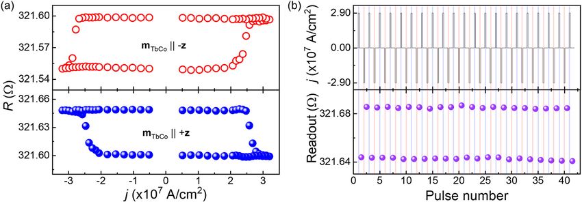
Applied Physics Letters                                                                                              ARTICLE               scitation.org/journal/apl

    (unless stated otherwise). The thickness of this coupling layer was                         switches from up to down. The increase in RH when TbCo switches
    tCo ¼ 0, 0.4, and 1.2 nm, and the thickness of the Pt spacer was varied                     from up to down indicates that the magnetization is dominated by the
    between tPt ¼ 3 nm and 4.5 nm in steps of 0.25 nm for tCo ¼ 0.4 nm.                         Tb sublattice, since RH is mainly due to the Co sublattice.27 The
    All layers were grown in a base pressure of 5  108 mbar and                              reversed sweep signal (red arrows) can be explained using the same
    Ar partial pressure of 2  103 mbar. Two-terminal 2.5-lm-wide                              arguments.
    7.5-lm-long current tracks as well as 5 lm-wide 20-lm-long Hall                                   We then measure the longitudinal resistance (R) during a sweep
    bars were defined on blanket substrates using UV photolithography.                           of Bz [Fig. 1(c)]. For these measurements, we used the two-terminal
    After deposition, the devices were obtained by liftoff as depicted in                       device shown in the bottom panel of Fig. 1(a), fabricated on a separate
    Fig. 1(a). For electrical characterization of the magnetization and for                     chip. Interestingly, we observe a spin-valve-like signal that depends on
    probing the magnetization state during the switching experiments, we                        the relative magnetic orientation of the layers, i.e., two reversal events
    measured the Hall effect and longitudinal resistance using standard                         at low and high fields, which give rise to two distinct resistance levels.
    a.c. current injection methods.26 All experiments were performed in                         We interpret this behavior as the current-in-plane giant magnetoresis-
    ambient conditions.                                                                         tance (GMR) mediated by the Pt spacer. The GMR, however, is about
          We first focus on the first batch of samples with the Pt(4.5 nm)                        0.03%, two orders of magnitude smaller than typical values for TbCo-
    spacer. Figure 1(b) shows the Hall resistance (RH) of the sample with                       based multilayers using a Cu spacer.28,29 This low value of the GMR is
    the Pt(4.5 nm) spacer during an out-of-plane field (Bz) sweep. As evi-                       attributed to the strong spin scatter properties of Pt.30,31 Unlike in the
    dent from the data, two separate magnetization reversal events occur                        conventional GMR measurements, the resistance is high when Co and
    at low field (25 mT) and at high field (750 mT). The low field                               TbCo are parallel to each other and low when they are antiparallel.
    reversal is attributed to the top Co layer as it is within the typical coer-                The high resistance for the parallel state indicates that the GMR
    civity range (10–50 mT) expected of single Pt/Co bilayers. The high                         mainly originates from the interplay between the magnetization of the
    field reversal is attributed to TbCo, which is known to possess large                        top Co layer and the Co magnetic sublattice in the TbCo layer, in
    perpendicular magnetic anisotropy and large coercivity near the mag-                        agreement with previous studies of the GMR in rare-earth transition-
    netic compensation point. This measurement shows that the two                               metal alloys.32–34 Because the magnetization in TbCo is Tb-like, in the
    layers are magnetically decoupled and that their relative magnetic ori-                     parallel (high resistance) configuration, the magnetization of the top
    entation can be preset by an external field. Another interesting aspect                      Co layer is antiparallel to the Co sublattice in the bottom layer, which
    is the sign of the reversal events. Sweeping from þBz to –Bz (blue                          gives rise to the larger resistance. The dominant GMR contribution of
    arrows), RH first decreases at small negative fields, corresponding to                        the Co sublattice in TbCo is reasonable because the spin-polarized
    Co switching from up to down, and then increases when TbCo                                  conduction is mostly dominated by the s-d electrons of Co, whereas

     FIG. 1. (a) Schematics of the devices and multilayer structure used in this study. (b) Hall resistance (RH) and (c) magnetoresistance (R) response of the devices shown in (a)
     during an out-of-plane field (Bz) sweep. (d) Minor loops corresponding to the magnetization reversal of the top Co layer for the two different orientations of TbCo. The thickness
     of the Pt spacer in (b)–(e) is 4.5 nm. See text for further details.

Appl. Phys. Lett. 119, 032406 (2021); doi: 10.1063/5.0055177                                                                                                             119, 032406-2
Published under an exclusive license by AIP Publishing
Applied Physics Letters                                                                                                  ARTICLE               scitation.org/journal/apl

     FIG. 2. (a) Longitudinal resistance (R) measurement of current-induced magnetization reversal of the top Co layer for negative (top panel) and positive (lower panel) magnetization of
     TbCo. We observe reversible switching events starting at around 2.5–3  107 A/cm2 for both TbCo magnetizations and positive/negative current polarity. (b) Consecutive switching of
     the magnetization over 40 pulse cycles (top graph) and corresponding resistance readout (bottom graph). The in-plane field was set to þ200 mT in both sets of measurements. For
     each data point, a train of five pulses of 50 ns duration was sent through the device. The data in each loop were averaged over ten full cycles to enhance the signal to noise ratio.

    the spin-polarized f electrons of Tb have negligible contribution to the                       the switching is fully reproducible for over 40 switching events and no
    conduction.35 The same argument also explains the negative RH                                  drift or partial switching is observed. Moreover, we tested the Bx
    behavior discussed above.                                                                      dependence of jcrit in a wide range of fields and confirmed the behavior
           Figures 1(d) and 1(e) show the minor loops corresponding to the                         expected of SOT-switching. The field dependence of the critical
    reversal of the Co magnetization detected by the Hall effect and resis-                        switching current threshold (jcrit) is plotted in Fig. 3. We observe that
    tance, respectively, for two different orientations of TbCo magnetiza-                         jcrit decreases monotonously with the increasing Bx, as the energy bar-
    tion (mTbCo). In the RH data [Fig. 1(d)], the loops are nearly identical                       rier between the up and down states is effectively reduced. jcrit
    for both positive and negative mTbCo with an offset originating from                           increases more significantly when Bx < 100 mT, which is also expected
    the RH of TbCo. In the resistance data [Fig. 1(e)], however, the loops                         because jcrit is found to diverge as Bx ! 0 (Ref. 36). We were unable to
    have opposite sign for positive and negative mTbCo as the orientation                          extend the measurements to Bx < 50 mT because Joule heating due to
    of mTbCo acts as a reference for the resistance readout. This sign rever-                      the increased j was negatively influencing the readout, and also, partial
    sal will be important to understand the SOT-induced switching data                             switching of TbCo was observed in some cases.
    discussed below.                                                                                      Starting from our proof of concept for a two-terminal spin valve
           Next, we perform current-induced switching experiments on the                           device operated by SOT, we discuss several pathways to enhance the
    resistance tracks. Figure 2(a) shows the resistance during a pulsed-                           signal output. One way to enhance the readout signal is to increase
    current sweep at j < j3.2  107j A/cm2 (estimated by considering the                           the GMR through interface engineering. In Fig. 4(a), we compare
    full stack but excluding the Ti buffer and cap) in the presence of an in-                      the relative resistance change (DR/R) in three different samples with
    plane field Bx 200 mT applied along the current direction as required                          and without a Co insertion layer in between TbCo and Pt. We observe
    for SOT switching.1 Note that for each data point in this and the fol-
    lowing switching measurements (except Fig. 5), we have injected a
    train of five 50-ns-long pulses and averaged the resistance signal for
    1 s. This pulsing/averaging scheme minimizes the signal drift. We
    observe that the magnetization of Co switches between the up and
    down states reversibly at around 2.5–3  107 A/cm2. In reference to
    Fig. 1(e), for the same (opposite) field and current direction, the Co
    magnetization switches from up to down (down to up), which is con-
    sistent with the switching of Pt/Co bilayers dominated by the
    damping-like SOT.1,36 We note that the changes in the resistance
    upon the SOT-induced switching are about half of that reported by
    field-induced switching in Fig. 1(e). This occurs because only the nar-
    row part of the track, where the current density is maximum, switches
    due to the SOT, whereas the field can also switch the wider contact
    regions, which also contributes to the resistance.
           To test the reliability of the device over multiple switching events,
    we injected consecutive pulse trains of opposite polarity with
    Bx ¼ 200 mT. Figure 2(b) shows the pulse sequence (upper panel) and                             FIG. 3. Dependence of critical switching current density (jcrit) as a function of the
    the resistance readout after each pulse (lower panel). We observe that                          static in-plane field (Bx).

Appl. Phys. Lett. 119, 032406 (2021); doi: 10.1063/5.0055177                                                                                                                  119, 032406-3
Published under an exclusive license by AIP Publishing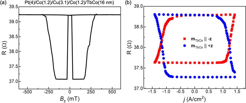
Applied Physics Letters                                                                                                     ARTICLE                scitation.org/journal/apl

     FIG. 4. (a) Effect of Co insertion layer on the magnetoresistance (DR/R). (b) Co minor loops measured using the Hall resistance (RH) for different thickness of the Pt spacer
     (tPt). The data are vertically shifted for clarity. (c) Coercivity of the Co layer (squares, left axis) and coupling strength (circles, right axis) as a function of tPt. We identify three
     regions with strong, weak, and negligible coupling. See text for more details.

    that DR/R increases from 0.02 to 0.05% as the Co thickness increases                                   Finally, we show that by using a Cu spacer and placing the Pt
    from 0 to 1.2 nm. Moreover, we notice that the coercivity of the refer-                          layer on the opposite side of the Co interface relative to TbCo, we
    ence layer is significantly larger when Co is introduced between TbCo                             obtain a strong increase in the GMR while preserving the SOT switch-
    and Pt, which is indicative of an enhanced PMA. This comparison                                  ing capability. Figure 5(a) shows the magnetoresistance of Pt(4)/
    shows that for optimum readout, an insertion layer is beneficial to                               Co(1.2)/Cu(3.1)/Co(1.2)/TbCo(16) during a Bz field sweep. Similar to
    enhance both the interface contribution to the GMR and the PMA of                                the data in Fig. 1(c), we observe a spin valve behavior but with a much
    the reference layer. Further enhancement of the GMR is possible, in                              higher GMR ratio reaching up to 5.9%, which is about two orders of
    principle, by modifying the interface between the top Co layer and Pt.                           magnitude larger compared to the samples with the Pt spacer. The
    However, this approach would affect also the SOT acting on the                                   enhanced GMR is a consequence of the use of a relatively thin Cu
    free layer, because the SOT properties depend sensitively on this                                spacer instead of a thick Pt spacer and the relatively thick Co(1.2 nm)
    interface.37                                                                                     coupling layer attached to TbCo, in view of the conclusions drawn
          Another path to increase the readout signal is to reduce tPt to                            from Fig. 4(a). Figure 5(b) reports the current-induced switching mea-
    maximize the GMR effect.38 However, for the symmetric SOT switch-                                surements on this sample. We achieve switching with moderate cur-
    ing operation (i.e., the same jcrit switches from the parallel to the anti-                      rents of about j  1–1.5  107 A/cm2. We observe that for both
    parallel state and vice versa), the two layers need to be magnetically                           orientations of mTbCo, the switching is partial (70%) compared to
    decoupled. Figure 4(b) shows the Co minor loop data for positive                                 the field-driven switching shown in Fig. 5(a). We assume that the par-
    mTbCo. We observe that the Co hysteresis loops are significantly influ-                            tial switching is related to the inhomogeneous currents flowing in dif-
    enced by tPt. For tPt between 3.0 and 3.5 nm, the hysteresis occurs only                         ferent regions of the Hall bar. These data unambiguously demonstrate
    for positive Bz, meaning that the coupling is antiparallel and the effec-                        a two-terminal spin valve device that is controlled by SOTs with high
    tive coupling field is larger than the coercivity of the top Co layer. The                        readout GMR and moderate write current requirements.
    magnitude of the coupling gradually decreases with the increasing tPt                                  The magnetoresistive reading of spin valves with in-plane or out-
    and the hysteresis loop becomes fully symmetric with respect to                                  of-plane magnetization is a paradigmatic feature of spintronic devi-
    Bz ¼ 0 mT at tPt ¼ 4.5 nm. Figure 4(c) summarizes our findings by                                 ces.41,42 Usually, the magnetization in such structures is controlled by
    showing the coercivity (left axis) and the coupling strength (right axis)                        either an external field or the spin transfer torques due to current
    characterized by the shift of the bistable region delimited by the rever-                        injection perpendicular to the magnetic layers.43,44 Another applica-
    sal events as a function of tPt. We observe that while the coercivity is                         tion of such devices is to study domain wall propagation in the soft
    fairly constant, the coupling strength dramatically changes as a func-                           layer by either fields or spin-transfer torques, while the hard layer
    tion of tPt within the studied range. We delimit three regions: (i) strong                       remains in a single-domain state serving as Refs. 45–47. Only recently,
    coupling where the interlayer coupling is larger than the coercivity of                          there have been efforts to include SOT switching in spin valve devi-
    the minor loop; hence, no bistable region exists at Bz ¼ 0 mT (not suit-                         ces.48,49 However, these studies employed magnetically coupled layers
    able for SOT switching); (ii) weak coupling where the interlayer cou-                            and the Hall effect for reading their magnetic state, which is not suit-
    pling is lower than the coercivity but large enough to prevent SOT from                          able for two-terminal devices. Our measurements take full advantage
    switching; (iii) negligible coupling where the interlayer coupling is barely                     of the spin valve functionalities, adding the versatility of SOT switch-
    noticeable; hence, the minor loop is symmetric around Bz ¼ 0 mT.                                 ing to the simplest magnetoresistive reading of the magnetization.
    Based on these measurements, we conclude that we can only use tPt                                Furthermore, our concept can enhance the functionality of earlier
     4.25 nm, which explains the small GMR of this type of devices. We                              domain wall devices by taking advantage of strong SOTs for efficiently
    speculate that replacing the Pt spacer by a finely tuned light metal/Pt                           nucleating and driving domain walls.7,8 One use of such a device could
    bilayer, where the light metal (e.g., Cr, Ti, or Cu) is inserted between                         be to generate analogue-like resistive signal outputs that depend on
    TbCo and Pt, could generate a large enough SOT to switch the top Co                              the domain wall position. This device concept could find interest in
    layer and increase the GMR readout signal significantly.39,40                                     neuromorphic computing applications.50

Appl. Phys. Lett. 119, 032406 (2021); doi: 10.1063/5.0055177                                                                                                                       119, 032406-4
Published under an exclusive license by AIP Publishing
Applied Physics Letters                                                                                             ARTICLE               scitation.org/journal/apl

     FIG. 5. (a) Magnetoresistance as a function of out-of-plane magnetic field of a spin valve consisting of Pt(4)/Co(1.2)/Cu(3.1)/Co(1.2)/TbCo(16) with a Cu spacer instead of Pt.
     (b) Current-induced switching of the bottom Co layer induced by the SOT generated from the Pt underlayer. The magnetoresistance is measured by a four-point probe on a
     Hall bar structure similar to the one shown in the upper panel of Fig. 1(a). For the switching measurements, we have used pulses of 10 ms and averaged the data over three
     consecutive cycles. The in-plane field Bx was set to þ300 mT.

                                                                                               16
        This work was supported by the Swiss National Science                                     E. Grimaldi, V. Krizakova, G. Sala, F. Yasin, S. Couet, G. Sankar Kar, K.
    Foundation through Grant Nos. 200020_172775 and PZ00P2-                                       Garello, and P. Gambardella, Nat. Nanotechnol. 15(2), 111 (2020).
                                                                                               17
                                                                                                 K. Garello, F. Yasin, H. Hody, S. Couet, L. Souriau, S. H. Sharifi, J. Swerts, R.
    179944.
                                                                                                 Carpenter, S. Rao, W. Kim, J. Wu, K. K. V. Sethu, M. Pak, N. Jossart, D. Crotti,
    DATA AVAILABILITY                                                                            A. Furnemont, and G. S. Kar, “Manufacturable 300 mm platform solution for
                                                                                                 field-free switching SOT-MRAM,” in presented at the 2019 Symposium on
        The data that support the findings of this study are available                            VLSI Circuits (IEEE, 2019), pp. T194–T195.
    from the corresponding author upon reasonable request.                                     18
                                                                                                  B. Dieny, I. L. Prejbeanu, K. Garello, P. Gambardella, P. Freitas, R. Lehndorff, W.
                                                                                                  Raberg, U. Ebels, S. O. Demokritov, J. Akerman, A. Deac, P. Pirro, C. Adelmann,
                                                                                                  A. Anane, A. V. Chumak, A. Hirohata, S. Mangin, S. O. Valenzuela, M. Cengiz
    REFERENCES
                                                                                                  Onbaşlı, M. d’Aquino, G. Prenat, G. Finocchio, L. Lopez-Diaz, R. Chantrell, O.
      1
       I. M. Miron, K. Garello, G. Gaudin, P.-J. Zermatten, M. V. Costache, S. Auffret,           Chubykalo-Fesenko, and P. Bortolotti, Nat. Electron. 3(8), 446 (2020).
       S. Bandiera, B. Rodmacq, A. Schuhl, and P. Gambardella, Nature 476(7359),               19
                                                                                                  G. Prenat, K. Jabeur, P. Vanhauwaert, G. D. Pendina, F. Oboril, R. Bishnoi, M.
       189 (2011).                                                                                Ebrahimi, N. Lamard, O. Boulle, K. Garello, J. Langer, B. Ocker, M. Cyrille, P.
      2
        C. O. Avci, K. Garello, C. Nistor, S. Godey, B. Ballesteros, A. Mugarza, A.               Gambardella, M. Tahoori, and G. Gaudin, IEEE Trans. Multi-Scale Comput.
        Barla, M. Valvidares, E. Pellegrin, A. Ghosh, I. M. Miron, O. Boulle, S. Auffret,         Syst. 2(1), 49 (2016).
        G. Gaudin, and P. Gambardella, Phys. Rev. B 89(21), 214419 (2014).                     20
                                                                                                  Y. Kato, H. Yoda, T. Inokuchi, M. Shimizu, Y. Ohsawa, K. Fujii, M. Yoshiki, S.
      3
        K. Garello, I. M. Miron, C. O. Avci, F. Freimuth, Y. Mokrousov, S. Blugel, S.             Oikawa, S. Shirotori, K. Koi, N. Shimomura, B. Altansargai, H. Sugiyama, and
        Auffret, O. Boulle, G. Gaudin, and P. Gambardella, Nat. Nanotechnol. 8(8),                A. Kurobe, J. Magn. Magn. Mater. 491, 165536 (2019).
        587 (2013).                                                                            21
                                                                                                 V. Krizakova, K. Garello, E. Grimaldi, G. Sankar Kar, and P. Gambardella,
      4
        J. Kim, J. Sinha, M. Hayashi, M. Yamanouchi, S. Fukami, T. Suzuki, S. Mitani,            Appl. Phys. Lett. 116(23), 232406 (2020).
        and H. Ohno, Nat. Mater. 12(3), 240 (2013).                                            22
                                                                                                  C. O. Avci, M. Mann, A. J. Tan, P. Gambardella, and G. S. D. Beach, Appl.
      5
        L. Liu, C.-F. Pai, Y. Li, H. W. Tseng, D. C. Ralph, and R. A. Buhrman, Science            Phys. Lett. 110(20), 203506 (2017).
                                                                                               23
        336(6081), 555 (2012).                                                                    N. Sato, F. Xue, R. M. White, C. Bi, and S. X. Wang, Nat. Electron. 1(9), 508
      6
        C.-F. Pai, L. Liu, Y. Li, H. W. Tseng, D. C. Ralph, and R. A. Buhrman, Appl.              (2018).
                                                                                               24
        Phys. Lett. 101(12), 122404 (2012).                                                       M. N. Baibich, J. M. Broto, A. Fert, F. Nguyen Van Dau, F. Petroff, P.
      7
        S. Emori, U. Bauer, S. M. Ahn, E. Martinez, and G. S. Beach, Nat. Mater. 12(7),           Etienne, G. Creuzet, A. Friederich, and J. Chazelas, Phys. Rev. Lett. 61(21),
        611 (2013).                                                                               2472 (1988).
      8                                                                                        25
        K. S. Ryu, L. Thomas, S. H. Yang, and S. Parkin, Nat. Nanotechnol. 8(7), 527 (2013).      G. Binasch, P. Grunberg, F. Saurenbach, and W. Zinn, Phys. Rev. B 39(7), 4828
      9
        P. P. Haazen, E. Mure, J. H. Franken, R. Lavrijsen, H. J. Swagten, and B.                 (1989).
                                                                                               26
        Koopmans, Nat. Mater. 12(4), 299 (2013).                                                  C. O. Avci, K. Garello, A. Ghosh, M. Gabureac, S. F. Alvarado, and P.
    10
       C. K. Safeer, E. Jue, A. Lopez, L. Buda-Prejbeanu, S. Auffret, S. Pizzini, O.              Gambardella, Nat. Phys. 11(7), 570 (2015).
                                                                                               27
       Boulle, I. M. Miron, and G. Gaudin, Nat. Nanotechnol. 11(2), 143 (2016).                   R. Asomoza, I. A. Campbell, H. Jouve, and R. Meyer, J. Appl. Phys. 48(9), 3829
    11
      A. Manchon, J. Zelezn    y, I. M. Miron, T. Jungwirth, J. Sinova, A. Thiaville, K.         (1977).
                                                                                               28
      Garello, and P. Gambardella, Rev. Mod. Phys. 91(3), 035004 (2019).                          M.-S. Lin, C.-H. Lai, Y.-Y. Liao, Z.-H. Wu, S.-H. Huang, and R.-F. Jiang,
    12
       D. C. Ralph and M. D. Stiles, J. Magn. Magn. Mater. 320(7), 1190 (2008).                   J. Appl. Phys. 99(8), 08T106 (2006).
    13                                                                                         29
       C. Song, R. Zhang, L. Liao, Y. Zhou, X. Zhou, R. Chen, Y. You, X. Chen, and F.             C.-H. Lai, Z.-H. Wu, C.-C. Lin, and P. H. Huang, J. Appl. Phys. 97(10),
       Pan, Prog. Mater. Sci. 118, 100761 (2021).                                                 10C511 (2005).
    14                                                                                         30
       J. Ryu, S. Lee, K.-J. Lee, and B.-G. Park, Adv. Mater. 32(35), 1907148 (2020).             H. Y. T. Nguyen, W. P. Pratt, and J. Bass, J. Magn. Magn. Mater. 361, 30
    15
       M. Cubukcu, O. Boulle, M. Drouard, K. Garello, C. Onur Avci, I. Mihai Miron,               (2014).
                                                                                               31
       J. Langer, B. Ocker, P. Gambardella, and G. Gaudin, Appl. Phys. Lett. 104(4),             F. Garcia, F. Fettar, S. Auffret, B. Rodmacq, and B. Dieny, J. Appl. Phys. 93(10),
       042406 (2014).                                                                            8397 (2003).

Appl. Phys. Lett. 119, 032406 (2021); doi: 10.1063/5.0055177                                                                                                            119, 032406-5
Published under an exclusive license by AIP Publishing
Applied Physics Letters ARTICLE scitation.org/journal/apl
32 42
D. Z. Yang, B. You, X. X. Zhang, T. R. Gao, S. M. Zhou, and J. Du, Phys. Rev. B S. Le Gall, J. Cucchiara, M. Gottwald, C. Berthelot, C. H. Lambert, Y. Henry, D.
74(2), 024411 (2006). Bedau, D. B. Gopman, H. Liu, A. D. Kent, J. Z. Sun, W. Lin, D. Ravelosona,
33
M. Gottwald, M. Hehn, F. Montaigne, D. Lacour, G. Lengaigne, S. Suire, and S. J. A. Katine, E. E. Fullerton, and S. Mangin, Phys. Rev. B 86(1), 014419 (2012).
43
Mangin, J. Appl. Phys. 111(8), 083904 (2012). J. A. Katine, F. J. Albert, R. A. Buhrman, E. B. Myers, and D. C. Ralph, Phys.
34
C. Bellouard, H. D. Rapp, B. George, S. Mangin, G. Marchal, and J. C. Ousset, Rev. Lett. 84(14), 3149 (2000).
44
Phys. Rev. B 53(9), 5082 (1996). D. Bedau, H. Liu, J. J. Bouzaglou, A. D. Kent, J. Z. Sun, J. A. Katine, E. E.
35
Y. Mimura, N. Imamura, and Y. Kushiro, J. Appl. Phys. 47(7), 3371 (1976). Fullerton, and S. Mangin, Appl. Phys. Lett. 96(2), 022514 (2010).
36 45
C. O. Avci, K. Garello, I. M. Miron, G. Gaudin, S. Auffret, O. Boulle, and P. J. Grollier, D. Lacour, V. Cros, A. Hamzic, A. Vaurès, A. Fert, D. Adam, and G.
Gambardella, Appl. Phys. Lett. 100(21), 212404 (2012). Faini, J. Appl. Phys. 92(8), 4825 (2002).
37 46
C. O. Avci, G. S. D. Beach, and P. Gambardella, Phys. Rev. B 100(23), 235454 A. Himeno, T. Ono, S. Nasu, K. Shigeto, K. Mibu, and T. Shinjo, J. Appl. Phys.
(2019). 93(10), 8430 (2003).
38 47
B. Dieny, V. S. Speriosu, S. Metin, S. S. P. Parkin, B. A. Gurney, P. Baumgart, M. Hayashi, L. Thomas, Y. B. Bazaliy, C. Rettner, R. Moriya, X. Jiang, and S. S.
and D. R. Wilhoit, J. Appl. Phys. 69(8), 4774 (1991). P. Parkin, Phys. Rev. Lett. 96(19), 197207 (2006).
39 48
S. N. Kim, J. W. Choi, and S. H. Lim, Sci. Rep. 9(1), 1617 (2019). R. Q. Zhang, J. Su, J. W. Cai, G. Y. Shi, F. Li, L. Y. Liao, F. Pan, and C. Song,
40
S. Ding, A. Ross, D. Go, L. Baldrati, Z. Ren, F. Freimuth, S. Becker, F. Appl. Phys. Lett. 114(9), 092404 (2019).
49
Kammerbauer, J. Yang, G. Jakob, Y. Mokrousov, and M. Kl€aui, Phys. Rev. Lett. G. Y. Shi, C. H. Wan, Y. S. Chang, F. Li, X. J. Zhou, P. X. Zhang, J. W. Cai,
125(17), 177201 (2020). X. F. Han, F. Pan, and C. Song, Phys. Rev. B 95(10), 104435 (2017).
41 50
B. Dieny, V. S. Speriosu, S. S. P. Parkin, B. A. Gurney, D. R. Wilhoit, and D. M. D. Pickett, G. Medeiros-Ribeiro, and R. Stanley Williams, Nat. Mater.
Mauri, Phys. Rev. B 43(1), 1297 (1991). 12(2), 114 (2013).
Appl. Phys. Lett. 119, 032406 (2021); doi: 10.1063/5.0055177 119, 032406-6
Published under an exclusive license by AIP PublishingYou can also read