Addressing Efficiency and Linearity with a Single-Ended Class AB Power Amplifier with optimized Third-Harmonic Termination (part 1) - beam-Verlag
←
→
Page content transcription
If your browser does not render page correctly, please read the page content below
RF & Wireless
Addressing Efficiency and Linearity with a
Single-Ended Class AB Power Amplifier with
optimized Third-Harmonic Termination (part 1)
This application note describes
the design of a single-ended
PA using Class AB “sweet
spots” and an optimized third-
harmonic termination based on
a design flow that encompassed
analysis of the requirements and
initial concepts to the simulation,
fabrication, and measurement of
the built prototype.
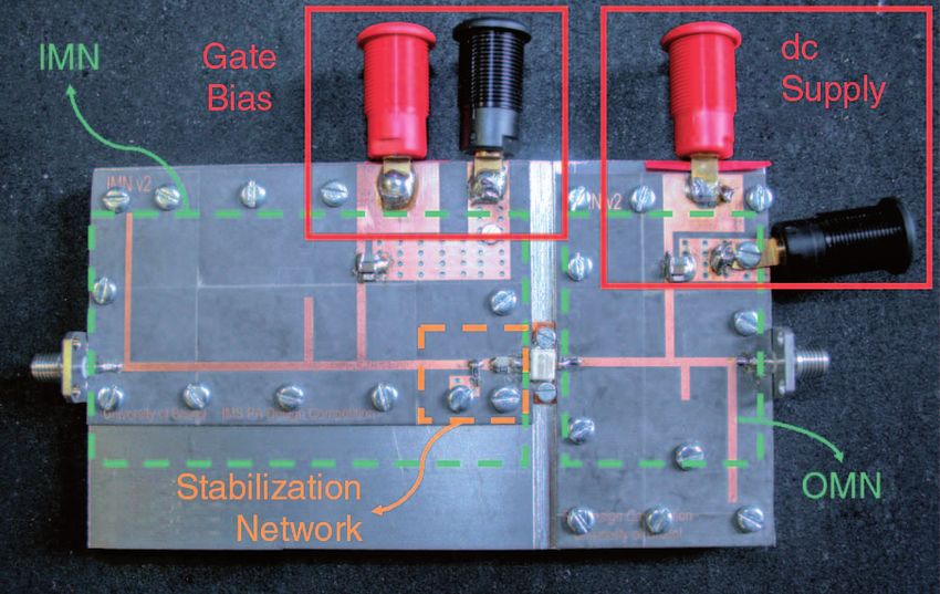
Figure 1: Annotated photograph of completed PA
The single-ended RF power amplifier (PA) her-frequency design. Pout, Pin, and PDC refer
is a standard design approach in the RF to the RF output power of the two tones of
engineer’s tool kit, but high efficiency and interest, the RF input, and DC power sup-
good linearity may only be achieved if the plied, respectively.
harmonic terminations and biasing condi-
tions are carefully examined. The PA design operated at 3 GHz and used
a packaged Wolfspeed [formerly Cree]
The design won first place at the 2016 gallium nitride (GaN) high-electron mobi-
International Microwave Symposium’s High- lity transistor (HEMT). The prototype PA,
Efficiency PA Student Design Competition. shown in Figure 1, achieved a maximum
continuous-wave (CW) output power of
Design Challenge 36.2 dBm and a two-tone PAE of 44 percent
at –30 dBc IMD3, while delivering 34.04
The main challenge of this design was to
dBm of output power.
maximize the overall power-added efficiency
(PAE) of the PA while amplifying a time-
varying envelope signal, without compromi- Problem Formulation
sing the linearity performance. The design At the beginning of a design project, it is
specs required the achievement of the high- necessary to analyze the full range of spe-
est PAE as measured for a two-tone input cifications and survey prior designs that
signal while at the same time ensuring that achieved similar results.
the carrier-to-intermodulation ratio (mea-
sured third-order intermodulation distor- Specifications for the design were:
tion [IMD3] level) was lower than –30 dBc.
• Fewer than 24 dBm (250 mW) of input
A figure of merit (FOM) was calculated from power to reach the point of saturation in
this measurement according to: the presence of a CW signal and produce
Special Thanks to an output power between 36 dBm (4 W)
Paolo Enrico de Falco and 50 dBm (100 W) at saturation
James Birchall and
Laurence Smith for their • Fewer than 22 dBm (158 mW) per tone
Contribution to the application note where the PAE is weighted by the operating to reach the point of saturation in the pre-
National Instruments frequency fr in gigahertz to compensate for sence of a two-equal-tone signal with
ni.com/awr the greater technical challenge in the hig- 5-MHz tone spacing
hf-praxis 4/2018 79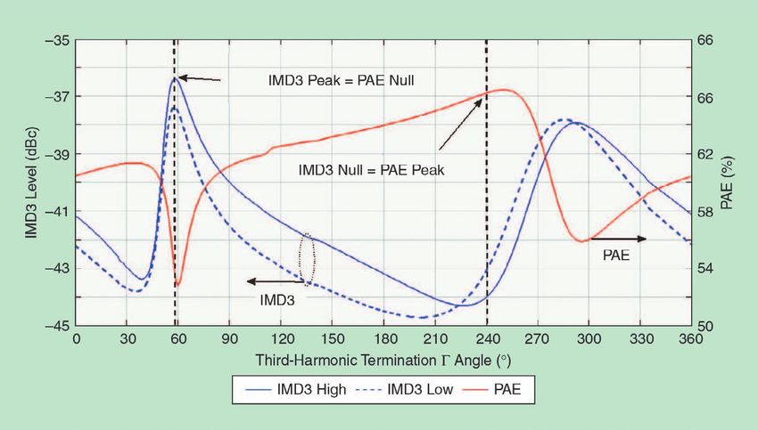
RF & Wireless

Figure 2: The simulated IMD3 versus output power, showing the varying profile and the nulls in IMD3 for different gate bias voltages

• Use a maximum of two DC power sources in only a small FOM improvement. GaN               3-dB backoff range needed to be improved
                                           transistors were chosen for their perfor-        to avoid degrading the average efficiency.
• Operate in the 1–10 GHz frequency range mance at multiple gigahertz frequencies and      Finally, it should be noted that the PAE was
                                           because by operating at the low end of the       measured at -30 dBc IMD3 rather than at
The main constraint placed on the design
                                           36–50 dBm range, their efficiency could be       saturation.
was the large-signal CW gain, which had
                                           further enhanced.
to be above 12 dB at saturation to achieve                                                  For conventional amplifiers, the PAE was
the minimum output power of 36 dBm. For A two-tone signal with 5-MHz frequency              seen to increase monotonically until heavy
the operating frequency, values between 3 spacing was used to evaluate the design.          compression occurred, so, to maximize the
and 5 GHz were considered because, due Closely spaced two-tone signals have a               measured PAE, it was helpful to maintain
to the frequency dependence of the FOM variable time-domain envelope with a 3-dB            a linear power transfer characteristic until
in Equation 1, a higher value would result peak-to-average power ratio, so PAE over a       saturation. A trade off between linearity

Figure 3: The simulated IMD3 and PAE versus the third-harmonic reflection coefficient angle, illustrating the matching peaks and nulls
of the two profiles

80                                                                                                                   hf-praxis 4/2018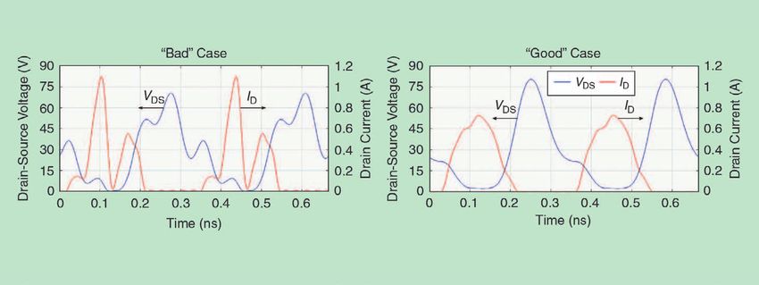
RF & Wireless

Figure 4: The intrinsic drain-source voltage and drain current waveforms for a) “bad” and b) “good” third-harmonic impedance
termination

and efficiency was, therefore, inevitable,        solution, a single stage design has several      However, little investigation has been done
and a good balance was crucial to achieve         practical advantages, including a single         in considering the effect of third-harmonic
the desired FOM.                                  active device, less extensive biasing and        termination on linearity, which is particu-
                                                  matching circuitry, simplicity for imple-        larly significant in Class AB PAs.
Design Solution                                   menting and iterating, and low cost and
                                                  form factor.                                     Figure 3 shows the result of a harmonic
The linear DPA architecture has been shown
in other designs to adapt well to the design      Moreover, a strong understanding and cha-        balance (HB) CW simulation sweeping
requirements providing remarkable results         racterization of a linear, single-ended Class    the third-harmonic impedance at a constant
due to a number of features that comple-          AB amplifier provides a good foundation          input drive level for a Class AB PA, with
ment the specifications. Broadly speaking,        for the design of the main amplifier stage       fundamental and second-harmonic impe-
the active load pull of the main amplifier        in a DPA or other load modulation-based          dances optimized for PAE. As the figure
by the peaking amplifier ensures improved         architectures.                                   indicates, the effect on PAE and IMD3 is
efficiency in the back off region. Through                                                         notable, with the null in IMD3 correspon-
                                                  In Class AB PAs, the nonlinearities intro-       ding to a peak in PAE and vice versa.
the appropriate choice of biasing - Class AB
                                                  duced by the output current waveform’s
for the main and Class C for the peaking -
                                                  truncation (which is, itself, a function of
the compressive and expansive nature of the                                                        This is due to an appropriate third-harmo-
                                                  input drive level and bias) can compensate
transfer characteristics of the two branches                                                       nic short, which promotes a correct sha-
                                                  for the weak nonlinearities introduced by
can be exploited to compensate for one ano-                                                        ping of the voltage waveform and reduces
                                                  the transistor to produce favorable line-
ther, thereby suppressing IMD3 and enabling                                                        the overlap in current and voltage at the
                                                  arity performance at a given drive level.
linear operation up until saturation.                                                              current generator (CG) plane of the tran-
                                                  Specifically, for deep Class AB conduc-
Improving on previous design performance          tion angles, the current waveform trunca-        sistor. This is further shown in Figure 4,
was thus no easy task. One option considered      tion causes a compression of its fundamen-       which illustrates the intrinsic voltage and
was to increase the degree of load modula-        tal frequency component with increasing          current waveforms for different cases of
tion compared to the previous linear DPAs,        drive level, which can compensate for the        third-harmonic termination, which will be
which could boost the efficiency at back          expansive characteristic exhibited by real-      further explained in the following section.
off. However, this would only be obtained         world transistors in the turn-on region. For
if the linearity of the main amplifier’s trans-   two-tone signals, this translates into local     The designer chose NI AWR software, speci-
fer characteristic could also be improved,        minima, or “nulls,” in the IMD3 profile at       fically Microwave Office circuit design soft-
allowing for the peaking stage to turn on         certain points in the amplifier’s response,      ware for all circuit simulations and focused
when the main amplifier has maximum (or           as shown in Figure 2. (In the graphs in the      on finding accurate models for the devices
close to maximum) voltage swing. Ulti-            figures that follow, “high” and “low” refer      and lumped elements used. Following an
mately, the designer decided to focus on          to the IMD3 measured for the intermodu-          extensive survey of packaged GaN HEMT
extending the linearity of a single-ended PA      lated components above and below the two         devices, the Cree CGH40006P was selected
through exploiting specific operating con-        carrier tones, respectively.)                    based on its highly accurate and verified
dition values for Class AB gate bias values                                                        large-signal model and its power and gain-
that are found to improve the linearity of        To further improve efficiency and increase
                                                  the linear dynamic range of the amplifier, the   frequency performance. The microstrip cir-
the PA’s power transfer characteristic, while
                                                  appropriate impedance terminations must          cuitry was modeled using AXIEM 3D planar
also tuning the third harmonic termination.
                                                  also be considered. Prior work has mostly        electromagnetic (EM) simulator and Murata
Despite having drawbacks in terms of per-         addressed the impact of the second-har-          high-precision ceramic capacitors were cho-
formance when compared to a linear DPA            monic impedance termination on linearity.        sen for their accurate parasitic model. ◄

hf-praxis 4/2018                                                                                                                            81
You can also read