Analysis of Bipolar Integrated Circuit Degradation Mechanisms Against Combined TID-DD Effects
←
→
Page content transcription
If your browser does not render page correctly, please read the page content below
IEEE TRANSACTIONS ON NUCLEAR SCIENCE, VOL. 68, NO. 8, AUGUST 2021                                                                                     1585

  Analysis of Bipolar Integrated Circuit Degradation
  Mechanisms Against Combined TID–DD Effects
          Rudy Ferraro , Rubén García Alía , Member, IEEE, Salvatore Danzeca, and Alessandro Masi

   Abstract— Integrated circuits sensitive to both total ionizing            that can lead to completely different degradation rates as it has
dose (TID) and displacement damage (DD) effects can exhibit                  been demonstrated in our previous work [3] with a bipolar IC
degradation profiles resulting from a combination of degradation             current source exposed to different ratios.
mechanisms induced by both effects. This work presents circuit
simulations based on experimental data to explain degradation                   While no qualification standards exist for ICs exhibiting
mechanisms induced by combined TID and DD effects on a                       combined TID–DD internal circuit effects, a similar phenom-
bipolar IC current source. First, the effect of the degradation              enon has been intensively studied in the literature, which is
of each internal transistor on the circuit’s response is evaluated           the qualification of circuits exhibiting circuit effects induced
by applying electrical parametric changes. Then simulations                  by ELDRS. For this effect, it has been shown that for most
are performed from different degradation scenarios based on
observed circuit behaviors to reproduce the different TID, DD,               of the devices the total circuit degradation could be related
and combined TID–DD responses. These simulations show that a                 to the degradation of a single transistor in the circuit such as
synergistic interaction between a current leakage induced by DD              in [4] and [5]. However, this is not systematically true, and
on a transistor located in the bandgap reference part with the               as it is the case for TID and DD, it has also been shown that
gain degradation of a current mirror induced by both TID and                 the different internal transistors of an IC can exhibit different
DD appears to be responsible for the combined TID–DD response.
It is also shown that the circuit degradation rate depends on the            sensitivities to the ELDRS effect and therefore a device can
DDD/TID rate ratios encountered during the exposition.                       present completely different degradation profiles depending on
                                                                             the TID dose rate [6]. Therefore, the proposed methodology to
   Index Terms— Displacement damage (DD), IC radiation
response, nonionizing energy loss, particle accelerator, total               qualify components against this effect is to identify the worst
ionizing dose (TID).                                                         case responses by irradiation at very LDRs [7], [8], assessing
                                                                             the LDR degradation or dependence of the device.
                      I. I NTRODUCTION                                          In our previous work [3], the same approach was followed
                                                                             and a similar methodology to qualify components against
T    HE total degradation response of integrated circuits
     exposed to radiation results from the degradation of
all their internal transistors [1], [2] independently of the
                                                                             combined TID–DD based on the assessment of the dependence
                                                                             between degradation and failure rate with the DD over TID
technology used (CMOS, BiCMOS, or bipolar). While CMOS                       rate ratio. An example of the application of this methodology
technology is only affected by total ionizing dose (TID) and                 was proposed with a bipolar IC whose observed changes
not by displacement damage (DD) dose (DDD) (for standard                     in degradation profiles with different DDD/TID ratios were
DDD that COTS are exposed to), the bipolar technology, and                   assumed to be due to degradation interactions at the internal
thus the BiCMOS one as well, can be affected by both TID                     circuit level.
and DD, and even enhanced low dose rate (LDR) sensitivity                       This article aims to propose a deeper analysis of the
(ELDRS) effect.                                                              behavior of this component through simulations based on
   This interaction of the radiation effects at the internal                 experimental data to understand in detail how in this com-
circuit level can make challenging the qualification of devices              ponent the different degradation mechanisms can combine
exposed to environments inducing both effects such as the                    and lead to the observed responses. First, the device response
ones present in high-energy accelerators, nuclear reactors,                  against TID and DD will be presented. Then, the simulation
or deep space missions. At CERN, the qualification of ICs                    model is introduced and the impact of the degradation of each
against such combined effects is a major concern for radiation               internal component on the circuit response is demonstrated.
hardness assurance (RHA). The large hadron collider (LHC)                    Then, based on experimental assumptions two circuit degrada-
environments present a wide range of DDD/TID rate ratios                     tion profiles are defined to simulate the device response against
                                                                             TID and DD individually. Finally, it is demonstrated how the
  Manuscript received March 22, 2021; revised May 3, 2021; accepted          impact of the DD on the circuit can be enhanced by the TID
May 12, 2021. Date of publication May 21, 2021; date of current version      in a nonlinear way.
August 16, 2021. This work was supported by the European Union’s Horizon
2020 Research and Innovation Programme under Grant Agreement 654168.
  The authors are with the European Organization for Nuclear Research                                 II. C IRCUIT M ODEL
(CERN), 1211 Geneva, Switzerland (e-mail: rudy.ferraro@cern.ch).                The device used for this study is the LM334, which
  Color versions of one or more figures in this article are available at
https://doi.org/10.1109/TNS.2021.3082646.                                    is a proportional-to-absolute temperature (PTAT) adjustable
  Digital Object Identifier 10.1109/TNS.2021.3082646                         current source. No simulation model is provided by the
     This work is licensed under a Creative Commons Attribution 4.0 License. For more information, see https://creativecommons.org/licenses/by/4.0/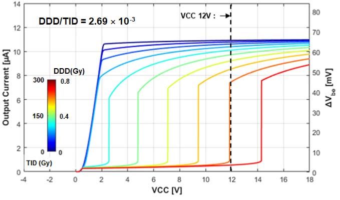
1586                                                                        IEEE TRANSACTIONS ON NUCLEAR SCIENCE, VOL. 68, NO. 8, AUGUST 2021

                                                                            Fig. 2. Output current value of LM334 as a function of V+ to V− voltage for
                                                                            different values of set resistances from datasheet (left) and SPICE simulation
                                                                            (right).

                                                                                                           TABLE I
                                                                                             T RANSISTOR SPICE PARAMETERS U SED
                                                                                              FOR THE LM334 S IMULATION M ODEL

Fig. 1.     Simplified internal circuit of LM334 with the different parts
underlined.

manufacturer, and therefore the SPICE simulation circuit was
developed according to the analysis of the internal circuitry
shown in Fig. 1 and the component characteristics described                 current mirror design to provide several times the current IC1 .
in the datasheet [9].                                                       In the datasheet, the ratio of ISET to I E1 is equal to 17, which
   The circuit is composed of three different parts: a modified             implies that IC6 is 16 times higher than I E1 , and therefore
Brokaw bandgap circuit, a negative feedback circuit, and a                  transistor Q6 is composed of 16 transistors in parallel.
current mirror part. The principle of the circuit is to provide the            With the correct estimation of the numbers of transistors
fixed reference voltage called V BE on the resistor R1 inde-               in parallel composing Q1 and Q6, it is possible to build
pendently of the resistor value. Therefore, the current flowing             a SPICE model with a quite realistic behavior as can be
through the load resistor is proportional to the R1 resistor. This          seen from Fig. 2 comparing the simulated output current with
voltage is provided by the Brokaw bandgap circuit and is equal              the datasheet ones for different values of R1. As previously
to the difference in base–emitter voltage of the transistors                mentioned, no information about the internal transistors is
Q1 and Q2, which is induced by the fact that Q1 is composed                 provided by the manufacturer, and therefore the transistor
of several transistors in parallel. The equation ruling the circuit         parameters used in the simulation are arbitrary and have
is the following:                                                           been obtained combining educated guesses and fine-tuning to

                                 kT       n I c1     kT                     reproduce the different device electrical characteristics. The
     V BE = VBE1 − VBE2 =           ln            =    ln(n) (1)           parameters used in the model are shown in Table I, where
                                  q        Ic2        q
                                                                            I s is the transport saturation current, Hfe the forward active
where k is the Boltzmann’s constant, q is the charge of an
                                                                            current, CJC the base–collector zero-bias junction capacitance,
electron, T is the absolute temperature in K, n is the number
                                                                            CJE the base–emitter zero-bias junction capacitance, VAF the
of transistors Q1 in parallel, Ic1 is the collector current of              forward early voltage, and TF the ideal forward transit time.
transistor Q1, and Ic2 is the collector current of transistor Q2.
                                                                            All the others are the default ones of the SPICE transistor
Therefore, since the transistors Q1 and Q2 are identical if
                                                                            models.
IC2 is kept equal to IC1 , V BE is linearly dependent on the
                                                                               Any degradation of these three main parts will impact the
temperature. For a temperature equal to 25 ◦ C, kT /q is equal
                                                                            circuit’s response.
to 25.7 mV. In the datasheet, V BE is equal to 64 mV, and
therefore the number of transistors Q1 in parallel is 12.
   Then, the role of the negative feedback is to keep the two                                   III. R ADIATION R ESPONSES
collector currents equal independently of the voltage supply                   To gather more information on the internal degradation
or the value of the resistor R1 by setting the necessary base               mechanisms, new irradiations against TID have been per-
current of Q4 and Q5.                                                       formed besides the one presented in our previous work [3].
   Then, the fixed current provided by the circuit in the load              During these irradiations, not only the output current was mon-
resistor is equal to                                                        itored but also the output current as a function of the voltage
                                                                            supply characteristic at different irradiation steps. The irradia-
             ISET = I E1 + IC6 + I E3 ≈ I E1 + IC6 .                 (2)
                                                                            tion conditions during these additional tests together with the
  The current I E3 is equal to the base currents of Q4, Q5,                 ones previously performed are summarized in Table II.
and Q6; it is then negligible compared with the other collector                For each test, at least five devices were tested. Three
currents for h feQ4−6  1. On the other hand, Q6 is a multiplier            types of tests were conducted, TID tests, DD tests, and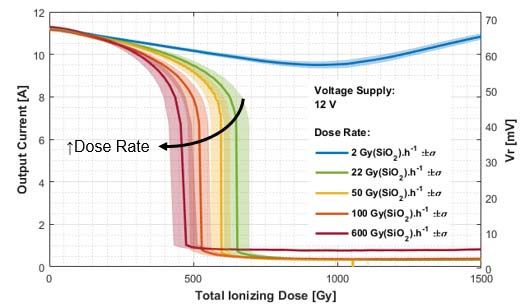
FERRARO et al.: ANALYSIS OF BIPOLAR INTEGRATED CIRCUIT DEGRADATION MECHANISMS                                                      1587

                            TABLE II                                facilities with strong gamma contributions allow reaching the
                    I RRADIATION C ONDITIONS                        10−3 range. This last possibility was tested with this device,
                                                                    where irradiations have been performed at the Triga Mark II
                                                                    research nuclear reactor of the Jožef Stefan Institute (JSI).
                                                                    In this reactor, the gamma contribution can be quite high
                                                                    depending on the test position selected; during our experiment,
                                                                    the DDD/TID ratio was at 3.09 × 10⁻³ , which is two orders
                                                                    of magnitude lower than the PROSPERO reactor.
                                                                       Also, irradiations have been performed at PSI with
                                                                    a 200-MeV proton beam, but as it is often the case for this kind
                                                                    of facility, the ionizing dose rate was quite high, 500 Gy.h−1 ,
                                                                    as shown in Table II.
                                                                       In the case of CERN, another solution can be used, which is
                                                                    using different kinds of mixed fields provided by the CERN
                                                                    high-energy accelerator mixed field (CHARM) facility [16].
                                                                    The CHARM mixed radiation field is composed of the sec-
                                                                    ondary particles resulting from the collision of a 24-GeV
                                                                    proton beam extracted from the proton synchrotron (PS) on
                                                                    cylindrical copper or aluminum targets in the experimental
combined TID–DD tests. Pure TID responses were obtained             area. Then, using different test locations, targets, and shielding,
with gamma irradiation performed in the CC60 facility of            the facility can achieve a wide range of DDD/TID ratios as
CERN with a cobalt 60 source [10]. It has to be noted               shown in a previous work [3]. Three different irradiations
that gamma rays also induce DD, but for the TID levels              at different ratios indicated in Table II were performed to
considered for COTS components and the one reached in this          study the impact of combined TID–DD effects on the circuit
study, this contribution is considered negligible. Considering      response at different DDD/TID ratios.
the NIEL values given in [11] and [12] that are around                 The most important factor to be considered here is the
1.1 × 10⁻⁷ MeV.cm2 /g and considering a dose deposited by           ionizing dose rate. It is assumed that no DDD dependence
photons of 3 × 10⁻² MeV.cm2 /g for standard average energy          is expected within the fluxes used during those tests; however,
of 1.25 MeV, this gives a DDD/TID ratio of 3.57 × 10⁻⁶ as           bipolar transistors can show significant sensitivity to dose-rate
shown in Table II. This means that for the maximum ionizing         effects, and therefore dose-rate effects have to be carefully
dose reached in this work of 2.5 kGy, the devices are exposed       considered to compare the different irradiation tests.
to a DDD of 8.5 mGy, which is considered too low to induce
any significant degradation.
   The DD response was obtained by exposing devices at the          A. Total Ionizing Dose Responses
PROSPERO neutron irradiation facility of the Commissariat à            To investigate possible dose-rate effects and to allow a direct
l’Energie atomique et aux énergies Alternatives (CEA) [13].         comparison with the combined TID–DD irradiations, a set of
As for the CC60 facility, in the PROSPERO facility the devices      devices has been irradiated to different ionizing dose rates,
are also exposed to a small fraction of TID due to the gamma        ranging from 2 to 600 Gy(SiO2 ).h−1 . Based on the circuit
rays also generated by the nuclear reactor. The DDD/TID ratio       radiation responses, the dose rates have been separated into
measured during the experiment was 3.09×10⁻¹, which means           two groups; LDR, which corresponds to the lowest ionizing
that for the DDD of 4 Gy, the devices were exposed to only          dose rate used, 2 Gy(SiO2 ).h−1 , and high dose rates (HDRs),
13 Gy, and therefore it is assumed that the level of interactions   which corresponds to ionizing dose rates from 22 up to
between TID and DD should be very low.                              600 Gy(SiO2 ).h−1 . The device responses corresponding to
   Then, two possibilities exist to test in different DDD/TID       these two groups are presented in the following sections.
ratio conditions during the combined TID–DD irradiations.              1) Low Dose Rate: The evolution of the output current
The first consists of using monoenergetic charged particle          of five devices with an LDR of 2 Gy(SiO2 ).h−1 is shown
beams. Different ratios can be reached using different par-         in Fig. 3. As visible, at this rate, the devices seem to
ticles or different energies of the same particle. For instance,    suffer from two different degradation mechanisms, the first
at CERN for radiation qualification purposes, the proton            one inducing a slow decrease of the output current up to
irradiation facility (PIF) of the Paul Scherrer Institute (PSI)     1 kGy(SiO2 ) and a second one increasing it back even further
is widely used. It provides proton energies ranging from            the initial value. One can note that during this test the devices
30 MeV up to 220 MeV, which corresponds to DDD/TID ratios           have shown a relatively low variability of responses. The
ranging from 3 to 6 × 10⁻⁴ , which is rather low compared           evolution of the output current as a function of the voltage
with levels that have to be reached to be representative            supply characteristics for a single device for both before and
of the LHC environments [3], which range from 10−4 up               after 1 kGy(SiO2 ) is shown in Fig. 4. As visible, the global
to 10−2 . Mixing different types of particles and energies would    shape of the characteristic did not change significantly during
allow achieving values over the whole range, for instance,          the irradiation but only the saturation current level changed,
electrons allow to obtain ratios in the 10−5 range while neutron    decreasing up to 1 kGy(SiO2 ) and then increasing after.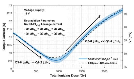
1588                                                                          IEEE TRANSACTIONS ON NUCLEAR SCIENCE, VOL. 68, NO. 8, AUGUST 2021

                                                                              Fig. 5. Output current response of LM334 supplied in 12 V at several HDRs
Fig. 3.   Output current response of five LM334 components biased to          with the LDR response in comparison.
provide about 10 mA and supplied in 12 V up to a TID of 2.5 kGy(SiO2 ) at
2 Gy(SiO2 ) · h−1 .

                                                                              Fig. 6. Evolution of current output as a function of voltage supply against
                                                                              TID up at 100 Gy(SiO2 ) · h−1 .

                                                                              effect on the circuit. This kind of phenomenon can happen
                                                                              if the transistor or group of transistors responsible for the
                                                                              first degradation mode reach saturation of their current gain
                                                                              degradation, as it happens at such high cumulated doses,
                                                                              before the second group of transistors responsible for the
                                                                              second degradation mode.
                                                                                 At this stage, already only with TID, at a LDR, different
                                                                              degradation mechanisms with opposite effects seem to occur.
                                                                              The question arises as to how these two mechanisms can
                                                                              evolve when exposed to DD in addition to TID. If the
                                                                              transistors responsible for these degradation mechanisms have
                                                                              different sensitivities to DD, the circuit might exhibit com-
                                                                              pletely different behavior depending on the DDEF/TID ratio.
                                                                                 2) High Dose Rate: Concerning the HDR responses,
                                                                              the degradation profile is different than the LDR response.
Fig. 4. Evolution of current output as a function of voltage supply against   As visible in Fig. 5 for different dose rates, the current
TID up to 1 kGy(SiO2 ) (top) and from 1 up to 2.5 kGy(SiO2 ) (bottom).
                                                                              decreases monotonically at a higher rate before suddenly
                                                                              dropping to almost 0. The higher the dose rate, the higher
   It seems that two degradation mechanisms impact the                        the degradation rate.
LDR circuit response with the mechanism responsible for                          Then, the evolution of the Iout = f(Vcc) characteristic for
the decrease being dominant below 1 kGy(SiO2 ). It can be                     a dose of 100 Gy(SiO2 ).h−1 is visible in Fig. 6. From this
assumed that the degradation observed is a combination of                     figure it is possible to see that in addition to the decrease in
gain degradations occurring in different parts of the internal                the saturation current, the minimum startup voltage (referred
circuit as it has been observed for other circuits with similar               hereafter as VSTART ) necessary to activate the circuit has
responses [1], [2]. Assuming that the degradation of the circuit              rapidly increased with the dose, causing the sudden drop
is probably due to the degradation of the current gain of its                 visible in Fig. 5. This kind of behavior is usually due to
internal transistors, this could be the result of the degradation             the degradation of the startup circuit of the device. It has
of two different transistors or group of transistors with opposed             already been observed on similar devices such as voltage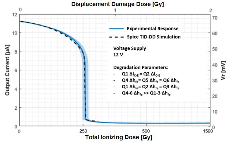
FERRARO et al.: ANALYSIS OF BIPOLAR INTEGRATED CIRCUIT DEGRADATION MECHANISMS                                                    1589

regulators, which use also bandgap-based circuits like in [15],
for instance, where the current gain degradation of one of the
input PNP transistors was leading to the increase in the startup
voltage required to enable the regulation.
   It is curious that this effect does not appear at LDRs and
seems to be enhanced with higher dose rates. If this effect was
due to a current gain degradation, it should either be higher
at LDRs if the device is sensitive to ELDRS or at least not be
so much lower. This could indicate that this effect is not due
to a gain degradation but rather to a current leakage increase.
Similar behavior has been observed in the LM117 [2] where
an increase in the collector to emitter (IC−E ) current leakage
of one of the transistors of the bandgap circuit was visible at     Fig. 7.   LM334 DD responses as a function of DDD/TID ratios from
HDRs and not at LDRs.                                               experiments performed in the CHARM and JSI Facilities.

                                                                    rate was very low, it can be assumed that the current leakage
B. Combined TID–DD Responses
                                                                    is in this case induced by DDs.
   A first observation that can be made regarding the pre-             Then the second observation is the fact that while increasing
viously discussed TID data is that the higher degradation           the ratio of TID during the different combined TID–DD
observed in the past with protons was certainly due to the          irradiations, the global degradation shape is similar, but with
difference in the dose rate between the gamma and the               a higher degradation rate. Therefore, the degradation mecha-
proton experiment. Indeed, it can be seen that the degradation      nisms down to the ratio of 2.69 × 10⁻³ is the same as for the
response obtained with the gamma source at an ionizing              practically pure DD test.
dose rate of 620 Gy(SiO2 ).h−1 is practically the same as the          Based on these different assumptions, different types of
proton response shown in [3] where the current drops suddenly       degradation were applied at the transistor level to see their
around a TID of 500 Gy(SiO2 ). This indicates that at this high     impact at the circuit level, and from these individual degrada-
ionizing dose rate, the TID degradation mechanisms seem to          tions, different circuit degradation scenarios have been simu-
dominate over the DD ones at this DDD/TID ratio. However,           lated to explain the observed degradation curves.
such a high ionizing dose rate is not representative of the
LHC ones, and thus the proton response might overestimate                            IV. C IRCUIT S IMULATIONS
the degradation rate. For this reason, these proton data are not
                                                                       To simulate the radiation effects of BJT on SPICE, it is
further considered for this study.
                                                                    possible to modify their electric parameters, commonly the
   Then, the different combined TID–DD irradiation responses
                                                                    current gain (Hfe ) and the current leakages. However, the
showed in comparison to the individual TID and DDD
                                                                    response of the circuit also depends on other parameters such
responses scale to the DDD/TID ratios together with their
                                                                    as the saturation currents and Early voltages. In our case, none
intrinsic device-to-device variabilities were also discussed
                                                                    of these parameters is known and arbitrary values giving the
in [3]. On the other hand, to discuss the data from another per-
                                                                    same circuit response as in the datasheet have been selected.
spective, the different combined irradiation responses obtained
                                                                    The variations in these parameters to simulate radiation effects
with different ratios are shown all together in Fig. 7 as a
                                                                    are also arbitrary. However, the main objective of this work is
function of DDD. Since in this figure each curve corresponds
                                                                    more to understand how the different mechanisms can interact
to a different DDD/TID ratio, no TID axis is shown since the
                                                                    with each other and lead to the observed circuit degradation
devices are exposed to different amounts of TID for the same
                                                                    responses rather than identifying the exact amount of internal
DDD. The choice of representing them as a function of the
                                                                    degradation.
DDD dose instead of the TID is motivated by the outcome
                                                                       The simulations were performed in two different steps; in
of the circuit simulation that will be described in detail in
                                                                    the first one, parametric changes are applied to the transistors
the following section, showing that the primary degradation
                                                                    individually to understand their impact on the circuit output,
mechanisms seem to be induced by DDs. Therefore, this
                                                                    and then different scenarios of degradation combinations were
figure is further discussed in the combined TID–DD simulation
                                                                    tested to reproduce the observed circuit radiation responses.
section of this article.
   However, two important observations can be made at this
stage from these responses. The first one is the fact that the      A. Current Gain Degradations
response obtained in the PROSPERO nuclear reactor where the            The first type of degradation applied is the current gain Hfe
DDD/TID ratio was at 3.1 × 10⁻¹ is very similar to the one          decrease or said differently, the increase in the base current.
observed with HDR where the increase in the startup voltage         Two different impacts at the circuit level can be observed.
leading to this sharp decrease in the output current is assumed     With this type of degradation, two different effects on the
to be caused by a current leakage. Considering this assumption      circuit response were observed, the increase or the decrease
as correct, since during this test the cumulated TID was only       in the bandgap voltage reference depending on the transistor
13 Gy during this irradiation and the fact that the ionizing dose   impacted.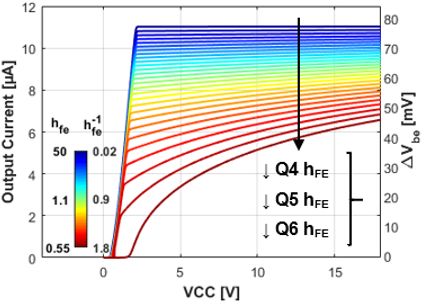
1590                                                                  IEEE TRANSACTIONS ON NUCLEAR SCIENCE, VOL. 68, NO. 8, AUGUST 2021

   1) Bandgap Reference Voltage Decrease: The decrease in
the bandgap reference voltage, which in return controls the
fixed output current, can be induced by the degradation of
any of the transistor Q3, Q4, Q5, or Q6.
   Focusing first on the effect of the decrease in the gain of
Q4, Q5, and Q6, their degradation will lead to the decrease in
their collector current for the same base current. This will
decrease the current flowing through R1, and thus V BE .
To compensate for this effect, the feedback transistor Q3 will
increase proportionally its collector current, and thus the base
current of Q4–6, to maintain the same output current satisfying
IC1 = IC2 and V BE = 0.64 mV. However, at the same
time that Q3 increases its collector current, it increases its
base current, which drains the collector current of Q4 feeding
the current IC2 of the Brokaw cell. Therefore, while Q3
compensates the excess current gain of Q4–6, it also decreases
the current IC2 . Therefore, when the increased base current of
Q3 is no more negligible compared with IC2 , it is not possible
anymore for the circuit to keep the branches of the Brokaw cell
balanced. Then, according to (1) if IC2 becomes lower than
IC1 , the ratio of the currents becomes lower than 1 and then
V BE decreases. Similarly, the decrease in the current gain of
the feedback transistor Q3 itself will lead to the increase in
its base current, which will lead to the same decrease in Ic2 .
   The effect of the decrease in the current gain of each
of these transistors on the Iout = f(Vcc) characteristic and
the corresponding evolution of V BE as a function of the
reciprocal of the gain are shown in Fig. 8. These values have         Fig. 8. Degradation impact of transistors Q4, Q5, Q6, and Q4–6 on LM334
                                                                      V B E = f(VCC) characteristics (top) and on V B E change (bottom).
been calculated considering an arbitrary initial current gain
of 50 for each of them. It can also be seen that Q6 being             B. Current Leakage Increase
composed of 16 transistors in parallel has a much greater
                                                                         It has been shown in [2] and [14] that the transistors Q1 and
impact than Q4 and Q5 for the same degradation. It has to
                                                                      Q2 of the Brokaw circuit could suffer from the collector to the
be noted that the impact of the degradation of Q4–6 is greatly
                                                                      emitter (C–E) with TID at HDR. In the LM334, the feedback
dependent on the initial current gain of Q3. For a high initial
                                                                      reaction is connected to Q2 and thus can be affected by a
Q3 gain, a larger degradation of Q4–6 is necessary to have
                                                                      current leakage on Q2.
the same effect.
                                                                         To simulate the C–E leakage parts, high resistances are
   2) Bandgap Reference Voltage Increase: On the other hand,          placed between the collector and emitter terminals of Q1 and
decreasing the current gain of the transistors Q1 and Q2 of the       Q2 in the same way as in [15]. By decreasing their values,
Brokaw cell will lead to the increase in the voltage reference.       it is possible to simulate the increase in current leakage
Starting with Q1, the main effect of its gain degradation is to       due to radiation. The effect of Q2 IC−E increase is shown
affect its ability to mirror the current I2 . The current of Q1 can   in Fig. 10. It can be seen that the current leakage induces
be described with the following equation neglecting the Early         an increase in the startup voltage VSTART . Additionally, the
effect:                                                               minimum base current required by Q3 depends on the collector
                                1                                     current it has to provide to start the Brokaw cell circuitry. This
                      I2 =                · I1 .               (3)    minimum current will be proportional to the current gain of the
                             1 + h fe2
                                     C2                               transistors Q4–6 and more particularly to the one of Q6 since
                                                                      it requires much more current. Consequently, the decrease in
   Before irradiation, the first term is practically equal to 1 due   the gain of Q6 will enhance the effect of the current leakage
to the high gain value. While the radiations decrease the             of Q2. This enhancement can be seen in Fig. 10 where the
gain, this term decreases, and the current I2 becomes lower           change in the startup voltage is shown as a function of the
than I1 . Therefore, in (1) since I2 decreases, the ratio of I1       current leakage for several Q6 current gain values.
over I2 becomes higher than 1, which increases the voltage
reference V BE .
                                                                      C. TID Circuit Response
   A similar effect occurs with the degradation of Q2. While its
gain decreases, its collector current is also decreases, leading         The most likely scenario explaining the observed degrada-
to the same effect as the degradation of Q1. The impact of            tion curves is that in the first place, the combined degradation
these two mechanisms on the V BE degradation is also shown           rate of Q3–6 dominates over the degradation rate of Q1 and
in Fig. 9.                                                            Q2, leading to the decrease in the bandgap voltage. Then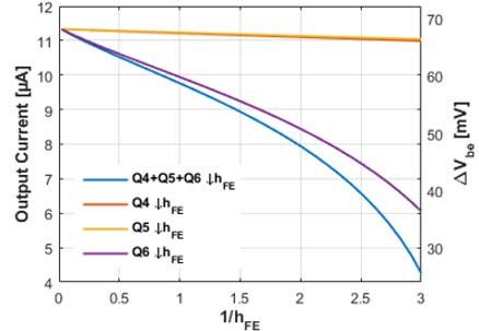
FERRARO et al.: ANALYSIS OF BIPOLAR INTEGRATED CIRCUIT DEGRADATION MECHANISMS                                                                   1591

                                                                          Fig. 10. Impact of Q2 collector to emitter current leakage (IC−E ) on LM334
Fig. 9. Impact of the degradation of the transistors Q1 and Q2 on LM334   V BE = f(V+–V− ) characteristics (top) and on the evolution of the voltage
V B E = f(V+ –V− ) characteristics (top) and on the change in V B E     required to start (VSTART) the circuit (bottom).
(bottom).

in a second time, the gain degradation of Q3–6 reaches a
saturation and the effect of the gain degradation of Q1 and
2 dominates, leading to the increase in the bandgap voltage.
The two groups of components being different kinds of tran-
sistors (PNP versus NPN), it is not surprising their degradation
does not saturate at the same levels.
   It is difficult to estimate which of Q3 or Q6 contributes
most to the decrease in the reference voltage. A scenario was
tested in simulation considering a degradation of Q3 of the
same order of magnitude as Q1 and Q2 and a degradation of
Q6 greater than the first two based on the fact that with the
same manufacturing process, PNP transistors might be more                 Fig. 11. Output current degradation observed during TID LDR irradiations
sensitive than the NPN ones. In this scenario, the degradation            with a cobalt 60 source and simulated.
of Q6 is gradually brought to saturation after having reduced
                                                                          Under these conditions, any difference in the sensitivity of
the reference voltage to 57 mV while the saturation point of the          the different transistors when exposed to different DDD/TID
Q1 and Q2 transistors is set to appear much later. The ratio of
                                                                          ratios could lead to different circuit degradation profiles.
the degradation rate of the Q3–6 group to the Q1 and Q2 group
has been selected according to the decrease rate observed
under irradiation and to their respective simulated change                D. Combined TID–DD Circuit Response
rate in the voltage reference shown previously. The resulting                The great similarity between the simulation of the evolution
degradation shape obtained by simulating this scenario scaled             of the characteristics as a function of the leakage current
to the one observed under irradiation is shown in Fig. 11.                of Q2 and the observed characteristics strongly suggests that
As it can be seen, this scenario allows achieving a good                  this mechanism is mainly responsible for circuit degradation.
approximation of the experimental curve even though only an               As mentioned above, this increase in the startup voltage has
acquisition of the degradation of the internal elements under             been observed on devices exposed to DD only and combined
irradiation could confirm it.                                             TID–DD at low ionizing dose rates while it has not been
   Considering this scenario as realistic, it is clear that total         observed on devices exposed to low ionizing dose rate only.
circuit degradation is a combination of multiple degradation              This suggests that the current leakage on Q2 is induced by
mechanisms, some mutually enhancing, others competing.                    DD effects.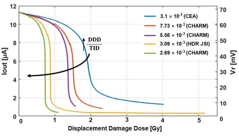
1592 IEEE TRANSACTIONS ON NUCLEAR SCIENCE, VOL. 68, NO. 8, AUGUST 2021
the impact of the current leakage on Q2 leading to the
startup voltage increase is enhanced by gain degradation of
Q6 induced by both TID and DD. This means that the effect
of the DD on the circuit is enhanced by the TID, and in a
nonlinear way.
For this reason, the experimental data are shown
in Fig. 13 as a function of the DDD. In this way, knowing
that for each curve the degradation rate for each ratio is
much higher than what could be reasonably expected from
the individual responses as shown in [3], it seems that the
experimental data support the above-presented explanation on
the increase in the degradation rate with the increase in the
ratio. Even though keeping in mind that only internal measure-
Fig. 12. Output current degradation observed during combined TID–DD ments after irradiation could give a definitive confirmation of
irradiations at the CHARM Facility and simulated. these assumptions.
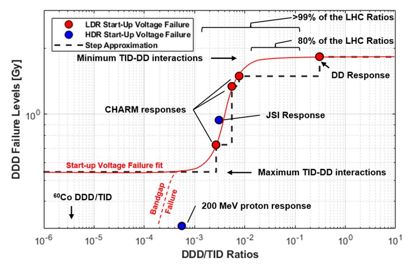
V. CERN RHA I MPLICATIONS
Considering the analysis presented in this work, it is clear
that when exposed to the LHC environment, the wide range
of DDD/TID ratios of the LHC can potentially lead to a wide
range of degradation rates for this component and potentially
many others.
Therefore, particular attention has to be paid when qualify-
ing devices potentially sensitive to such effects. Since in the
framework of regular and quantitative component RHAs such
a methodology cannot be systematically followed, due to the
relatively high amount of work to achieve such a simulation
and the fact that for commercial components the internal
Fig. 13. Simulated characteristic output current evolution observed against design is not always known, another methodology should be
TID–DD irradiation.
followed for qualification. A methodology based on DDD/TID
This scenario was tested in simulation, by applying the same ratio tests was proposed in [3], consisting of first identifying
current leakage on Q2 and Q1 transistors in addition to gain the ratio to which the system will be exposed to in operation,
degradations. Concerning these, the same parameters as for the by measurements or simulations, and second by irradiation
low ionizing dose rate simulation were kept meaning the same the devices to a certain number ratios representative of the
degradation rate for Q1–3 and Q4–Q6 with the degradation target operational environments. Then since the final step is
rate of the Q4–Q6 group higher than the Q1–Q3 group. to calculate the failure levels of the device according to the
However, in this case, a linear increase in the reciprocal current system requirements against the different ratios and to verify
gain corresponding to the DD effects is applied in addition to that it is compliant with the radiation levels associated with
the TID-induced degradations. This will have as effect that the different ratios in operation.
there will be no saturation of the damages, and therefore For instance, for the studied device, the different failure
the initial degradation mechanisms including the decrease in levels calculated for a maximum variation in 30% of the
the output current will never be compensated by the second initial output current for the different tested ratios are shown
degradation mechanism inducing its increase. in Fig. 14. In this figure, the failure levels obtained with
The resulting simulated output degradation is visible combined TID–DD response with HDR TID are marked in
in Fig. 12, while the evolution of the current characteristics blue since they are not representative of the real behavior.
is visible in Fig. 13 in comparison to the experimental data. The two failure fits are figures of merit calculated from the
As it is visible, the simulated response achieves a good simulation models together with the additional assumptions
approximation of the experimental data once normalized to that below ratios of 10−3 , the DD becomes negligible and
the same dose. Especially the shape of the evolution of the above ratios of 0.1 the TID becomes negligible, and thus
characteristic is particularly close to the experimental one. the failure levels are constant since there is no interaction
Therefore, the assumptions used for simulation seem to be between the different effects. For the fits, the second failure
reasonably representative of the real degradation mechanisms, contribution called “bandgap failure” concerns the case where
even though only the monitoring of the internal transistor the degradation limit is overpassed due to the drift of the
degradations could confirm it. bandgap voltage due to the TID contribution only.
Finally, the most important outcome of this simulation is It can be seen from the figure that in the case of this
the fact that the combined TID–DD circuit response is due to: component, for about 80% of the ratios the device will be
1) gain degradations induced by TID and DD and 2) current exposed to in operation, the device will show a very low
leakage induced by DD only. Then, as shown in Fig. 10, level of combined TID–DD circuit effects, while for the 20%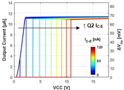
FERRARO et al.: ANALYSIS OF BIPOLAR INTEGRATED CIRCUIT DEGRADATION MECHANISMS                                                                                      1593

                                                                                       observed against TID only and combined TID–DD. Besides
                                                                                       being in good agreement with the experimental data, these
                                                                                       circuits simulations have shown that the impact of the DD
                                                                                       that seems to be induced in one of the transistors on the
                                                                                       circuit response can be enhanced by the degradation of the
                                                                                       current gain of another transistor in the circuits induced by
                                                                                       TID and DD. Therefore, it has been shown that the level of
                                                                                       interaction between these two mechanisms seems to depend on
                                                                                       the DDD/TID ratio, which is in agreement with the observed
                                                                                       increased degradation rate as a function of the ratios.

                                                                                                                      R EFERENCES
                                                                                        [1] H. J. Barnaby et al., “Identification of degradation mechanisms in a
                                                                                            bipolar linear voltage comparator through correlation of transistor and
Fig. 14. LM334 failure levels expressed in DDD for different DDD/TID                        circuit response,” IEEE Trans. Nucl. Sci., vol. 46, no. 6, pp. 1666–1673,
ratios obtained in different test facilities. Failures levels correspond to a change        Dec. 1999, doi: 10.1109/23.819136.
in the current output above a ±30% tolerance. The two failure fits are figured          [2] H. Barnaby, H. J. Tausch, R. Turfler, P. Cole, P. Baker, and R. L. Pease,
of merit calculated from the simulation model.                                              “Analysis of bipolar linear circuit response mechanisms for high and
                                                                                            low dose rate total dose irradiations,” IEEE Trans. Nucl. Sci., vol. 43,
                                                                                            no. 6, pp. 3040–3048, Dec. 1996, doi: 10.1109/23.556903.
remaining the combined effects are a real driving factor to be                          [3] R. Ferraro et al., “Study of the impact of the LHC radiation envi-
considered for qualification. Such a qualification methodology                              ronments on the synergistic displacement damage and ionizing dose
can then be applied without the need of performing simulations                              effect on electronic components,” IEEE Trans. Nucl. Sci., vol. 66, no. 7,
                                                                                            pp. 1548–1556, Jul. 2019, doi: 10.1109/TNS.2019.2902441.
or knowledge of the internal structure.
                                                                                        [4] R. K. Freitag and D. B. Brown, “Study of low-dose-rate radiation effects
                                                                                            on commercial linear bipolar ICs,” IEEE Trans. Nucl. Sci., vol. 45, no. 6,
                                                                                            pp. 2649–2658, Dec. 1998, doi: 10.1109/23.736510.
                             VI. C ONCLUSION                                            [5] A. H. Johnston, G. M. Swift, and B. G. Rax, “Total dose effects in
                                                                                            conventional bipolar transistors and linear integrated circuits,” IEEE
   In this work, it has been introduced that integrated circuits                            Trans. Nucl. Sci., vol. 41, no. 6, pp. 2427–2436, Dec. 1994, doi:
sensitive to both TID and DD effects could exhibit combined                                 10.1109/23.340598.
TID–DD circuit effects when exposed to both effects simul-                              [6] L. Dusseau et al., “Review and analysis of the radiation-induced degra-
taneously. Such interactions between the internal degradation                               dation observed for the input bias current of linear integrated circuits,”
                                                                                            IEEE Trans. Nucl. Sci., vol. 55, no. 6, pp. 3174–3181, Dec. 2008, doi:
mechanisms could lead a component to exhibit a various range                                10.1109/TNS.2008.2006835.
of degradation profiles when exposed to a wide range of                                 [7] R. N. Nowlin, D. M. Fleetwood, R. D. Schrimpf, R. L. Pease,
DDD/TID ratios such as the ones that can be found in high-                                  and W. E. Combs, “Hardness-assurance and testing issues for bipo-
                                                                                            lar/BiCMOS devices,” IEEE Trans. Nucl. Sci., vol. 40, no. 6,
energy accelerator environments.                                                            pp. 1686–1693, Dec. 1993, doi: 10.1109/23.273492.
   To give an example of how TID- and DD-induced degrada-                               [8] R. L. Pease et al., “Evaluation of proposed hardness assurance method
tion mechanisms can interact at the circuit level depending                                 for bipolar linear circuits with enhanced low dose rate sensitivity
                                                                                            (ELDRS),” IEEE Trans. Nucl. Sci., vol. 45, no. 6, pp. 2665–2672,
on the DDD/TID ratio, degradation simulations have been                                     Dec. 1998, doi: 10.1109/23.736512.
performed on the internal circuit of a case study component,                            [9] LM234 Datasheet. Accessed: Mar. 21, 2021. [Online]. Available:
the LM334, which has been shown to be sensitive to this effect                              https://www.st.com/resource/en/datasheet/lm234.pdf
in previous work.                                                                      [10] F. Pozzi et al., “CERN irradiation facilities,” Radiat. Protection Dosime-
                                                                                            try, vol. 180, nos. 1–4, pp. 120–124, Aug. 2018.
   Thanks to the additional TID irradiations that have been                            [11] A. Akkerman, J. Barak, M. B. Chadwick, J. Levinson, M. Murat,
performed at different dose rates, three different degradation                              and Y. Lifshitz, “Updated NIEL calculations for estimating the damage
mechanisms have been identified; one inducing the decrease                                  induced by particles and γ -rays in Si and GaAs,” Radiat. Phys. Chem.,
                                                                                            vol. 62, no. 4, pp. 301–310, Oct. 2001.
in the output current, one inducing the increase in the output                         [12] A. Shatalov, S. Subramanian, and A. Klein, “Correlation between
current, and the last one inducing the increase in the startup                              nonionizing energy loss and the offset voltage shift in InP-InGaAs
voltage. Then, to understand the cause of these different                                   heterojunction bipolar transistors,” IEEE Trans. Nucl. Sci., vol. 48, no. 6,
                                                                                            pp. 2262–2269, Dec. 2001.
mechanisms, a SPICE model reproducing the characteristic
                                                                                       [13] J. Morin et al., “The PROSPERO and CALIBAN neutron irradia-
of the component based on the internal circuit given in the                                 tion facilities,” in Proc. 1st Eur. Conf. Radiat. Effects Devices Syst.
datasheet has been built.                                                                   (RADECS), La Grande-Motte, France, Sep. 1991, pp. 574–576. [Online].
   Afterward, a first set of simulations have been performed                                Available: https://doi.org/10.1109/RADECS.1991.213535
                                                                                       [14] H. J. Barnaby, R. D. Schrimpf, A. L. Sternberg, V. Berthe, C. R. Cirba,
where the impacts of a current gain decrease and the emitter                                and R. L. Pease, “Proton radiation response mechanisms in bipolar
current leakage of each transistor on the circuit’s response                                analog circuits,” IEEE Trans. Nucl. Sci., vol. 48, no. 6, pp. 2074–2080,
were analyzed. From this analysis, it has been shown that                                   Dec. 2001, doi: 10.1109/23.983175.
                                                                                       [15] V. Ramachandran et al., “Modeling total-dose effects for a low-dropout
the three different observed degradation mechanisms could                                   voltage regulator,” IEEE Trans. Nucl. Sci., vol. 53, no. 6, pp. 3223–3231,
be reported to the degradation of three different groups of                                 Dec. 2006, doi: 10.1109/TNS.2006.885377.
transistors.                                                                           [16] J. Mekki, M. Brugger, R. G. Alia, A. Thornton, N. C. D. S. Mota,
   Finally, from this analysis, two circuit degradation scenarios                           and S. Danzeca, “CHARM: A mixed field facility at CERN for radia-
                                                                                            tion tests in ground, atmospheric, space and accelerator representative
were proposed, combining specific degradation conditions                                    environments,” IEEE Trans. Nucl. Sci., vol. 63, no. 4, pp. 2106–2114,
for those three groups, to reproduce the degradation profiles                               Aug. 2016, doi: 10.1109/TNS.2016.2528289.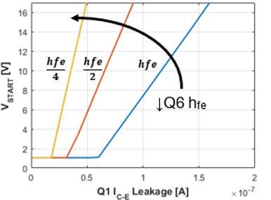
You can also read