Call For Participation ISPD Benchmark Contest 2021 Wafer-Scale Physics Modeling
←
→
Page content transcription
If your browser does not render page correctly, please read the page content below
Call For Participation
                               ISPD Benchmark Contest 2021
                               Wafer-Scale Physics Modeling
                     A new frontier for partitioning, placement and routing

                     Michael James, Patrick Groeneveld, Vladimir Kibardin, Ilya Sharapov, Marvin Tom
                                          Cerebras Systems, Los Altos, CA, USA

Summary
The ACM International Symposium on Physical Design (ISPD) in collaboration with Cerebras
Systems will organize the 2021 ISPD benchmark contest. The contest will run from December
through mid March 2021. The registration is open! The latest details with registration
information will be posted at www.ispd.cc and www.cerebras.net/ispd-2021-contest/ .
The 2021 edition of the ISPD benchmark competition features an innovative twist on traditional
Physical Design. The task is to map a 3-D Finite Element model on a 2-D grid of processing
elements in a supercomputer. The objectives are to maximize performance and accuracy, while
minimizing interconnect length. This involves partitioning and placement algorithms.
Participating teams will be supplied benchmark examples and an open source program to
evaluate the score of their program. The results will be judged on a set of ‘blind’ benchmarks. As
in 2020, substantial prizes will be given to the best teams.

Introduction
Finite Element (FE) methods are widely used for solving nonlinear partial differential equations
(PDE’s). They use a mesh of discrete points to model a region. FE methods perform the same
computational pattern uniformly at all mesh points. Fast computation of Finite Element
methods has many relevant applications in engineering: from aerodynamics and structural
analysis, calculating heat transfer to electromagnetic potentials. Typically, FE methods are run
on clusters of CPUs and accelerated using GPUs.
For the 2021 ISPD contest we will run FE on a massive homogenous multiprocessor: the
Cerebras CS-1. This is an opportunity to show that our Physical Design algorithms are applicable
outside of the traditional IC domain. Running FE on the CS-1 requires a good application of
typical Physical Design algorithms: partitioning followed by placement (or a combination of the
two). For the placement either block or standard cell placer techniques are applicable.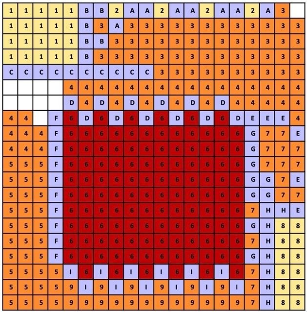
The Cerebras CS-1 wafer scale supercomputer consists of over 400,000 identical processing
elements on a single wafer. Each such element is a fully programmable compute core with 48kB
of memory that is capable of running a dedicated program. At 21.5cm by 21.5 cm and with 1.2
trillion transistors, the CS-1 is the largest monolithic computer chip in the world. The total
memory adds up to 18GB of fast on-chip memory. Until now the CS-1 was mainly used to
accelerate training for machine learning. That was also what the 2020 ISPD contest was about.
In 2021 we will extend the application of the CS-1 to physics emulation with FE methods.
The 2-D mesh arrangement of the processing elements makes the CS-1 quite suitable for mesh-
style FE methods (aka stencil problems). We recently demonstrated that CS-1 is capable of
emulating over a million mesh points in real time: a first. Thanks to the suitability for stencil
problems the CS-1 achieves a performance that is 10,000 times (!!) faster than a GPU node. It
will even be 200 times faster than any supercomputer cluster, no matter how large that cluster
is. This is because the algorithms used to evaluate stencil codes are fundamentally limited in
their strong scaling on clusters by communication latency.
As a result, new applications will be unlocked. For example, faster than real time emulation
could improve weather prediction or could provide immediate actionable data for oil spill
containment. And in industrial design, the shape of a manifold may be optimized via gradient
descent using data from many consecutive emulations.
To speed up the Finite Element mesh emulation most practical physics problems do not use a
uniform grid. Instead, the space is partitioned in localized regions of high interest around
discontinuities, while a coarser mesh is used in less dynamic areas. For example, when studying
an aircraft wing the important quantities such as lift are functions of the air flow at the wing
and body surfaces. There can be a complex flow in this boundary layer. Thus, the flow near the
leading edge and tip of the wing are more important and require more accuracy and resolution
than the flow in the largely empty space between the surface of the wing and the aircraft’s hull.
As described, the mesh size of the finite elements used for modelling varies in different parts of
the space. This enables a significant speedup, at the price of some additional algorithmic steps
to glue regions with different mesh resolutions together.
And that is exactly what the 2021 ISPD benchmark contest is about. As will become clear, EDA
physical design algorithms are key in this process.

Benchmark Description
The task is to efficiently map a realistic 3-dimensional Finite Element problem onto the 2-
dimensional array of 633 by 633 processing elements of the CS-1 supercomputer.
The problem is presented as a 3D volume (space) that a user desires to model. Also given is a
real-valued heatmap v:x,y,zà[0,1] that describes the desired relative grid resolution of every
point in the modelled space.
The first problem is to partition the space into rectangular prisms. Each prism is assigned a
resolution which determines the number of grid-points that it contains. The prism’s
computation will be implemented as a kernel which is an arrangement of processing elements.
A kernel must communicate with all other neighboring kernels that it shares a boundary with.
The programmable routing of the CS-1 Network-on-Chip fabric are used for this
communication. The routing fabric much resembles a maze routing problem with 24 layers.
An adapter kernel is required in case the resolution of adjacent prisms is different. This kernel is
also built using processing elements. It interpolates the resolution differences across the
boundary. The relative resolution adaptation is always a factor of 2 (for simplicity).
The regular stencil kernel that is used as a building block requires memory proportional to the
number of mesh points that it models. It requires fabric bandwidth to talk to its neighbors that
is proportional to the surface area of its boundary.
Before addressing placement, we first need to describe the Processing Element (PE) and the
routing fabric in a little more detail. Each PE contains a processor CPU with 48Kb SRAM memory
that is connected via a network interface to the Network-on-Chip fabric. A PE can receive and
send a data packet to any of its 4 neighboring PEs simultaneously. Every clock cycle that packet
can hop to a neighboring PE in any direction. 24 different packets can be multiplexed over the
same connection. By programming the packet forwarding table a routing pattern can be
encoded that facilitates high-bandwidth communication between PEs. This forwarding pattern
also makes up the routes of the ‘wires’ along which the messages travel. In practice this is
similar to a maze routing problem with 24 layers. But in contrast to IC or FPGA routing the wires
carry 32-bit packets, rather than 1-bit signals.
To simplify the contest, we will not consider the detailed routing, local congestion nor
bandwidth contention uses due to packets sharing the same physical connection. Instead we
capture overall quality by measuring total half-perimeter wire length between all PEs. The
shorter the wires on average, the better.
In contrast to conventional IC/FPGA routing the delays of long wires are much less of a
problem. In the steady state the data streams at a constant rate irrespective of the path length.
The main reason to minimize wire length is to avoid congestion issues during routing and
interference when multiplexing different packet types. In practice the routing resources are
limited to 24 different signals across each connection. To simplify the benchmark, we will only
consider the total wire length instead of the actual routing and congestion.
The processing element (PE) is programmed to do one of 3 tasks in this context:
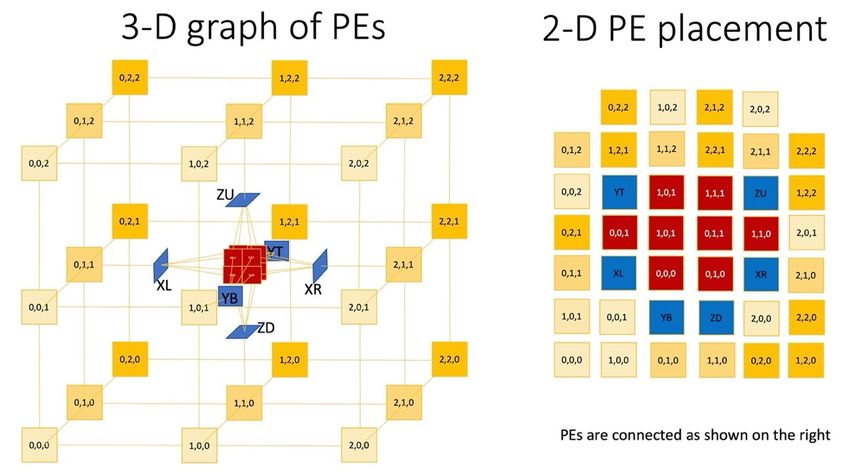
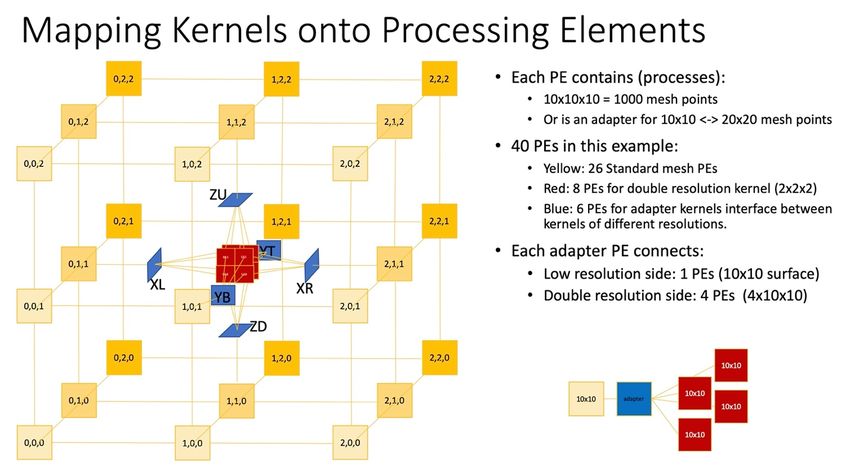
1. Mesh PE: Solves differential equations in 10x10x10 = 1000 mesh points of the kernel.
Therefore, the amount of computation and memory in a PEs is the same irrespective of
the resolution. The mesh PE communicates with at most 6 neighboring PEs only (XL, XR,
YB, YT, ZD, ZU). This means that the PEs in a kernel form a 3-D regular mesh. In the
example above the standard resolution kernels are each 10x10x10, so fit in 1 PE.
A kernel with twice the mesh resolution will therefore require 8 times the number of
PEs, and with that 8 times as many PEs.
2. Adapter PE: Resolves mesh resolution differences through interpolation at the
boundary between kernels of different resolution by interpolation. It has two
(bidirectional) connections: one to the PE with the higher resolution and one to the PE
with the lower resolution. On the lower-resolution side the adapter connects to 1 PE ro
10X10 boundary mesh points. On the higher resolution side, it connects to 20x20 mesh
points. This means it connects to 4 PEs as show in the figure above
3. Unused PE: A PE that runs no program, yet the network interface can forward packets in
all directions. There should be as few as possible unused PEs.
Since the emulation rate is a function of the number of emulated mesh points, we aim to
maximize the number of mesh PEs. The more adapter PEs, the slower the emulation because
the remaining mesh PE each need to process more mesh points.
Now we are ready for placement of the kernels on the 2-D array of 633 by 633 PEs. There could
be two ways address this task:
   1. Place the kernels as rectangular blocks using a block level placer. This preserves the
      optimal internal 2-D structures of the kernels.
   2. Perform a flat PE-level placement using a cell level placer. This breaks up the internal
      mesh structures, preserving the net list
Each approach will have it advantages and disadvantages. Which one is picked is up to the
team. The objective of the placement is to fit the mesh- and adapter PEs in a non-overlapping
way such that total wire length is minimized.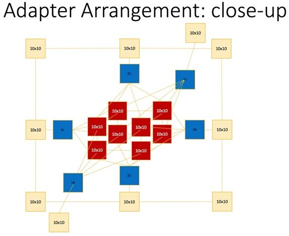
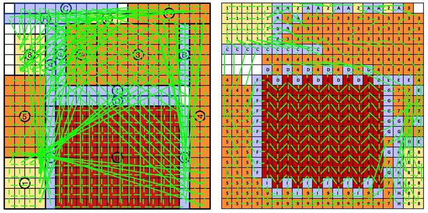
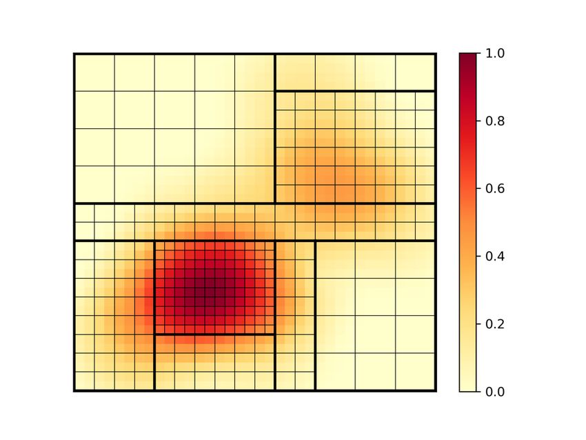
The overall objective for the problem is to find a valid mapping that maximizes fidelity in the
regions of interest while also maximizing the emulation rate. Details on how the trade-off is
measured are below.

Benchmark Illustration
The figures below illustrate the entire process on a toy example using a 2-D space rather than a
3D space. First assume we are given the following 2D heat map with a resolution function from
yellow to dark red. The dark red area has target resolution of 0.8, which is 4X more than the
target resolution in the yellow areas. Also shown is a possible partitioning into 8 regions with 3
different resolutions. Different partitions are possible.

Assume that – rather than the actual 623 by 623 PEs - we have a grid of 20 by 20 PEs = 400 PEs
total. Estimating the kernel overhead to be 25%, so ¾ of the 400 PEs is available for the mesh
kernels. That leaves 100 PEs for adapter kernels and some empty kernels. The exact number
will need to be calibrated. So now we can draw the above using 304 mesh PEs:

The 8 mesh kernels are numbered 1 through 8. Each of these regions is a rectangular kernel of
w by h PEs. The lines indicate the required wires between the kernels. The area (the number of
processing elements) is proportional to the number of mesh points the region contains. The
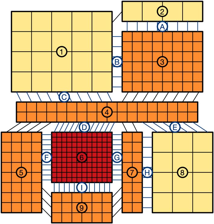
lowest resolution is drawn in yellow, the medium resolution in orange and the highest
resolution in red. Wires connect the processing elements and the different regions. In case the
resolution of the regions is different, an interpolation adapter is needed. These adapters are
marked A thru I. For instance: the adapter E between kernels 4 and 8 adjusts the resolution
from 1 to 2 and vice versa. Kernels 3 and 4 do not need an adapter because their resolution is
the same.
Each square in the above picture is a PE. This means that the actual size of module 3 is much
bigger than module 1. Below shows a possible block level (left) and PE-level (right) placements
on a 20x20 die. These example placements are hand-generated in PowerPoint:

The adapter kernels are blue and marked by their letter (note: these adapters are larger,
following a different sizing than the actual benchmark). The mesh kernels are colored according
to their resolution and marked by their number. Unused PEs are marked white. In the block
placement the kernels are preserved as-is, so the adapter kernels are in the spaces around the
kernels. In the flat PE-level placement the PEs can mix, and the kernels may be deformed to fit
the shape.

The picture below shows hand-routed results for both option with the nets shown as fly-lines.
The actual routed wires would be orthogonal, but for the purpose of the benchmark we will just
count half-perimeter wire length.
Benchmark Formulation
Input
   1. 3D bounding region
   2. Target resolution function v: x,y,z ® [0,1] . The larger the value of v, the finer
      discretization is desired. For example, a point with resolution v=0.8 has twice the
      desired resolution as a point with v=0.4.
   3. A 633x633 compute fabric of ~400,000 Compute Elements. Each PE can process
      10x10x10 = 1000 grid points, or be an adapter between 10x10 and 20x20 grid points.
Volume Partitioning
   1. The bounding region should be covered by a finite set of 3D prisms (regions).
   2. Prisms contain non-overlapping mesh points.
   3. The solution should specify the discretization resolution of each prism (same in all three
      spatial dimensions x, y and z)
   4. The resolution ratio between two adjacent regions can only be 1:1 or 1:2.
   5. Adapter kernels should be provisioned for every pair of prisms with different resolution
      whose boundaries touch.
Placement Legality Constraints
   1.   Kernels are mapped to rectangular x by y regions on the waver-scale engine.
   2.   An adapter is a 1 by n array of PEs, where n is the largest number of PEs on the edge.
   3.   All kernels fit within the WSE area of 633x633 Processing Elements.
   4.   No PEs overlap
5. Adapters may be placed non-overlapping. They may be ‘fused’ (or glued) to a kernel.
The more adapters are used, the less PEs are available for computation.
6. Upper-bound of solver run-time (e.g., place and route complete in < 8 hours).
Optimality Objective
1. The overall goal is to minimize the time for each iteration of a solver, such as the
BiConjugate Gradient algorithm, while maximizing the accuracy of the approximation.
2. The accuracy of the approximation is optimized when the normalized density of the
partitioning (v') is the closest to the heatmap v. We measure it as the integral L
2-norm of the difference of the target and placement densities. Since matching the
density of high-resolution regions is more important we use v as the weight function in
the L2-norm
3. The communication overhead of the placement is determined by the total half-perimiter
wire length of connections between regions. We use the L1.5-norm for this metric.
Unlike the L1-norm it disproportionally penalizes long connections but not as severely as
the L2 norm.
The overall score will be a linear combination of both metrics Fr and Fw with given weights:You can also read