Charge generation of large-area dynode photomultiplier tubes
←
→
Page content transcription
If your browser does not render page correctly, please read the page content below
Charge generation of large-area
 dynode photomultiplier tubes

                   von
                Troy Swift

         Masterarbeit in Physik

                vorgelegt der
 Fakultät für Mathematik, Informatik und
 Naturwissenschaften der RWTH Aachen

              17.Oktober 2018

               angefertigt am
      III. Physikalischen Institut B

                    bei
          Prof. Dr. Achim Stahl
     Prof. Dr. Christopher Wiebusch
1. Gutachter : Prof. Dr. Achim Stahl

2. Gutachter : Prof. Dr. Christopher Wiebusch

Datum des Einreichens der Arbeit: 17.10.2018
Contents

1 Introduction                                                                                                                  9

2 Neutrino oscillations                                                         11
  2.1 Survival probability and mass hierarchy . . . . . . . . . . . . . . . . . 11

3 JUNO project                                                                     13
  3.1 Collaboration . . . . . . . . . . . . . . . . . . . . . . . . . . . . . . . 13
  3.2 Physics program . . . . . . . . . . . . . . . . . . . . . . . . . . . . . 13
  3.3 Detector . . . . . . . . . . . . . . . . . . . . . . . . . . . . . . . . . . 13

4 Hamamatsu large-area dynode PMT                                            19
  4.1 Dynode PMT design & function . . . . . . . . . . . . . . . . . . . . . 19

5 Data measurement and processing                                                                                              23
  5.1 Motivation to generate charge spectra . . . . . . . . . . . . . . .                                          .   .   .   23
  5.2 Experimental setup and DAQ . . . . . . . . . . . . . . . . . . .                                             .   .   .   23
      5.2.1 PMT . . . . . . . . . . . . . . . . . . . . . . . . . . . . .                                          .   .   .   23
      5.2.2 Lightproofing . . . . . . . . . . . . . . . . . . . . . . . .                                          .   .   .   24
      5.2.3 Signal generator & light-emitting diode (LED) . . . . . .                                              .   .   .   24
      5.2.4 HV supply & gate/delay module . . . . . . . . . . . . . .                                              .   .   .   24
      5.2.5 Evaluation board with analog-to-digital converter (ADC)                                                .   .   .   25
  5.3 Data processing . . . . . . . . . . . . . . . . . . . . . . . . . . .                                        .   .   .   25
      5.3.1 Charge integration . . . . . . . . . . . . . . . . . . . . .                                           .   .   .   25

6 Modeling PMT charge response                                                                                                 27
  6.1 Motivation . . . . . . . . . . . .   .   .   .   .   .   .   .   .   .   .   .   .   .   .   .   .   .   .   .   .   .   27
  6.2 Charge amplification at dynodes      .   .   .   .   .   .   .   .   .   .   .   .   .   .   .   .   .   .   .   .   .   27
      6.2.1 Charge acceleration . . .      .   .   .   .   .   .   .   .   .   .   .   .   .   .   .   .   .   .   .   .   .   27
      6.2.2 Dynode coatings . . . .        .   .   .   .   .   .   .   .   .   .   .   .   .   .   .   .   .   .   .   .   .   27
  6.3 Model fit-parameters . . . . . .     .   .   .   .   .   .   .   .   .   .   .   .   .   .   .   .   .   .   .   .   .   28
      6.3.1 nWidth . . . . . . . . .       .   .   .   .   .   .   .   .   .   .   .   .   .   .   .   .   .   .   .   .   .   28
      6.3.2 Gain . . . . . . . . . . .     .   .   .   .   .   .   .   .   .   .   .   .   .   .   .   .   .   .   .   .   .   28
      6.3.3 RPE . . . . . . . . . . .      .   .   .   .   .   .   .   .   .   .   .   .   .   .   .   .   .   .   .   .   .   29
      6.3.4 DynExp . . . . . . . . .       .   .   .   .   .   .   .   .   .   .   .   .   .   .   .   .   .   .   .   .   .   29
      6.3.5 PSkip . . . . . . . . . .      .   .   .   .   .   .   .   .   .   .   .   .   .   .   .   .   .   .   .   .   .   29
  6.4 Peaks within valleys . . . . . .     .   .   .   .   .   .   .   .   .   .   .   .   .   .   .   .   .   .   .   .   .   29
      6.4.1 Peak-to-valley ratio . . .     .   .   .   .   .   .   .   .   .   .   .   .   .   .   .   .   .   .   .   .   .   30

                                         3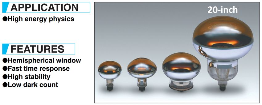
6.4.2 Direct triggering and PMT      efficiency        .   .   .   .   .   .   .   .   .   .   .   .   .   .   31
   6.5   Simulation walkthrough . . . . .     . . . . . .       .   .   .   .   .   .   .   .   .   .   .   .   .   .   31
         6.5.1 Simulation stage I . . . . .   . . . . . .       .   .   .   .   .   .   .   .   .   .   .   .   .   .   31
         6.5.2 Simulation stage II . . . .    . . . . . .       .   .   .   .   .   .   .   .   .   .   .   .   .   .   32
         6.5.3 Simulation stage III . . . .   . . . . . .       .   .   .   .   .   .   .   .   .   .   .   .   .   .   33
         6.5.4 Comprehensive flow chart       . . . . . .       .   .   .   .   .   .   .   .   .   .   .   .   .   .   33

7 Parameter minimization                                                                                                35
  7.1 Concepts & techniques . . . . . . . . .       .   .   .   .   .   .   .   .   .   .   .   .   .   .   .   .   .   35
      7.1.1 Stochastic fluctuations . . . . .       .   .   .   .   .   .   .   .   .   .   .   .   .   .   .   .   .   35
      7.1.2 Goodness-of-fit . . . . . . . . .       .   .   .   .   .   .   .   .   .   .   .   .   .   .   .   .   .   35
      7.1.3 Oversampling . . . . . . . . . .        .   .   .   .   .   .   .   .   .   .   .   .   .   .   .   .   .   36
  7.2 Migrad minimizer . . . . . . . . . . . .      .   .   .   .   .   .   .   .   .   .   .   .   .   .   .   .   .   36
      7.2.1 Coaxing convergence . . . . . .         .   .   .   .   .   .   .   .   .   .   .   .   .   .   .   .   .   36
      7.2.2 Pull . . . . . . . . . . . . . . .      .   .   .   .   .   .   .   .   .   .   .   .   .   .   .   .   .   39
  7.3 Simplex pseudo-minimizer . . . . . . .        .   .   .   .   .   .   .   .   .   .   .   .   .   .   .   .   .   40
      7.3.1 Comparison of two models . . .          .   .   .   .   .   .   .   .   .   .   .   .   .   .   .   .   .   42
      7.3.2 Fake-data testing with Simplex          .   .   .   .   .   .   .   .   .   .   .   .   .   .   .   .   .   44

8 Summary and outlook                                                                                                   47

9 Appendix                                                                                                              49
  9.1 A: gain approximation . . . . . . . . . .         .   .   .   .   .   .   .   .   .   .   .   .   .   .   .   .   49
  9.2 B: PSkip’s influence on charge spectrum           .   .   .   .   .   .   .   .   .   .   .   .   .   .   .   .   51
  9.3 C: noise reduction via oversampling . . .         .   .   .   .   .   .   .   .   .   .   .   .   .   .   .   .   52
  9.4 D: Hamamatsu 20” PMT base diagram .               .   .   .   .   .   .   .   .   .   .   .   .   .   .   .   .   53

10 Acknowledgements                                                                                                     57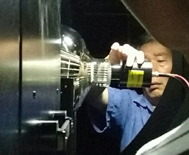
List of Figures
2.1 Expected composition of reactor neutrino flux at 4 MeV [17]. . . . . . 11
2.2 Neutrino mass hierarchy patterns: normal vs. inverted. Mass eigen-
states are indexed numerically, while flavor eigenstates are indexed
e, µ, τ (image adapted from [3]). . . . . . . . . . . . . . . . . . . . . . 12
3.1 Pre-JUNO simulated e+ spectrum of IBDs from a reactor ν̄ idealized
experiment using a 20 kton detector with a 40 GWth reactor 58 km
away [18]. . . . . . . . . . . . . . . . . . . . . . . . . . . . . . . . . . 14
3.2 JUNO regional map [1, 2, 3, 4]. Both Taishan and Yangjiang nuclear
power plant sit ∼ 53 km from the JUNO detector. . . . . . . . . . . 15
3.3 Civil construction schematic for subterranean portion of JUNO [from
internal communication] . . . . . . . . . . . . . . . . . . . . . . . . . 16
3.4 IBD diagram and measured spectrum [17]. . . . . . . . . . . . . . . 16
3.5 Diagram of JUNO detector [15] . . . . . . . . . . . . . . . . . . . . . 17
4.1 PMTs [5] . . . . . . . . . . . . . . . . . . . . . . . . . . . . . . . . . . 20
4.2 20” PMT socketing into base at container-testing facility near JUNO 20
4.3 Simplified layout of a dynode-based PMT [5] . . . . . . . . . . . . . . 21
5.1 Experimental setup [6] . . . . . . . . . . . . . . . . . . . . . . . . . . 24
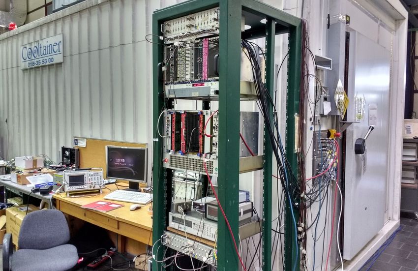
5.2 Container plus all exterior electronics . . . . . . . . . . . . . . . . . . 25
5.3 Miss-rates for various NPE , with typical simulation parameters [6] . . 26
5.4 PMT signal [6] . . . . . . . . . . . . . . . . . . . . . . . . . . . . . . 26
6.1 Secondary emission ratio for assorted dynode coatings [7] . . . . . . . 28
6.2 Charge spectrum: contributions to the valley (circled) are of primary
interest. . . . . . . . . . . . . . . . . . . . . . . . . . . . . . . . . . . 30
6.3 Previous, cruder method for fitting a PMT charge spectrum [8] . . . . 30
6.4 Simulation stage I [6] . . . . . . . . . . . . . . . . . . . . . . . . . . . 31
6.5 Simulation stage II [6] . . . . . . . . . . . . . . . . . . . . . . . . . . 32
6.6 Simulation stage III [6] . . . . . . . . . . . . . . . . . . . . . . . . . . 33
6.7 Simulation overview including dynode skip probabilities [6] . . . . . . 33
7.1 Smoothing effect of higher simulation oversampling factors . . . . . . 37
7.2 The benefits of more measured data . . . . . . . . . . . . . . . . . . . 38
7.3 Extreme examples of stochastic noise obscuring the minimum of a
scan-parabola . . . . . . . . . . . . . . . . . . . . . . . . . . . . . . . 39
5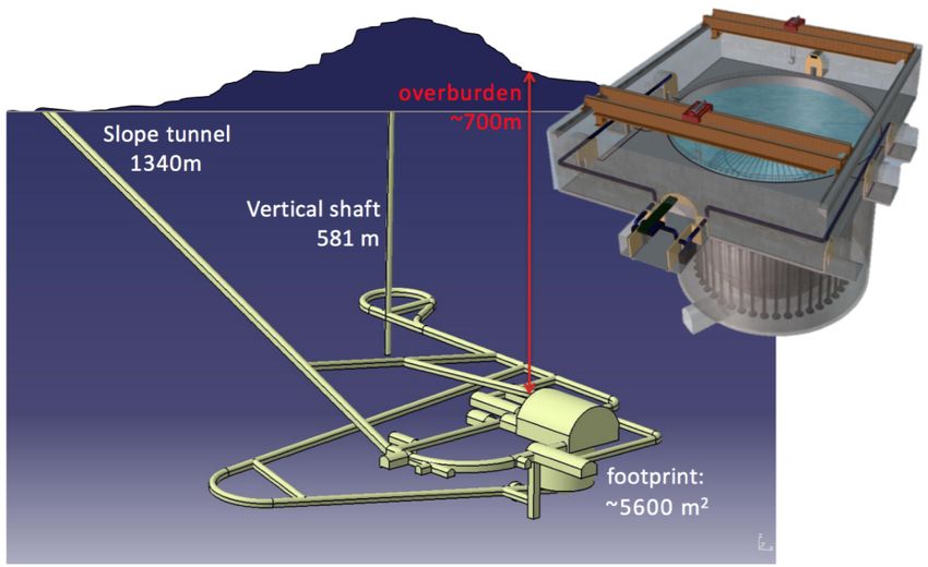
7.4   Pull distributions: an investigation into the extreme scan-values from
      Figure 7.3 . . . . . . . . . . . . . . . . . . . . . . . . . . . . . . . .   . 40
7.5   Typical results for parameter fits to both models . . . . . . . . . . .      . 41
7.6   Model 2 charge spectra: data vs. simulation seeded with best-fit
      parameters . . . . . . . . . . . . . . . . . . . . . . . . . . . . . . . .   . 42
7.7   Model 2 charge spectra: data vs. simulation seeded with best-fit
      parameters . . . . . . . . . . . . . . . . . . . . . . . . . . . . . . . .   . 43
7.8   Typical fake-data results for parameter-fits to both models . . . . .        . 45

9.1   Measured PMT gain as function of HV, plotted log-log; reference to
      ideal JUNO gain at [9] (p.138) . . . . . . . . . . . . . . . . . . . . . . 50
9.2   Simulation response to varying first-dynode skip probability . . . . . 51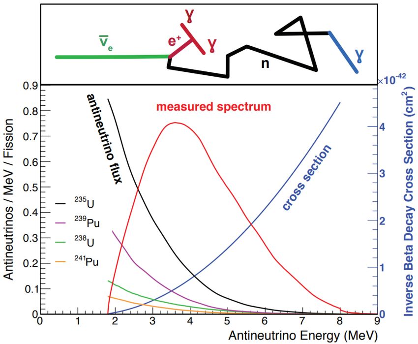
List of Tables

 2.1   3-neutrino oscillation parameters, global fit. Values are for normal
       (inverted) mass hierarchy (see Figure 2.2) [16]. . . . . . . . . . . . . . 12

 7.1   Fake-data parameter fits for Model 1 . . . . . . . . . . . . . . . . . . 46
 7.2   Fake-data parameter fits for Model 2 . . . . . . . . . . . . . . . . . . 46

                                        7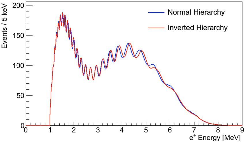
Chapter 1

Introduction

Reactor neutrino experiments have been an important part of neutrino research for
six decades, ever since Reines and Cowan discovered neutrinos in 1956 [21]. The
most recent generation of fully operational experiments were Daya Bay [22], Double
Chooz [23], and RENO [24], which were designed in the 2000s and perhaps most
notably measured the smallest mixing angle θ13 by observing reactor antineutrino
(ν̄e ) oscillations at a baseline of ∼ 1 km.
      The JUNO (Jiangmen Underground Neutrino Observatory) collaboration is cur-
rently constructing a next-generation liquid scintillator neutrino detector in China.
Data-taking is expected to be underway by 2021. The main goal of JUNO’s physics
program is to better understand the neutrino mass hierarchy and to measure the
neutrino mixing parameters sin2 θ12 , ∆m221 , and ∆m2ee to within 1 % uncertainty
[15].
      JUNO will be supplied with reactor antineutrinos from the Yangjiang and Tais-
han nuclear power plants. The JUNO detector is positioned 53 km from both power
plants. The central detector houses an acrylic sphere 35 m in diameter filled with
20ktons of LAB-based liquid  p scintillator. JUNO’s mission requires an unprecedented
energy resolution of 3 %/ E (MeV) at 1 MeV. Crucial to this resolution is the per-
formance of an inward-looking array of 18,000 20-inch large area PMTs plus 25,000
3-inch PMTs [3].
      The primary goal of this research is to better characterize charge amplification
processes within JUNO’s 5,000 large-area Hamamatsu dynode PMTs, in order de-
liver the best detector energy resolution. Optimization of the PMT base supports
this effort.
      Development of PMT charge-response models requires frequent validation against
real measured data. Charge spectra histogrammed from the integrated charge of
single events are the preferred format for direct comparison between simulated and
measured data.
      The models developed during this research generate a PMT charge response from
first principles, from which a charge spectrum is then histogrammed and evaluated.
The section greatest interest within the charge spectrum is the “valley” of interme-
diate Ne− values between the noise peak and 1 PE peak, since this range is home
to most charge signals resulting from ≥ 1 dynode skips during PMT amplification.
Since JUNO’s operational mode involves direct triggering on PMT signals, the low

                                          9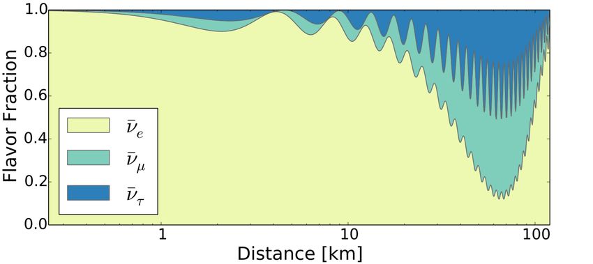
range of the dynode skip distribution is at greatest risk of being lost below the
charge trigger threshold. This would degrade the detectors and must therefore be
prevented if possible.
    Parameter minimization is what allows the various models to be judged quanti-
tatively against the reference data. Various concepts and techniques are discussed,
such as stochastic fluctuations, goodness-of-fit using a modified least squares tech-
nique, and oversampling. Following that is a discussion about the various merits
and drawbacks of two popular minimizers from Root’s Minuit package, Migrad and
Simplex [13]. This discussion also features an investigation into the retarding ef-
fects on convergence by stochastic model noise. Finally, the two leading simulation
models are compared and contrasted with the help of fake-data testing.
Chapter 2
Neutrino oscillations
The phenomenon of neutrino oscillation has no classical analogue. It is a purely
quantum mechanical result of flavor eigenstates not mapping one-to-one onto mass
eigenstates. JUNO’s main supply of neutrinos are electron-flavor antineutrinos (ν̄e )
generated during nuclear β-decay within the reactor cores of nearby nuclear power
plants. Because neutrinos have been found to possess nonzero finite mass, a neutrino
beam could vary its flavor composition as a function of distance and energy.
2.1 Survival probability and mass hierarchy
Survival probability P (ν̄e → ν̄e ) represents the likelihood that some neutrino will
still possess its original flavor after having propagated over a given distance and
at a given energy. Figure 2.1 shows results of oscillation calculations using the 3 ν
model which involves a ν̄e source beam energy of 4 MeV and values similar to global
best-estimates for the three mixing angles θ12 , θ13 , θ23 and the two mass square
differences ∆m221 , ∆m232 (see Table 2.1) [17].
Figure 2.1: Expected composition of reactor neutrino flux at 4 MeV [17].
11Parameter best-fit value 3σ
∆m221 [10−5 eV2 ] 7.37 6.93 – 7.96
∆m231(23) [10−3 eV2 ] 2.56 (2.54) 2.45 – 2.69 (2.42 – 2.66)
sin2 θ12 0.297 0.250 – 0.354
sin2 θ23 , ∆m231(32) > 0 0.425 0.381 – 0.615
sin2 θ23 , ∆m232(31) < 0 0.589 0.384 – 0.636
sin2 θ13 , ∆m231(32) > 0 0.0215 0.0190 – 0.0240
sin2 θ13 , ∆m232(31) < 0 0.0216 0.0190 – 0.0242
δ/π 1.38 (1.31) 2 σ: 1.0 – 1.9 (0.92 – 1.88)
Table 2.1: 3-neutrino oscillation parameters, global fit. Values are for normal (in-
verted) mass hierarchy (see Figure 2.2) [16].
Figure 2.2: Neutrino mass hierarchy patterns: normal vs. inverted. Mass eigenstates
are indexed numerically, while flavor eigenstates are indexed e, µ, τ (image adapted
from [3]).Chapter 3
JUNO project
3.1 Collaboration
The JUNO collaboration encompasses over 70 institutes from around the globe.
Major milestones on the project timeline include the following:
• 2014: The JUNO collaboration was officially formed.
• 2015: Civil construction began and is still underway.
• 2019: Detector installation.
• 2020/21: Liquid scintillator installation and detector commissioning.
3.2 Physics program
The main goal of JUNO’s physics program to pin down the neutrino mass hierarchy
to 3 σ confidence within ∼ 6 years of data taking (see Figure 3.1). A secondary
goal is to measure the neutrino mixing parameters sin2 θ12 , ∆m221 , and ∆m2ee to
within 1 % uncertainty; these are currently known to precisions of just 4.1 %, 2.3 %,
and 1.6 %, respectively. Various interesting developments are also expected in the
fields of astroparticle physics, solar- atmospheric- or geo-neutrinos, nucleon decay,
or indirect dark matter searches. [15].
3.3 Detector
The Jiangmen Underground Neutrino Observatory (JUNO) is a reactor neutrino de-
tector presently being built in coastal southern China (see maps in Figure 3.2). The
main experimental hall is situated under a 700 m thick overburden of mostly granitic
stone in order to help shield against the large background of atmospheric muons (see
Figure 3.3). The detector is sited an optimal mean distance of ∼ 53 km from two
nuclear power plants at Taishan and Yangjiang, which will together eventually host
10 reactor cores generating a total of 36 GWth .
The symmetry and scale of this reactor/detector arrangement have been delib-
erately chosen so as to maximize sensitivity of reactor antineutrinos to the mass
hierarchy; in other words, the goal is to minimize the original flavor state’s survival
probability upon arrival at the detector site. Surviving electron antineutrinos are
13Figure 3.1: Pre-JUNO simulated e+ spectrum of IBDs from a reactor ν̄ idealized
experiment using a 20 kton detector with a 40 GWth reactor 58 km away [18].
expected to be detected at a rate of roughly 83/day via the inverse beta decay (IBD)
reaction ν̄e + p → n + e+ (see Figure 3.4).
The IBD cross-section is greatest between 3 − 5 MeV; also, IBD backgrounds are
relatively easily rejected. These factors make IBD the go-to channel for detecting
reactor neutrinos with a hydrogen-rich liquid scintillator. Event rate is ∼ 1 per
ton · GWth · day at a distance of 1 km from the reactor [20].
The central detector (see Figure 3.5) is a 35.4 m acrylic sphere housing 20 ktons
of linear alkyl benzene (LAB) scintillator pdoped with the fluor PPO and wavelength
shifter bis-MSB. An unprecedented 3 %/ E (MeV) at 1 MeV energy resolution is
made possible by a combination of important factors including a light yield of 1200
photo-electrons (PE) per MeV due to both high scintillator transparency at the
shifted wavelength and high optical coverage. These all represent improvements
over liquid scintillator experiments like Daya Bay, Borexino, and KamLAND [3].
The scintillator sphere is itself submerged in a cylindrical water pool which will
operate as both a Cherenkov muon veto and also as a shield against ambient radia-
tion. A muon tracker sits just above the water pool.Figure 3.2: JUNO regional map [1, 2, 3, 4]. Both Taishan and Yangjiang nuclear power plant sit ∼ 53 km from the JUNO detector.
Figure 3.3: Civil construction schematic for subterranean portion of JUNO [from
internal communication]

             Figure 3.4: IBD diagram and measured spectrum [17].
Figure 3.5: Diagram of JUNO detector [15]
Chapter 4

Hamamatsu large-area dynode
PMT

PMTs are a type of photodetector suited to very low-light applications such as
scintillator-based particle physics experiments. Indeed, PMT are considered to
be critical components of JUNO [9], which will employ dynode-based Hamamatsu
PMTs as photon detectors for both the main scintillator sphere and also the outer
water Cherenkov pool.
     JUNO has two PMT systems to detect scintillator light. There is a large-PMT
system composed of 18,000 20-inch units, 5000 of which are Hamamatsu dynode
PMTs. A complementary small-PMT system uses 25,000 3-inch PMTs interspersed
among the large ones. The systems deliver a combined coverage of > 78 % [15].
     In order for JUNO to achieve the very challenging required energy resolution
of 3 % at 1 MeV, the collaboration must maximize both the PMT photon detection
efficiency and the inward-looking photocathode coverage of the detector surface [9]
(p.156).

4.1      Dynode PMT design & function
PMTs convert incident photons into an output electrical pulse whose current is
measured. JUNO’s Hamamatsu PMTs are constructed from evacuated glass tubes
consisting of a forward-facing bell which necks down to the rear where it sockets
into its base (see Figures 4.1, 4.2). The inner surface of the bell is coated with
a thin metallic layer which functions as a photocathode. It is here that incoming
photons, having penetrated the glass, have the opportunity to liberate a PE from
the photocathode via the photoelectric effect.
     Single photons are easily detected but by themselves generate a very weak sig-
nal. In practice, the PE must undergo amplification in order for its signal to be
efficiently discernible from noise. For dynode-based PMTs this amplification occurs
as the electron number becomes multiplied by the process of secondary emission.
Specifically, an electron striking a metallic object with sufficient kinetic energy can
kick off multiple electrons from the metal’s surface. A series of these so-called dyn-
odes are staged within the PMT and held at a staggered series of potentials. The
strength of these potentials is controlled by a voltage divider circuit (the “base”)

                                          19
Figure 4.1: PMTs [5] Figure 4.2: 20” PMT socketing into base at container-testing facility near JUNO
Figure 4.3: Simplified layout of a dynode-based PMT [5]

into which the PMT sockets (see Figure 4.3).
    With proper shielding and suitably shaped electric fields, a PE can be guided
with focusing electrodes while being accelerated into the first dynode in order to
impact and produce several electrons by secondary emission. All these electrons are
then guided toward the next dynode, where most of them impact again and further
amplify the signal. This step repeats as many times as there are remaining dynodes.
The charge cascade is finally guided toward and collected by the anode.
Chapter 5
Data measurement and processing
Development of PMT charge-response models requires frequent validation against
real measured data. Direct comparison of PMT response simulation versus reality
is most easily made using charge spectra, identically-binned histograms of large sets
of charge responses.
5.1 Motivation to generate charge spectra
Generation of this type of charge spectrum from raw data requires no knowledge
of timing, which makes the simulation effort much less difficult. Sufficient statistics
must also be considered; the charge spectra used in this research are each composed
of data points from 800,000 events which may be evaluated using poisson/counting
statistics. It is for these reasons that a charge spectrum is a popular investigatory
format.
5.2 Experimental setup and DAQ
This section offers an introduction to the major components of the experimental
setup (see Figure 5.1).
5.2.1 PMT
A 20-inch Hamamatsu PMT (R12860 HQE) was employed in order to find its charge
response to incident photons. The PMT sockets into a base which houses the voltage
divider. See Appendix D for the full base diagram.
Important note for future work: the author has just discovered a pre-existing
typo in the simulation code setting resistance between HV ground and the first
dynode to 2.24 MΩ instead of the physically correct 3.24 MΩ. This could have
caused chronic underestimation of charge multiplication at the first dynode, plus
other undesirable effects.
23Figure 5.1: Experimental setup [6]
5.2.2 Lightproofing
In order to not dangerously overwhelm the PMT with ambient light, it was kept
in a light-tight “darkbox” whenever powered by high voltage (HV). A light-tight
shipping container in turn isolates the darkbox from most remaining ambient light
(see Figure 5.2).
5.2.3 Signal generator & light-emitting diode (LED)
The source of photons approved for measurement is a pulsed blue LED whose emis-
sions first backscatter off the interior of the darkbox before finally encountering the
PMT. The LED pulse voltage is tuned at the signal generator so that PMT PE
detection occurs for ∼ 10 % of triggered events [9] (p.200).
Note also the undesirability of significantly higher LED voltage due to the corre-
sponding increase in the ratio of triggered detection events involving 3+ PEs. These
high-PE events are of little interest to this investigation due to their drastically lower
probability of falling below a trigger threshold. If one assumes the number of cre-
ated PEs per event (NPE ) follows a poisson distribution, then NPE > 2 would occur
only ∼ 0.5 % of the time [8] (see Figure 5.3). An additional motive to limit high-PE
events is that the additional photopeaks could interfere with proper estimation of
the average charge amplification, “gain”.
5.2.4 HV supply & gate/delay module
The NIM gate/delay module and separate HV supply both reside in the VME rack
positioned just outside the shipping container. The gate/delay module performs twoFigure 5.2: Container plus all exterior electronics
tasks: shortening the signal generator’s rather long trigger pulse, and also delaying
it to synchronize with the PMT output. This delay is necessary to compensate for
the extra length of cabling connecting to the LED- and PMT-output.
5.2.5 Evaluation board with analog-to-digital converter (ADC)
The trigger signal is then routed to a DRS4 evaluation board, which measures the
output signal when triggered. The analog PMT output is converted into a digital
signal which is then forwarded via USB cable to the controlling PC.
5.3 Data processing
Raw data must be processed into a format allowing for direct comparison with
simulated charge spectra.
Waveforms are acquired with a C++ program based on the sampling program
found in the DRS4 C++ library [10] (pp. 6, 16). Triggering initiates collection of
voltage measurements over a preset constant interval. Baseline correction then com-
pensates for any low-frequency noise which would, at this small timescale, manifest
as a constant-value offset. The time-integrated discrete voltages, minus any baseline
offset, give the total voltage Utotal (see Figure 5.4).
5.3.1 Charge integration
Calculation of the signal pulse’s electron number Ne− using Utotal , integration win-
dow ∆t, and ADC input impedance Z = 50 Ω is undertaken using the formula
Qtotal 1 Utotal · ∆t
Ne− = = (5.1)
e e ZFigure 5.3: Miss-rates for various NPE , with typical simulation parameters [6]
Figure 5.4: PMT signal [6]
The sampling program calculates other information as well. However, for this
research the process-of-interest is distillation of all data from a single triggered event
into a single data point Ne− which is then saved to disk. A collection of such points
can then be histogrammed together to create a PMT charge spectrum.Chapter 6
Modeling PMT charge response
6.1 Motivation
This research is intended to help develop a better understanding of the ∼ 5000
Hamamatsu 20-inch PMTs which will observe in JUNO’s central detector, as well
as its outer Cherenkov pool. The primary goal of this research is to help optimize
the PMT base through better characterization of amplification processes within the
PMT dynode cascade. A secondary motive is to gain a better understanding of the
behavior and composition of individual PMT dynodes. For example, it would be
helpful to have a clearer understanding of the relationship between individual dyn-
ode voltages and skipping-behavior of charge cascades. These models have evolved
directly from [6]. They generate a PMT charge response from first principles, from
which a charge spectrum is then histogrammed and evaluated.
6.2 Charge amplification at dynodes
6.2.1 Charge acceleration
As mentioned in the introduction to PMTs, the degree of amplification at a dynode
partly depends on the voltage between it and the previous dynode. A greater electri-
cal potential between dynodes means stronger charge acceleration and consequently
more kinetic energy available to free electrons upon impact with the next dynode.
Conveniently, the voltage ratios can themselves be directly obtained from the cir-
cuit diagram of the base. This is due to the inter-dynode voltages being proportional
to the resistors in the base.
6.2.2 Dynode coatings
Secondary emission is also a function of dynode coating material. Since dynode ma-
terial is held as a business secret, these models could possibly provide a roundabout
way to discern between materials with different secondary-emission behavior.
Since the mean electron yield (δ) as a function of accelerating voltage is un-
known, the models incorporate a simple power-law relationship serves as a reason-
able approximation up to ∼400 V [11] (6). The power-law-type behavior of these
27PMT coatings becomes clearer when δ is plotted against voltage (see Figure 6.1) [7]
(p.18).
Figure 6.1: Secondary emission ratio for assorted dynode coatings [7]
6.3 Model fit-parameters
The PMT models incorporate five primary parameters: nWidth, Gain, RPE, Dyn-
Exp, and PSkip. The important task of fitting these parameters is discussed in detail
in the next chapter. The following descriptions define the five fit-parameters, de-
scribe their influence on the charge spectrum, and state their connection to physical
phenomena:
6.3.1 nWidth
nWidth represents the width of the charge spectrum’s noise peak. While using the
DRS4 evaluation board as analog-to-digital converter ADC, nWidth is dominated
by (and indeed only marginally broader than the noise peak width itself) [6].
6.3.2 Gain
Gain represents PMT total mean charge amplification for a single PE. Gain may
be visualized on a charge spectrum as the difference in electron count between thenoise peak and the 1 PE peak. Gain-value is most directly controlled by the level of the PMT’s HV supply. Refer to Appendix A for further details. 6.3.3 RPE RPE represents the average PE rate. RPE is simply the ratio of events for which the PMT detects ≥ 1 PE versus 0 PE. RPE is controlled in the lab by modulating the LED voltage. RPE is held near 0.1 for reasons previously mentioned in the LED discussion from the previous chapter. 6.3.4 DynExp DynExp represents the dynode secondary emission factor. DynExp is also related to charge amplification. DynExp’s value is bestowed by whichever yet-unidentified coating has been applied to the PMT dynodes. Higher values of DynExp correspond to higher electron count values for any given feature of the charge spectrum. 6.3.5 PSkip Finally PSkip, in its various forms, represents the probability that electrons skip a dynode. PSkip manifests itself in the charge spectrum as the skip-peaks which occur at lower yet still partially overlapping charge-values (due to hitting fewer total dynodes) than their corresponding photo-electron peaks. PSkip’s values arise primarily from a combination of PMT geometry and magnetic fields; PSkip values are therefore sensitive to charge deflection from unshielded external magnetic fields, e.g. Earth’s. Higher PSkip values amplify skip peaks at the expense of a diminished amplitude for the corresponding PE peak. See Appendix B for further discussion. 6.4 Peaks within valleys The section greatest interest within the charge spectrum is the “valley” of inter- mediate Ne− values between the noise peak (pure-noise spectrum, as if the PMT provided no output) and the 1 PE peak. This valley, in addition to the flanks on either side, is home to most of the charge-signals resulting from ≥ 1 dynode skips during PMT signal amplification (see Figure 6.2).
Figure 6.2: Charge spectrum: contributions to the valley (circled) are of primary
interest.
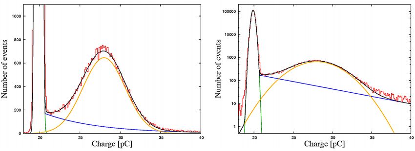
Prior models have treated these skip-peaks as background that decreases expo-
nentially with increasing charge count [8] (p.8) & [12] (3.1–3.5). For example, in
Figure 6.3 the charge spectrum raw data is modeled as the sum of gaussian curves for
both noise peak and 1 PE peak (green and orange, respectively) plus an exponential
curve (blue) to fudge the difference.
This work further develops Figure 6.3’s nonphysical exponential curve (blue-
colored) into Figure 7.6’s two skip-peaks (violet and light blue-colored), which are
instead generated from first principles and deliver better agreement with measured
data.
Figure 6.3: Previous, cruder method for fitting a PMT charge spectrum [8]
6.4.1 Peak-to-valley ratio
The peak-to-valley ratio P/V is a unitless value describing the height of a charge
spectrum’s photopeak relative to that of the valley. A quick look at Figure 6.3reveals P/V ≈ 700/200 = 3.5.
P/V is also conceptually related to energy resolution. For example, the charge
produced by a PE is influenced by processes independent of the visible energy, which
further blurs the charge spectrum. The result is that some PEs undergo lower-than-
normal amplification and become hidden beneath the noise peak. This process
degrades resolution in a manner strongly dependent on P/V [9] (p.195).
6.4.2 Direct triggering and PMT efficiency
JUNO’s operational mode involves direct triggering on PMT signals. A charge
threshold must therefore be assigned, whereby only signals above the threshold are
defined as valid triggers. Signals generated by PEs which have skipped the very
first dynode are at greatest risk of falling below a trigger threshold, as these signals
tend to have the lowest gain among all 1 PE skip peaks. See Appendix B for further
discussion.
6.5 Simulation walkthrough
The running simulation passes through three main stages which are presented here
chronologically and finally condensed into a single flowchart:
• Stage I deals with PE generation.
• Stage II handles processes within the dynode array like secondary emission
and dynode skips.
• Stage III adds noise to the signal.
6.5.1 Simulation stage I
Figure 6.4: Simulation stage I [6]PE production-probability follows a poisson distribution:
RPENPE −RPE
P (NPE ) = e (6.1)
NPE !
RPE therefore corresponds to the fraction of 1 PE events out of all events.
6.5.2 Simulation stage II
Figure 6.5: Simulation stage II [6]
PEs, once produced, then begin to pass through the dynode array.
Secondary e− production
Models of secondary emission also follows a poisson distribution. The expectation
value is now the mean electron yield δ̄ (δi from equation (9.2)). The probability at
a dynode of the production of δ secondary electrons is now given by
δ
δ̄ −δ̄
P (δ) = e (6.2)
δ!
A computationally quicker approximation is used if δ̄ ≥ 50, whereby the prob-
√ function of a normally distributed random variable (mean µ = δ̄,
ability density
width σ = δ̄) is adopted for simplicity:
2 !
1 1 δ − δ̄
P (δ) = √ exp − (6.3)
2π δ̄ 2 δ̄
This is helpful because of the relative ease with which a single normally-distributed
random value is chosen, as opposed to the computationally expensive task of sum-
ming over many poisson-distributed random values.Dynode skips
Dynode skips are decided upon the arrival of charge at each dynode; skips occur
whenever a dynode’s PSkip value is found to be greater than a random value selected
from a flat distribution between 0 and 1.
6.5.3 Simulation stage III
Figure 6.6: Simulation stage III [6]
Finally, random fluctuations following a normal distribution are added to better
simulate noise contributions from ADC and also to a lesser extent from the PMT.
6.5.4 Comprehensive flow chart
All three simulation phases are summarized in Figure 6.7. Visualizations of simula-
tion output are provided in the next chapter.
Figure 6.7: Simulation overview including dynode skip probabilities [6]Chapter 7
Parameter minimization
Parameter minimization is what allows the various models to be judged quantita-
tively against the reference data. First, some various concepts and techniques are
discussed such as stochastic fluctuations, a modified least-squares technique, and
oversampling. Following that is a discussion focusing on two popular minimizers
from Root’s Minuit package [13], Migrad and Simplex.
7.1 Concepts & techniques
7.1.1 Stochastic fluctuations
Much of the minimization challenge revolves around finding working strategies for
dealing with impractically large statistical fluctuations. These stochastic fluctu-
ations have been baked into the simulation in many ways. While this has been
necessary for generating realistic simulations, unfortunately it also amplifies the
challenges involved in coaxing a gradient-method minimizer, such as Migrad from
Root’s Minuit package, to converge.
7.1.2 Goodness-of-fit
χ2 is the standard tool with which to test gaussian data for goodness-of-fit. χ2
should ideally be a value near 1 after having been divided by the number of degrees
of freedom (NDF). χ2 /NDF values
1 imply that the model does not properly
describe the measured data, whereas values
1 hint at error overestimation of
gaussians associated with the simulated data [19].
For this research, all quantitative comparisons of data versus simulation are
computed using a modified least-squares method
2
X (data − simulation)2
χ = p 2 (7.1)
bins dataError2 + simError2
whose output includes an additional contribution, from the simulation of statisti-
cal/counting error, added to the denominator in quadrature.
35The counting error associated with each bin of the charge spectrum is poissonian
in nature and therefore grows as the square root of the number of counts in a given
bin. This means that, on average, the acquisition of more real data or the generation
of more simulation data will result in a preferentially lower noise-to-signal ratio per
bin.
The χ2 value may be compared directly to that of other models when divided
by the number of degrees of freedom (NDF), which is the number of histogram bins
within the evaluation range minus the number of free parameters in the model.
7.1.3 Oversampling
“Oversampling” is here defined as simulation generation involving more events than
its respective measured dataset [6]. For example, a comparatively higher oversam-
pling factor (oF) appears to smoothen stochastic noise in scan-parabolas (see Figures
7.1 and 7.2).
Oversampling is additionally helpful in the sense that it helps prevent the fit-
ter from being fooled by local minima representing purely statistical fluctuations.
Convergence to these local minima would be counterproductive to the minimizer’s
efforts to find a legitimate and preferably global minimum.
7.2 Migrad minimizer
Minuit’s default gradient-based minimizer is Migrad, which properly converges onto
solutions in order to provide meaningful information about parameter values and
their uncertainties.
“Fake data” was used during the vast majority of efforts to discover Migrad’s
reluctance to converge. As opposed to “real” measured data, fake data presents an
information environment featuring fewer unknown variables/influences.
7.2.1 Coaxing convergence
Two complementary strategies exist for aiding minimizer convergence:
Strategy 1
The first strategy addresses simulations’ influence in the denominator of χ2 calcula-
tions via the simError term from equation (7.1). Figure 7.1 shows parameter scans
taken about the true value for various levels of simulation-oversampling. Note how
higher OFs smooth out stochastic noise and reveal the underlying parabolic struc-
ture. This enables Migrad to more reliably seek the true parameter value presumably
lurking at the parabola minimum.Figure 7.1: Smoothing effect of higher simulation oversampling factors
Strategy 2
The second strategy focuses on measured data’s influence in the denominator of
χ2 calculations via the dataError term from equation (7.1). For χ2 minimization,
capturing more real data results in much higher-than-otherwise χ2 values for non-
optimal parameter values.
A parameter scan about some best-value would visualize this as a parabola whose
slope grows more steeply than otherwise whenever one moves away from the best-
value. The increased steepness of these sidewalls is certainly a positive trait because
for any given amplitude of statistical fluctuation, the risk of Migrad stumbling into
and becoming trapped by false minima is confined to a narrower “well” which occu-
pies a smaller range about the truly best value.
Figure 7.2 demonstrates the comparative benefits of more fake data. Both plots
display parameter scans about the same range in the vicinity of the parameter’s
true value. Compare the curves in both plots with OF held constant and > 1:
increasing data by factor 10 better reveals the parabola’s curvature, a phenomenon
which should be helpful to Migrad.Figure 7.2: The benefits of more measured data
These various minimization strategies would presently likely require simulation
OFs of many hundreds in order to properly converge. A few constraints bear men-
tioning:• Oversampling factors of this magnitude are presently restricted by computing
challenges involving memory over-allocation.
• All minimization strategies require the simulation to be re-run once per it-
eration with freshly updated input parameters, which means that every fit
invokes hundreds of unique (although optionally repeatable) simulations.
7.2.2 Pull
Pull was recruited as a tool to help evaluate two extreme examples of scan-values (see
Figure 7.3). The main purpose of these evaluations was to determine whether such
extreme fluctuations were statistically-driven or simply bugs arising from something
else, for example poor modeling assumption or false uncertainty estimation.
Pull is defined [14] here as the distribution
simi − datai
(7.2)
σi
where “data” is the per-bin value of a charge spectrum generated from fake-data,
“sim” is the per-bin value of a simulation, and σ is the expected uncertainty (see
Figure 7.4). The high oversampling factor was chosen to render sim’s counting-error
negligible compared to data counting-error.
Figure 7.3: Extreme examples of stochastic noise obscuring the minimum of a scan-
parabolaSim’s parameters were held to true fake-data values, excepting of course the
scan-parameter itself (here Gain).
σ is the error-propagated uncertainty of the pull-formula’s numerator; that is, σ is
the counting error of both simulation and data having been added in quadrature. An
ideally simple and well-behaved pull manifests as a standard gaussian distribution
with width 1, mean 0, and no long tails. Even if long tails are present, 1 σ error
analysis remains valid [14].
From Figure 7.4 one may conclude, due to the decent agreement with gaussians
fit to the distributions for the two scan-values, that the extremely jagged fluctuations
seen in Figure 7.3 are purely stochastic.
Figure 7.4: Pull distributions: an investigation into the extreme scan-values from
Figure 7.3
One may also infer from Figure 7.4’s fit-widths (∼ 1 and ∼ 1.3, respectively)
that the average fit-width is somewhat larger than the ideal value of 1. This is
symptomatic of error underestimation.
7.3 Simplex pseudo-minimizer
Minuit’s simple and robust package Simplex [13] has been adopted as the most
reasonable option for progress to be made without convergence-dependence.
One major drawback is that it is unable to provide reliable error estimation.
The adopted work-around to this, as introduced in the section on fake data, is to
histogram the results from a large collection of parameter fits and then to estimate
parameter error by taking the standard deviation of the distribution (see Figure
7.5.)The algorithm to conduct these fits works as follows: each Simplex fit iterates a
preset number of times. The tolerance parameter is set low enough to prevent any
convergence, since that would in this case be counterproductive. The fit-iteration
which scores the lowest χ2 value has its parameter values written to file. The entire
process is repeated ∼ 100 times, after which the saved fit-results are histogrammed
for final evaluation.
Figure 7.5: Typical results for parameter fits to both models7.3.1 Comparison of two models
The simplest PMT model, henceforth called Model 1, employs for each of the ten
PMT dynodes a single universal dynode skip probability (see Figure 7.6).
Figure 7.6: Model 2 charge spectra: data vs. simulation seeded with best-fit param-
eters
Model 2 differs in that it employs independent per-dynode skip probabilities for
dynode groups 1, 2-5, and 6-10. Dynodes are counted upward along the path of
charge propagation.
Model 1 is the only verifiably stable model and so is treated as the default.
For further discussion about model stability, refer to the discussion of fake-data
testing. However, Model 2 is more physically realistic. This is reflected in Model
2’s stronger performance during parameter pseudo-minimization against measured
data (see Figure 7.7).Figure 7.7: Model 2 charge spectra: data vs. simulation seeded with best-fit param-
eters
The residuals plotted for each model show the per-bin difference, in units of
standard deviation, between measured and simulated charge spectra. Error is the
quadratic sum of poissonian counting error for both the measured and simulated
charge spectrum.
Greatest deviations in the residual plots of Figures 7.6 and 7.7 occur on the
negative flank of the noise peak beyond the reach of other charge contributions.
These largest residuals are likely a consequence of imperfect baseline correction of
individual charge pulses [6] (see Figure 5.4). Hence the lower bound of the χ2
evaluation range is truncated to −2 × 10⁶ e− .
The upper bound of electron counts contributing to χ2 evaluation is 40 × 106 .
This was originally chosen to avoid bins with low statistics on the high flank of the
2+PE photopeak.
Other residual-structures likely indicate anomalies such as imperfect modeling
of the PMT charge response or remnant bugs in the simulation/evaluation code.7.3.2 Fake-data testing with Simplex
Fake-data testing is here employed primarily to assess the stability of the Simplex
parameter pseudo-minimization algorithm.
Instead of beginning with a physical measurement, the simulator is run with pa-
rameters set to nice round “true” values for ease of analysis. The pseudo-minimizer
is then fed the fake-data as if it were real data, and after the proper resetting of the
algorithm’s seed- and step-values, the pseudo-minimizer attempts to rediscover the
true parameter values.
Figure 7.8 displays the histogrammed results of ∼100 of these fits to fake-data
for both Model 1 and Model 2. Note how the fitter finds nWidth, Gain, and RPE
with relative ease, while the true values of DynExp and PSkip prove rather more
elusive.
The standard deviations of the histogrammed distributions in Figure 7.8 serve
as a best-estimate for error on these parameter values, since the Simplex-based algo-
rithm does not support gradient-based methods of proper parameter minimization
with proper convergence (see section on parameter fitting without convergence).Figure 7.8: Typical fake-data results for parameter-fits to both models
Also notable is the fitter’s generally poorer performance when dealing with Model
2 (see Table 7.1, 7.2). This is partly due to the substitution of a single relatively
stable fit-parameter (the universal skip probability PSkip) with three comparatively
less-influential (although probably more realistic) dynode skip parameters.
Simplex pseudo-minimization of any model requires careful choice of fit-parameter
seed values. This has been most apparent when working with the more difficult-
to-find parameters DynExp and PSkip(s). Additional care must be taken when
choosing pseudo-minimizer step values, since one must of course compromise be-
tween coverage of a sufficiently large parameter space versus wielding a fine enough
resolution to detect relatively narrow features.Model 1 parameter Mean fit-value True value (exact)
nWidth (1.003 ± 0.003) × 106 1 × 10⁶
Gain (1.50 ± 0.01) × 107 1.5 × 10⁷
RPE 0.100 ± 0.001 0.1
DynExp 0.77 ± 0.02 0.8
PSkip, universal 0.028 ± 0.002 0.03
Table 7.1: Fake-data parameter fits for Model 1
-------------------------------------------
Model 2 parameter Mean fit-value True value (exact)
nWidth (1.000 ± 0.003) × 106 1 × 10⁶
Gain (1.48 ± 0.01) × 107 1.5 × 10⁷
RPE 0.101 ± 0.001 0.1
DynExp 0.75 ± 0.03 0.8
P1Skip 0.05 ± 0.01 0.03
P(2-5)Skip 0.017 ± 0.002 0.02
P(6-10)Skip 0.034 ± 0.003 0.04
Table 7.2: Fake-data parameter fits for Model 2
Both of these models represent real progress toward a better understanding of
charge generation within large-area dynode PMTs.Chapter 8
Summary and outlook
Summary
Development of PMT charge-response models requires frequent validation against
real measured data. Charge spectra histogrammed from the integrated charge of
single events are the preferred format for direct comparison between simulated and
measured data.
Parameter minimization is what allows the various models to be judged quantita-
tively against the reference data. Various concepts and techniques such as stochastic
fluctuations, goodness-of-fit using a modified least squares technique, and oversam-
pling were discussed.
Next, two popular minimizers from Root’s Minuit package, Migrad and Sim-
plex [13], were compared; followed by an investigation into the retarding effects
on convergence by stochastic model noise. Migrad, when it is finally coaxed into
convergence by clever tricks and brute-force computing, could provide a desirable
gradient-based parameter minimization method complete with covariance matrix.
Meanwhile, the Simplex pseudo-minimizer has successfully served as a stop-gap so-
lution and performs quite satisfactorily for the relatively simple models developed
thus far.
Fake data
Simplex and fake-data testing allowed for direct comparison of the fit-stability of
the two main PMT charge generation models (see again Figure 7.8 and Tables 7.1
& 7.2):
1. Model 1, featuring a universal dynode skip probability, delivered fake-data fits
whose values remained within ∼ 1.5 σ for every parameter. Simplex fits to
Model 1 work quite well.
2. Model 2, featuring multiple dynode skip probabilities, proved a bit more diffi-
cult to handle. Fake-data fits to Model 2 were less accurate but still generally
successful, returning all parameter values within ∼ 2 σ of true value. Relative
to Model 1, mean fit-values differed more from true values and also varied
more from fit to fit. However, Model 2 also tended to perform better during
χ2 goodness-of-fit analysis; it seems to be the more physically realistic model.
47Model 2 also has more potential for future improvement and is expected to
ultimately prove itself the better model.
Real data
Simplex pseudo-minimization to real data (see again Figure 7.5) revealed that the
models agree nicely for parameters nWidth and RPE, although for Gain and DynExp
one sees only a small fraction of overlap on the fit-histograms.
For DynExp, three different fit-values may be compared: Model 1 (0.81 ± 0.02),
Model 2 (0.86 ± 0.02), and the independently-determined power law fit to Gain-vs.-
HV data from Figure 9.1 (0.603 ± 0.002). There is clearly disagreement here but no
good way at present to know which if any is correct because the true PMT DynExp
value remains unknown.
Last up is PSkip. Model 1’s pseudo-minimization of real PMT data returned
a universal skip probability best-estimate of (2.3 ± 0.2) %, which seems plausible.
Model 2 returned skip probabilities of (3.2 ± 0.6) %, (1.5 ± 0.2) %, and (3.7 ± 0.3) %
for dynode(s) 1, 2-5, and 6-10, respectively. This seems plausible as well, although
fits to these parameters are the most sensitive to choice of pseudo-minimizer seed
value and step size.
In conclusion, both models represent good progress toward building a useful
statistical model of charge generation within large-area dynode PMTs.
Outlook
Many next-steps exist for research into charge generation of large-area dynode PMTs.
For example, the DRS4 evaluation board has since been replaced by an ADC which
should generate a much narrower charge spectrum noise peak. This should offer the
following benefits:
• Higher P/V ratio.
• Diminished charge-blurring for all events collected in charge spectrum vis-a-vis
simulation Stage III (see chapter “Modeling PMT charge response”), possibly
revealing sharper spectral features.
• Convergence more easily achieved during parameter minimization for any
model. Among the various fit-parameters, the search for dynode skip proba-
bilities stand to benefit the most from a narrower noise peak.
• More realistic comparison to JUNO’s actual ADCs.
Also, more computing power would augment any brute-force methods of model
parameter minimization. One could generate more events per simulation, run more
total simulations, or scan parameter spaces in finer detail. Thirdly, one could learn
more about the mean electron yield δ̄ of the final dynode by measuring PMT signals
directly from the final dynode and comparing the gain to that of normal anode-based
measurements. Finally, more information than just integrated-charge is extracted
from raw PMT-response waveforms; these extra data products could be helpful in
future research.Chapter 9
Appendix
9.1 A: gain approximation
Let Ndyn be the number of dynodes within a PMT, U the various inter-dynode
accelerating voltages, DynExp the dynode secondary emission factor (also featuring
prominently as a minimizable fit-parameter), and R the various resistances within
the voltage divider:
Ndyn Ndyn Ndyn DynExp
Y Y DynExp Y Ri
0 0
Gain = δi ≈ (a · Ui ) = a · Utotal ·
i=1 i=1 i=1
Rtotal
Ndyn
Ndyn ·DynExp
Y Ri DynExp Ndyn ·DynExp
0
= (a · Utotal ) = (A · Utotal ) (9.1)
i=1
Rtotal
Utotal is simply the HV provided to the PMT, and both A and DynExp may be
extracted as power law fit parameters when Gain is plotted against HV (see Figure
9.1).
In addition, thanks to the direct proportionality between acceleration voltages
and resistances in the voltage divider of the base, Gain may also me approximated
by an equivalent power law in terms of R instead of U :
DynExp DynExp
δi ≈ a0 · Ui = a · Ri (9.2)
where a is determined by the gain. Assuming no correlation between dynode δ’s,
this means that one may approximate Gain as
Y Y DynExp
Gain ≈ δi ≈ a · Ri (9.3)
i i
49Figure 9.1: Measured PMT gain as function of HV, plotted log-log; reference to ideal JUNO gain at [9] (p.138)
9.2      B: PSkip’s influence on charge spectrum
Higher PSkip values amplify skip peaks at the expense of a diminished amplitude
for the corresponding PE peak. For example, consider the charge spectra in Figure
9.2. The only difference between these simulations is the skip-probability of the first
dynode. One can see from the lower-right plot that when all photo-electrons skip the
first dynode, every event’s electron count and therefore output-signal is drastically
reduced because of a missed opportunity for amplification.

      Figure 9.2: Simulation response to varying first-dynode skip probability
9.3 C: noise reduction via oversampling
The following is a derivation of how error reduction goes as the square root of the
oversampling factor. For starters, a histogram bin √ from a counting experiment is
0 0
populated by m events with poissonian error σ = m0 . Let m be the mean of x
repeated measurements (oversampling factor x) of the same setup, with mi large
enough to ensure that σ 0 ≈ σ1 ≈ · · · ≈ σx . By error propagation,
x 2 !
X ∂m
σ2 = σi2 (9.4)
i=1
∂m i
x x
1 ∂m 1
δij = x1 ,
P P
Since m = x
mi and therefore ∂mi
= x
i=1 j=1
various substitutions back into the formula for σ 2 gives
x 2 ! x
X 1 1 X 2 1 σ 02
2
σ = 2
σi = 2 σi = 2 x · σ 02 =
i=1
x x i=1 x x
Therefore, for a bin with mean value m, the oversampling-adjusted error is
σ0
σ=√ (9.5)
x1 2 3 4
9.4
Design for Hamamatsu PMT
also payed attention to reliability. BUT
PI MT180 PI MT170 PI MT10 PI MT08 0 PIPMT020 PI MT01 0
the HV capacitor is not stocked at most / COPMT18
PMT18 COPMT17
PMT17 COPMT10
PMT10 COPMT08
PMT08 COPMT02
PMT02 COPMT01
PMT01
all of the distributors
WIMA SMD PPS capacitors
A A
max. voltage pulses: 40 V/µs
1000V / 630V case: 5040
COPMT20 COPMT19 COPMT09 COPMT16 COPMT03 COPMT15 COPMT04 COPMT14 COPMT05 COPMT13 COPMT06 COPMT12 COPMT07 COPMT1 Voltages
PMT20
PMT19
PMT09
PMT16
PMT03
PMT15
PMT04
PMT14
PMT05
PMT13
PMT06
PMT12
PMT07
PMT11
PIPMT20 0 PI MT190 PI MT09 0 PIPMT160 PI MT03 0 PI MT150 PI MT04 0 PI MT140 PI MT05 0 PIPMT130 PI MT06 0 PI MT120 PI MT07 0 PI MT1 0
NLHVanP
HVanP
NLHVdyn08P NLHVdyn09P NLHVdyn10P
HVdyn08P
HVdyn09P
HVdyn10P
PIR102 PIR202 PIR402 PIR502
Multiple Resistors to reduce COR1
R1 COR2
R2 COR4
R4 COR5
R5
voltage drop per resistor 100 100 100 100
COR1a COR1b COR1c
PIR101 PIR201 PIR401 PIR501
R1a R1b R1c
PIR1a01 PIR1a02 PIR1b01 PIR1b02 PIR1c01 PIR1c02
560k 560k 560k
NLHVR1R2
HVR1R2 NLHVdyn01 NLHVdynF NLHVdyn02 NLHVdyn03 NLHVdyn04 NLHVdyn05 NLHVdyn06 NLHVdyn07 NLHVdyn08 NLHVdyn09 NLHVdyn10
HVdyn01
HVdynF
HVdyn02
HVdyn03
HVdyn04
HVdyn05
HVdyn06
HVdyn07
HVdyn08
HVdyn09
HVdyn10
COR2a
R2a COR2b
R2b COR2c
R2c COR3
R3 COR7
R7 COR8
R8 COR9
R9 COR10
R10 COR11
R11 COR12
R12 COR13
R13 COR16
R16 NLHVan
HVan
PIR2a01 PIR2a02 PIR2b01 PIR2b02 PIR2c01 PIR2c02 PIR301 PIR302 PIR701 PIR702 PIR801 PIR802 PIR901 PIR902 PIR1001 PIR1002 PIR1101 PIR1102 PIR1201 PIR1202 PIR1301 PIR1302 PIR1601 PIR1602
B 560k 560k 560k 180k 620k 300k 300k 300k 300k 300k 300k 10k B
PIR4a02 PIR5a02 PIR6a02
COR4a
R4a COR5a
R5a COR6a
R6a COC1
C1 COC2
C2 COC3
C3 COC4
C4
560k 560k 430k V(R10) = 100V PIC101 PIC102 PIC201 PIC202 PIC301 PIC302 PIC401 PIC402
WIMA SMD PPS 10nF 1000VDC
PIR4a01 COR4b
R4b
PIR5a01 COR5b
R5b
PIR6a01 COR6b
R6b
HVGND PIR4b02 PIR4b01 PIR5b02 PIR5b01 PIR6b02 PIR6b01
470k 560k 470k COC1a
C1a COC2a
C2a COC3a
C3a COC4a
C4a
PIC1a01 PIC1a02 PIC2a01 PIC2a02 PIC3a01 PIC3a02 PIC4a01 PIC4a02
10nF 250V 10nF 250V 10nF 250V 10nF 250V
COC5
C5
Reliability Estimate: PIC501 PIC502
NLHVpmt0
HVpmt0
VISHAY CRCWe3 26 x 0.1 = 2.6
Connections to GCU WIMA capacitors 10n 4 x 2 = 8 HFE472MBFEJ0K Vmax = 3kV
VISHAY HFE : 2 x 5 = 10 HVGND 4n7 6kV OverVoltageProtection
FIT 5E-9 OverVoltageProtection.SchDoc
COCon1
Total FIT: 20.6 + PCB PIR1902 ADC_IN
ADC OUT PMT Anode
Con1 NLADC0OSC
ADC_OSC 24V0 COR19
R19 ADC_OSC
PICon100 ADC OSC
COHV3
HV3 10k
C COCon2
Con2 C
PICon200 PIHV304
4 PIR1901
HVGND 24V
1
PIHV301
COCon3
Con3 NLADC0IN GND
ADC_IN
PICon300
2
PIHV302 GND NLHVout
3
PIHV303
10
PIHV3010
HVout
GND HVout
GND U_nom = 2000V
HV_ISO_VCC 5
PIHV305 5Vout
24V0
COP1
P1 8
HV_LAM PIHV308 9 COR17
R17
LAM HVrtn PIHV309 PIR1701 PIR1702
PIP101
HV_RS485_A 6 0R
1 PIHV306 A
PIP102
HV_RS485_B 7
2 PIHV307 B
HVGND GND
HV Module
COCon4
Con4 NLHV0RS4850B
HV_RS485_B GND Isolation Distances
PICon400
http://www.elektronikpraxis.vogel.de/index.cfm?pid=11180&pk=449558&type=article&fk=356703
COCon5
Con5 NLHV0RS4850A
HV_RS485_A COCon8
Con8NLHV0ISO0VCC
HV_ISO_VCC
PICon500 PICon800
>500V d = 3.05µm/V 3kV = 9.15mm
COCon7
Con7 NLHV0LAM
HV_LAM COCon6
Con6 2kV = 6.1mm
PICon700 PICon600
D Variant: Production D
GND
Normal Hamamatsu Base: Low Current Base:
Hamamatsu 20" PMT Base
D: Hamamatsu 20” PMT base diagram
Total resistance: 4.51 MOhm Total resistance: 27.67 MOhm
Revision: 1
Divider current: 554 µA @ +2500V Divider current: 90 µA @ +2500V Internal connected pins Author: Jochen Steinmann 422
"inspired" from A. Garfagnini (JUNO docDB 1174-v1) J01, J10, J08, J17, J02, J18 Date: 24.09.2018 Time: 17:29:03 Sheet 1 of 2 Otto-Blumenthal-Straße - 52074 Aachen
File: C:\Users\steinmann\Documents\Altium SVN\JUNO_HamamatsuBASE_FINAL\pmt_base.SchDoc
1 2 3 4You can also read