De la recherche fondamentale à la Start-Up - Etienne GHEERAERT CNRS,University of Grenoble - Alps and University of Tsukuba
←
→
Page content transcription
If your browser does not render page correctly, please read the page content below
De la recherche fondamentale à la Start-Up
Etienne GHEERAERT
CNRS,University of Grenoble - Alps and University of Tsukuba
                                                               1

                                      JEPHY 2018 Avignon
Contexte

     LEPES: Laboratoire Propre de Recherche Fondamentale en
                         Physique du Solide
    CNRS MPB (ancêtre INP): Mathématique et Physique de Base

                    Ion Solomon (1990):
  « Si vous ne savez pas pour quelle application vous
travaillez, alors vous travaillez à 100% pour les japonais
   et les américains, car eux l’application ils vont la
                         trouver . »

                                                               2
Contexte

 NIMS (Japon): Institut de Recherche sur la Science des
                        Matériaux

Impact du terme « Fondamental »

Innovation au coeur de la recherche

Des outils pour traverser la « vallée de la mort »

                                                          3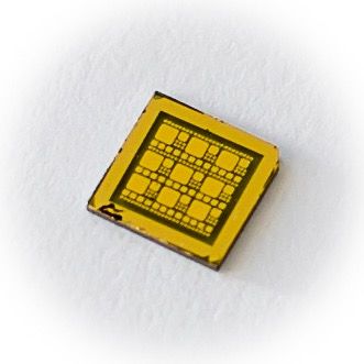
Contexte: NEEL group
                     Wide Bandgap Semiconductor Group

      Understand                         Control                                 Innovative devices
          Impurity centres
                                         Epitaxial Growth               Electronic                 Bio-related
     Diamond Heterostructures
    Transport in semiconducting         In-situ monitoring             Power electronics
                                                                                                     Membranes
            nanowires                    Nano-fabrication               Nanowire LED
                                                                                                     Bio sensors
  Superconducting semiconductors      Impurity incorporation         Single photon source
         Photospintronics              Oxide gate insulators
Superconductor/Insulator Transition

ANR Transport in ZnO (Coll. Leti)                              FUI Power Schottky (Alstom)
ANR Transport in GaN (Coll. Leti)                                                                ANR JC D. Eon
                                                                LANEF PhD (Coll. G2ELab)
                                                                   LANEF Eqt CARAPACE        LANEF PhD (Coll. INAC)

                                                                                                                      4
Context: Diamond diodes
     Schottky diodes at NEEL

              Breakdown voltage: Vbreak>1000 V on
              1.3µm
              On resistance : Ron = 52 Ω (@300 K)
              Diode surface : S = 7.85 10-5 cm2.
              RonS = 4 mΩ.cm²

                             A. Traore et al APL 2014   5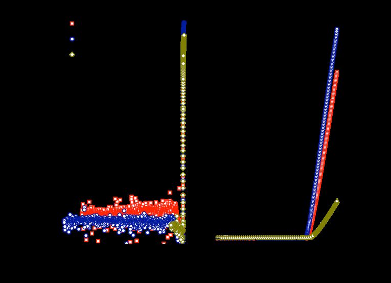
What material for power electronics ?

 Property                  Symbol            Si      4H-SiC     GaN            -Ga2 O3   Diamond
 Bandgap                   EG [eV]           1.1     3.23       3.45       4.5           5.45
 Sat. drift velocity       vS [107 cm/s]     1.0     2.0        2.2        -             1.1
 Electron mobility         µn [cm2 /V.s]     1500    1000       1250       300           1000
 Hole mobility             µp [cm2 /V.s]     480     100        200        -             2000
 Breakdown field           Em [MV/cm]        0.3     3          2          8             10
 Dielectric constant       ✏r                11.8    9.8        9          10            5.5
 Thermal conduct.               [W/cm.K]     1.5     5          1.5        0.11          22
 BFM (absolute)            [MW/cm2]          42      2⇥104      8⇥103      1.4⇥105       9.7⇥105
 BFM (relative)            [Si=1]            1       550        190        3200          23000

Table 1: Properties of main semiconductors for power electronics and the corresponding Baliga       3
                                                                                  BF M    = µ✏    E
                                                                                                 r m
Figure of Merit (BFM). For each material the most favorable carrier mobility (µn or µp ) is
used to calculate the figure of merit

required to get a 1 kV breakdown voltage, and this leads to a high resistance                           6
What material for power electronics ?
                 1,0E+00
                                                                                                      Si CoolMOS

                                                        0K
                                                                                                      Si 1D limit

                                                      30
                                       Si-IGBT               Diamond                                  SiC 1D limit

                                                   Si
                                                             Schottky                                 Diamond 1D limit
                                                                                                      Diamond Schottky
                 1,0E-01          Si-CoolMOS                                                   TO
                                                                                              G       Si IGBT
                                                                                          C
                                                                                        Si            SiC MOSFET
                                                                                                      CREE Gen3 SiC-MOS
RonS (Ohm-cm2)

                                                                                                      Cree SiC p-GTO
                                                                                                      Cree SIC n-IGBT

                 1,0E-02

                                                                                   0K
                                                                                 30
                                                                               d
                                                                             on
                                                                                         SiC

                                                                            m

                                                                          3K
                                                                                        IGBT

                                                                         ia

                                                                       52
                                                                       D

                                                                     d
                                                                   on
                 1,0E-03

                                                                  m
                                                               ia
                                                              D
                                 SiC-523K

                                 SiC-300K

                                                          SiC-MOSFET
                 1,0E-04
                           100                    1 000                       10 000
                                               Breakdown Voltage (V)
                                                                               Based on H. Umezawa calculations, AIST     7
Potential application
(6) Improving fuel efficiency 15
Silicon
SiC
Goal: 10% fuel improvement*
*Japanese JC08 test cycle
Due to the increased efficiency, Toyota is aiming for a
10% improvement in fuel efficiency
Toyota 2014 8What material for power electronics ?
EMICONDUCTOR TECHNOLOGY ROADMAP FOR POWER ELECTRONICS DEVIC
Two possible approaches within the semiconductor technology roadmap for Power Electronic devices:
• Progressive evolution
• Significant improvement (“revolution”)
Diamond
performance
performance
.
rtunities
ent to
diamond
eadily
SiC, GaN
Device
ent.
Device
.
Si
Technology and cost barriers
Executive Summary ©2016 | www.yole.fr | Diamond substrate in power electronic applications - Final report - August 29th, 2016
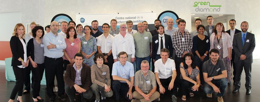
9European Project
Green Electronics with Diamond Power Devices
4 M€
2015-2019
15 partners
H2020 “Low Carbon Energy”
Coordinator: E. Gheeraert - NEEL
Kick-Off meeting, Grenoble June 2015 10Business model
Diamond
ELS OVERVIEW epitaxy provider
ess model 1: Diamond substrate supplier (epitaxy services)
Diamond
Diamond Diamond Device
device
wafer epitaxy packaging
processing
+diamond
epitaxial layer(s)
Diamond wafer The Company will realize
er(s) purchased from an epitaxial growth on a Diamond device processed and packaged by an external
external supplier purchased wafer and sell company
(Element Six, the “substrate” to a power
Sumitomo Electric…) device maker
ness model 2: Diamond bare die supplier
Diamond
Diamond Diamond Device
device
wafer epitaxy packaging
processing 11DiamFab
❖ Un CDD
❖ 3 enseignants-chercheurs
❖ PI:
❖ Savoir Faire croissance
❖ 3 brevets sur composants
❖ Soutien: SATT, French Tech
❖ Statut: Incubation
❖ Création: Automne 2018
12Conclusion
❖ Ne pas hésiter à discuter vos idées avec le SPV
❖ Breveter c’est facile (avec le SPV)
❖ Une start-up c’est une belle aventure
❖ Notre mission c’est de créer de la connaissance
❖ Notre devoir c’est d’accompagner les opportunités
de valorisation
13Thanks
Post-doc: Permanent:
M. Floren*n D. Eon
P. Thanh Toan J. Pernot
P. Muret
PhD students: H. Umezawa
K. Driche D. Chaussende
C. Masante E. Bustarret
J. Letellier
O. Loto A. Claudel
J. De Vecchy D. Barral
B. Fernandez
MSc/BSc:
C. You
F. Fillol
European Community's Horizon 2020 Programme (H2020/2014-2020)
under grant agreement n° 640947 14You can also read