Single crystal diamond pyramids for applications in nanoscale quantum sensing
←
→
Page content transcription
If your browser does not render page correctly, please read the page content below
Research Article                           Vol. 10, No. 2 / 1 February 2020 / Optical Materials Express   492

Single crystal diamond pyramids for
applications in nanoscale quantum sensing
M ARIETTA B ATZER , 1,2 B RENDAN S HIELDS , 1 E LKE N EU , 3 C LAUDIA
W IDMANN , 4 C HRISTIAN G IESE , 4 C HRISTOPH N EBEL , 4 AND PATRICK
M ALETINSKY 1,2,*
1 Department   of Physics, Klingelbergstrasse 82, University of Basel, 4056 Basel, Switzerland
2 SwissNanoscience Institute, Klingelbergstrasse 82, 4056 Basel, Switzerland
3 Universität des Saarlandes, Fakultät NT, Physik, Campus E2.6, 66123 Saarbrücken, Germany
4 Frauenhofer Institut für angewandte Festkörperphysik, Tullastrasse 72, 79108 Freiburg, Germany
* patrick.maletinsky@unibas.ch

Abstract: We present a new approach combining top down fabrication and bottom up overgrowth
to create diamond photonic nanostructures in the form of single-crystalline diamond nanopyramids.
Our approach relies on diamond nanopillars, that are overgrown with single-crystalline diamond
to form pyramidal structures oriented along crystal facets. To characterize the photonic properties
of the pyramids, color centers are created in a controlled way using ion implantation and annealing.
We find very high collection efficiency from color centers close to the pyramid apex. We further
show excellent smoothness and sharpness of our diamond pyramids with measured tip radii
on the order of 10 nm. Our results offer interesting prospects for nanoscale quantum sensing
using diamond color centers, where our diamond pyramids could be used as scanning probes
for nanoscale imaging. There, our approach would offer significant advantages compared to the
cone-shaped scanning probes which define the current state of the art.

© 2020 Optical Society of America under the terms of the OSA Open Access Publishing Agreement

Optically active point defects in solid-state hosts, also known as color-centers, form attractive,
atom-like systems, offering vast opportunities in the field of quantum science and technology.
Their spin states and optical transitions can be harnessed for applications ranging from quantum
communication [1], quantum networks [2] to quantum sensing [3,4]. The various color centers
occurring in diamond have proven particularly relevant in this development and have already
found applications in nearly all fields of quantum science and technology. Nanoscale quantum
sensors using individual, color center based electron spins in diamond have attracted particular
interest, triggered by recent success in, e.g. nanoscale imaging of superconductors [5] and
ultrathin magnets [6,7], as well as high-frequency probing of spin waves [8].
   Such nanoscale quantum sensors live up to their full potential when employed in a scanning
probe configuration using atomic force microscopy (AFM) tips decorated by single spins [3]. This
approach allows for precise, sub-nanometer positioning of the quantum sensor and thereby yields
optimized resolution and sensitivity. While early implementations of this concept have focused on
grafting color center containing nanodiamonds onto AFM tips [3,6,9], recent work increasingly
focused on “top-down” fabrication of monolithic AFM tips from high-purity, single-crystalline
diamond (SCD) [10,11]. This approach combines several advantages: It yields highly robust
tips, amenable to operation in harsh environments, such as cryogenic conditions [5]. It mitigates
optical blinking and excess spin dephasing which are both ubiquitous in nanocrystals [12]. And
lastly, it allows for tailoring the photonic properties of the tips to yield high fluorescence collection
efficiencies and thereby sensitivity [13].
   However, the same approach also comes with several drawbacks. On the one hand, the hardness
and chemical inertness of SCD requires harsh plasma etching procedures in the nanofabrication
processes, which leaves the SCD surface damaged and results in non-ideal coherence properties

#380362                                                                   https://doi.org/10.1364/OME.380362
Journal © 2020        Received 14 Oct 2019; revised 10 Dec 2019; accepted 10 Dec 2019; published 14 Jan 2020

Research Article                         Vol. 10, No. 2 / 1 February 2020 / Optical Materials Express   493

of the sensing spins [14]. On the other hand, all single color center SCD scanning probes
demonstrated up to now assume the approximate shape of a truncated cone, with a relatively
blunt, circular end-facet of ∼ 200 nm diameter. While this shape has proven beneficial for the
tips’ photonic properties [13], it is far from ideal for AFM performance for two reasons: First,
the bluntness of these tips prevents simultaneous high-resolution AFM imaging with single spin
magnetometry, which is relevant when imaging samples with non-planar geometries. Second,
pillars with circular end-facets require excellent angular alignment to be in full contact with the
sample, which typically results in increased spin-sample distances and a resulting loss in spatial
resolution and sensitivity per source strength [3].
   In this work, we present a new approach to realising all-diamond tips for scanning-probe,
nanoscale quantum sensing, which has the potential to address all the drawbacks of previous
approaches highlighted above. For this, we combine aspects of “top-down” (etching) and
“bottom-up” (overgrowth) fabrication to yield nanometer-sharp, pyramidal diamond tips, as
illustrated in Fig. 1(a). Specifically, we overgrow SCD nanopillars, fabricated via reactive ion
etching, with high purity SCD by chemical vapor deposition (CVD). The highly anisotropic CVD
growth transforms these pillars into SCD pyramids [15,16]. The pyramids show high collection
efficiencies for color center photo luminescence which together with their sharp apex radius of
curvature of ∼ 10 nm makes them perfectly amenable for future applications as scanning probes.

       Fig. 1. (a) Schematic of the nanofabrication and overgrowth processes to obtain single-
       crystal diamond (SCD) pyramids. I: Definition of etch-masks by e-beam lithography; II:
       Reactive ion etching of diamond nanopillars; III: Overgrowth of diamond material to form
       pyramids; IV: 14 N-ion implantation and annealing. (b) Scanning electron microscopy (SEM)
       image of representative diamond nanopillars after nanofabrication (step II) and (c) after
       diamond overgrowth (step III). Scalebar b  =1µm in both cases. Both SEM images were
       recorded at a 45◦ tilt angle from the sample normal. Inset: Schematic of the resulting
       pyramids with a h111i crystal facet indicated.

  To create the pillar template for overgrowth (Fig. 1(a)), we fabricated 200 nm-diameter,
cylindrical diamond nanopillars with ∼ 2µm length on a h100i-oriented electronic grade SCD
substrate grown in a custom designed ellipsoidal microwave plasma enhanced chemical vapor
deposition reactor [17]. Details of the nanofabrication process based on electron-beam lithography
and reactive ion etching have been reported elsewhere [11,18].
  The nanopillars were then overgrown by microwave plasma assisted chemical vapor deposition.
For this, an ellipsoidal microwave plasma enhanced CVD (MWPECVD) reactor was employed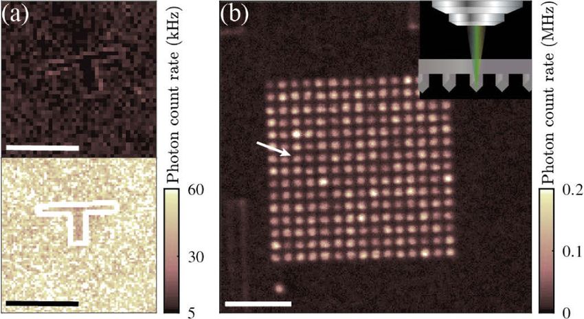
Research Article                        Vol. 10, No. 2 / 1 February 2020 / Optical Materials Express   494

[19]. The growth parameters for diamond overgrowth that led to the observed pyramid shapes
were a substrate temperature of 750◦ C, microwave power of 2.1 kW, a chamber pressure of
200 mbar and a gas mixture of 3 : 1 [CH4]:[O2] with a methane concentration of 3 % in the
process gas [19]. The flow rates for H2 and methane were 291 sccm and 9 sccm respectively.
The resulting diamond growth velocity along 100 was determined to V {100} ∼ 0.4µ/h at which
the diamond was overgrown for 75 minutes.
   As evidenced by the representative scanning electron microscopy (SEM) image shown in
Fig. 1(b), pillar overgrowth leads to the formation of pyramids with well defined geometry and
excellent uniformity across the sample. Based on the fourfold symmetry, the orientation of the
pyramids with respect to the h100i-oriented diamond surface and based on the angle between
the top facets we identify these facets as {111}-planes of the diamond crystal, consistent with
previous reports on diamond nanopillar overgrowth [16]. Remarkably, our structures exhibit
near-perfect pyramidal shape. The anisotropy of diamond growth is conveniently characterized by
the growth parameter α [20], which quantifies the diamond growth rate along the {100}-planes,
V {100} , normalized to the growth rate V {111} along the {111}-planes, i.e.
                                           √ V {100}
                                         α= 3         .                                                      (1)
                                              V {111}

Based on the observed pyramid shape, and using a recently established formalism and software
[20], we estimate α ≈ 3.1 for our diamond growth [21]. In cases, where we performed overgrowth
at different α parameters (as controlled by the substrate temperature during overgrowth [22]), or
where our starting pillars had significantly larger diameters, we observe truncated pyramids and
additional crystalline facets, consistent with previous reports [16]. The geometry of the resulting
structures as a function of initial pillar geometry and α parameter could be well reproduced by
the diamond overgrowth model and simulation by Bogatskiy et al. [20].
    To investigate the photoluminescence (PL) emitted from color centers inside the pyramids, we
employed a home-built confocal microscope [11] with numerical aperture NA 0.8 and continuous
laser excitation at 532 nm. Prior to confocal characterisation, the sample was boiled in a 1 : 1 : 1
mixture of nitric, sulfuric, and perchloric acids to remove surface residues and ensure oxygen
termination of the diamond surface. Inspection of the as-grown samples treated as described
before showed no significant fluorescence, indicating the high purity of the overgrown as well as
substrate material. After implantation (Innovion; 14 N fluence: 3e11 ions/cm2 , energy: 12 keV,
sample tilt: 7◦ ), annealing in vacuum (4 h at 400◦ C, 10 h at 800◦ C and 4 h at 1200◦ C) and a
second acid treatment, we observe significant color-center fluorescence from the diamond surface
(Fig. 2(a)(bottom)), containing spectral signatures of both negatively charged Nitrogen-Vacancy
(NV− ) and Silicon-Vacancy (SiV− ) centers, the latter of which result from Si impurities introduced
during overgrowth. Based on numerical modeling of the implantation process (SRIM software
package run with lattice binding energy 1.5 eV, surface binding energy 4.5 eV and displacement
energy 45 eV [23–25]) we expect the observed color centers to be located within ∼ 20 nm from
the diamond surface [26,27].
    For a detailed characterisation of the diamond pyramids’ photonic properties, we focused on
NV− emission and suppressed unwanted signals from SiV− emission by an appropriate short-pass
filter (Thorlabs FES0700, Cut-Off wavelength: 700 nm). A 30µm diameter gold wire loop was
positioned in close proximity to the focal spot to deliver microwave excitation to the sample. A
resulting confocal map recorded through the pyramid-base (the fluorescence collection direction
relevant for the scanning probe application we target in the future) is shown in Fig. 2(b). NV−
emission from the pyramids is significantly brighter than NV− fluorescence from the nearby
unstructured diamond, which already indicates efficient waveguiding and enhanced collection
efficiencies from these structures [28] (another potential explanation, namely the preferential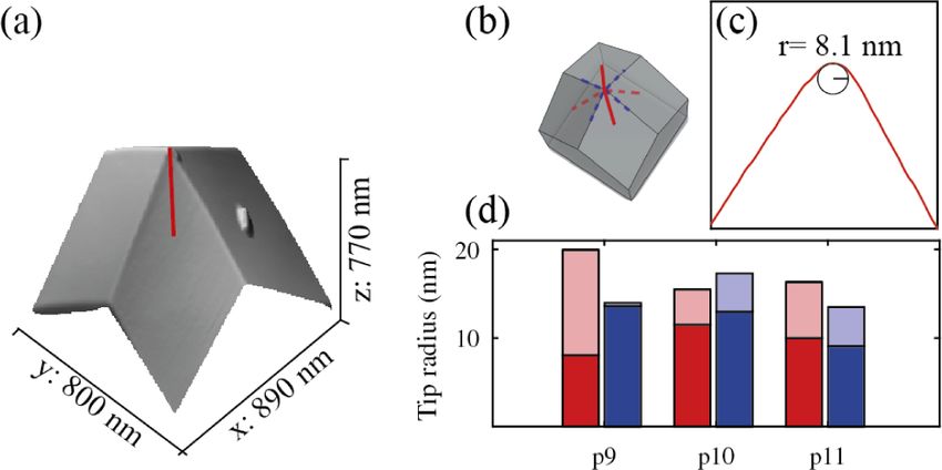
Research Article Vol. 10, No. 2 / 1 February 2020 / Optical Materials Express 495
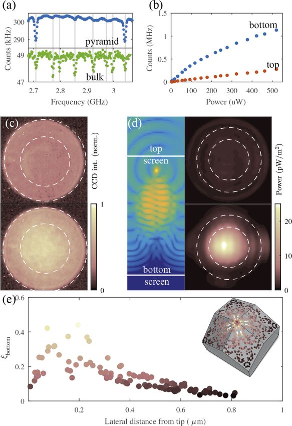
Fig. 2. (a) Confocal fluorescence map of the same part of an overgrown diamond substrate
without pyramids before (top) and after (bottom) 14 N implantation (the visible "T-shaped"
structure is an alignment marker). (b) Confocal image of an array of overgrown pyramids
with fluorescence collected for wavelengths below 700 nm. The arrow indicates the pyramid
which was further investigated in Fig. 3(a)&(b). The data were recorded using a 532 nm
excitation with 150µW and 100µW in panels (a) and (b), respectively. The scale bars
in all images is 10µm. Inset: Schematic (not to scale) of the sample orientation during
measurement. The diamond sample thickness was ∼ 20µm.
incorporation of Nitrogen into {111}-facets during diamond growth [29], can be excluded based
on the low density of residual Nitrogen (< 1 ppb [30]) in the overgrown material.
The NV− fluorescence both from the unstructured surface and from the pyramids exhibits
clear signatures of optically detected magnetic resonance (ODMR) [31]. Figure 3(a) shows two
representative ODMR traces, one from a pyramid and one from the surrounding unstructured
surface, which were obtained in the same bias magnetic field applied in a direction not aligned
with any of the diamond samples’ symmetry axes to distinguish different NV orientations.
Interestingly, the majority of pyramids investigated show a single pair of ODMR lines, whereas
the NV− ensemble observed on the unstructured part of the diamond (Fig. 3(a)) as expected
shows four such pairs, where each pair corresponds to an NV family aligned along the same,
111-equivalent crystal direction.
A statistical analysis of the number of ODMR lines observed in the pyramids allows for an
estimation of the NV density in these structures. Out of a total of seven investigated pyramids,
three showed a single pair of well resolved ODMR lines, while the remaining pyramids had either
two such pairs or unclear ODMR traces. No preferential NV orientation was observed in the
ODMR traces with a single pair of dips. Assuming a Poissonian distribution of the number of
NV’s per pyramid, the measured probability of 3/7 of observing a single ODMR line yields an
expectation value of ∼ 2.6 NVs per pillar. This estimation deviates by more than a factor of ten
from our expected NV density. Specifically, using either our implantation parameters and the
known N→NV− conversion efficiency [32] or, alternatively and consistently, the brightness of
NV− fluorescence from the unstructured surface, compared to a well-known reference sample, we
estimate an NV− density of ∼ 30µm−2 in the sample under investigation. For the given pyramid
footprint, this would result in an average number of 45 NV− centers per pyramid in stark contrast
to our above estimation. As we will show in the following, this discrepancy results from the
nanophotonic properties of the pyramids: Optical waveguiding is most efficient for NV centers
in the vicinity of the pyramid apex, and as a result, our experiment most efficiently detects NV
fluorescence from this subset of NVs only.
In order to experimentally assess the photonic properties of the nanopyramids, we measured
the angular emission patterns from their embedded NV− centers by back focal plane (BFP)Research Article Vol. 10, No. 2 / 1 February 2020 / Optical Materials Express 496 Fig. 3. (a) Representative optically detected electron spin resonance (ODMR) from a diamond nanopyramid (blue, pyramid highlighted in Fig. 2(b)) and from surrounding bulk (green). The single pair of ODMR lines indicates emission from a single or few NVs in the pyramid. (b) Fluorescence saturation curves collected from the top (red) and bottom (blue) side of the same diamond pyramid. (c) Experimentally measured back focal plane images of emission from a representative pyramid for top and bottom collection (top and bottom, respectively) (d) Finite difference time domain (FDTD) simulation of fluorescence emission from a point dipole in the overgrown diamond pyramid. Left: cross-section through the diamond pyramid with the emitter placed at the pyramid apex. Right: Simulation of far-field power distribution patterns collected from the pyramid top and bottom (top and bottom row, respectively). For all panels, white circles correspond to numerical apertures (NAs) of 0.8 and 0.5. (e) Collection efficiency for NA 0.8 through the pyramid bottom (ξ bottom ), as a function of lateral NV distance from the pyramid apex. The inset shows the NV locations considered, where the color of the points encodes the value of ξ bottom .
Research Article                         Vol. 10, No. 2 / 1 February 2020 / Optical Materials Express   497

imaging. Figure 3(c) top and bottom show, respectively, the resulting BFP emission patterns for
NV− collection through the pyramid apex (further referred to as “top-collection”) and through
the pyramid base and substrate (“bottom-collection”). In these subfigures and the following,
white circles indicate collection NA’s of 0.5 and 0.8 (the NA of our collection optics). While top
collection shows diffuse emission into the whole collection NA, bottom-collection shows a BFP
emission patterns which is more centred on the optical axis and shows emission predominantly
within a collection NA of ∼ 0.5. NV− emission from the nanopyramids shows significant
directionality: Approximately five times more fluorescence is emitted to the bottom compared to
the top side, as evidenced by both the signal integrated over the BFP images and fluorescence
saturation curves collected from the top and bottom sides for the same pyramid (Fig. 3(b)). This
observed directionality of color center emission from nanopyramids is in qualitative agreement
with previous reports [28,33].
   For a better understanding of the observed BFP emission patterns, we performed numerical
simulations using the finite-difference time-domain (FDTD) module of the commercially available
software Lumerical. There, we considered individual optical dipoles emulating NV− emission
and calculated the far-field emission patterns corresponding to our top- and bottom-collection
BFPs (Fig. 3(b), top and bottom row, respectively). The NV locations were randomly chosen on
one of the top facets of the pyramid at a depth of 20 nm below the diamond surface. To each
location, we randomly assigned one of the four possible NV orientations and performed our
calculations for two orthogonal optical dipoles lying in the plane orthogonal to the NV direction.
   The simulations qualitatively reproduce our experimental BFP images and show a clear
tendency of waveguiding of NV− emission towards the pyramid bottom. To quantify this
directionality we consider the commonly used collection factor [34]
                                                   ΓNA
                                              ξ=        ,                                                     (2)
                                                   Γrad
where Γrad is the radiative emitter decay rate in a homogeneous medium and ΓNA is the rate of
far field photons emitted into the collection NA (here with NA= 0.8). Our simulations for the
case of NV− concentration near the pyramid apex yield a top and bottom-side collection factor
ξ bottom = 0.20 and ξ top =0.058, whose ratio ξ bottom /ξ top = 3.48 is in reasonable agreement with
our experimental finding of ξ bottom /ξ top ∼ 3.2 and previous reports on similar structures [16,28].
   Our simulations also shed light on our observed discrepancy between the NV− density
estimated from the optical (ODMR) signal from the pyramids as compared to the estimated
NV− density based on implantation parameters (Fig. 3(a)). Specifically, we find that ξ bottom is
strongly dependent on the lateral NV− location within the pyramid. Figure 3(e) shows ξ bottom as
a function of this position, which we parametrize by the radial distance r of the NV− location
from the pyramid center. The simulation was performed for a selection of 110 randomly placed
NVs, where NVs with same r but different ξ bottom correspond to different azimuthal positions of
the NVs (see inset to Fig. 3(e)) and/or different dipole orientations assigned to same NV position.
The simulation shows that the NVs with the highest ξ bottom are all located close to the pyramid
apex, with ξ bottom peaking at ξmax
                                 bottom ∼ 0.5 for r ∼ 150 nm. For a qualitative estimate, we postulate

that the bottom collected NV signal be dominated by those NVs with ξ bottom > ξmax      bottom /2; from
                                                        −2
our previous NV density density estimate (∼ 30µm ), we then conclude that the emission from
∼ 3 NVs dominates the PL collected from a nanopyramid.
   We stress that further factors might add to this qualitative argument to explain the lower NV
density we observe in the nanopyramids compared to their surrounding. These include potential
distortions of electric field lines by the nanopyramids during the 14 N implantation process, which
could lead to non-uniform implantation profiles, or different degrees of incorporation of native
nitrogen or vacancies during growth of the pyramids compared the the surrounding bulk.
   One of the key benefits of working with bottom up structures is the improved surface quality
of CVD grown diamond compared to diamond etched in a plasma. To characterize and quantify
Research Article Vol. 10, No. 2 / 1 February 2020 / Optical Materials Express 498
the surface and the sharpness of our diamond pyramid tips, we performed detailed AFM imaging
on representative pyramids from our sample (Fig. 4(a)). The AFM image reflects the clear
pyramidal shape of the tip already seen in our SEM investigation and shows flat crystal facets.
The surface roughness of the pyramid facets, extracted from the AFM data in Fig. 4(a), amounts
to a root-mean-square amplitude of ∼ 0.8 nm, consistent with previous studies of diamond grown
under similar conditions [30]. More importantly though, our AFM image confirms the sharpness
of the pyramid tips already visible in Fig. 1(b). To quantify the tip sharpness, we extracted line
cuts across pyramid facets and edges as illustrated in Fig. 4(b) and fitted osculating circles to
these line profiles (Fig. 4(c)). Figure 4(d) summarizes our findings and shows the minimal and
maximal radii found in each direction for a selection of three pyramids. Importantly, all tip
radii found were in the range 8 nm · · · 20 nm, which on one hand demonstrates the remarkable
sharpness of these tips and on the other hand suggests that the values determined here are not
masked by the radius of the AFM tip employed for imaging.
Fig. 4. (a) AFM image of pyramid top facet. (b) Schematic sketch of a pyramid with
colored lines indicating the positioning of the line cuts (blue: along the edge or red: across
the facet) used to fit the tip radii in (d). (c) line cut through the AFM structure highlighted in
(a), with osculating circle fitted to the tip (black) (d) Histogram of tip radii for three different
pyramids. The darker (light) bar indicates the minimal (maximal) radii measured on each
pyramid whereas colors symbolize the direction of the line cut.
With our work we have established diamond pyramids created by CVD overgrowth of diamond
nanopillars as an attractive avenue for future all-diamond scanning probe quantum sensors.
We demonstrated a scalable process that yields sharp diamond pyramids which appear highly
attractive as robust, high-resolution AFM tips in general and for nanoscale quantum sensing in
particular. In the latter case, the sharpness of the tip would ensure close proximity of a color-center
quantum sensor placed at the apex of the pyramid to a sample of interest. An improvement over
existing approaches [10], which could promote spatial resolution in such imaging to the sub-10
nm range. Furthermore, we demonstrated that the pyramids are effective photonic nanostructures,
which yield high-efficiency fluorescence collection, on par with currently available nanoscale
quantum sensing technologies [10,35]. This, together with the native diamond surface, which
supports long spin coherence times for near-surface color center spins [36], will help further
improve sensitivities in, e.g. scanning NV magnetometry.
Two key steps still need to be addressed in order to employ such diamond pyramids for
scanning probe quantum sensing experiments: The overgrowth method demonstrated here
has to be combined with scanning probe fabrication and individual color centers need to be
controllably created at the pyramid apex. The first requirement can easily be met, since scanning
probe fabrication procedures are readily applicable to the diamond pyramids realized here.
Color-center creation at the pyramid apex appears more challenging but could be achieved by ionResearch Article Vol. 10, No. 2 / 1 February 2020 / Optical Materials Express 499
implantation with nanoscale resolution, either by nano-implantation through AFM tips [37], or
through focussed-ion beam implantation of colour centers [38]. Our analysis of the photonic
properties of the pyramids also suggests and alternative, scalable route to the same end: Namely
to pursue the procedure outlined in this paper for scanning probe fabrication and to exploit the
highly position-dependant collection-efficiency for NV PL to post-select for NVs with highest
fluorescence collection efficiency, which would therefore be located in reasonable proximity to
the pyramid apex.
Funding
EU Quantum Flagship project ASTERIQS (Grant No. 820394); National Center of Competence
in Research Quantum Science and Technology (Grant No. 185902); Swiss Nanoscience Institute
(Swiss NSF Project Grant No. 169321).
Acknowledgments
We thank U. Pieles (FHNW) for constant support throughout the thesis of M. Batzer.
Disclosures
The authors declare no conflicts of interest.
References
1. I. Aharonovich, S. Castelletto, D. A. Simpson, C.-H. Su, A. D. Greentree, and S. Prawer, “Diamond-based
single-photon emitters,” Rep. Prog. Phys. 74(7), 076501 (2011).
2. S. Wehner, D. Elkouss, and R. Hanson, “Quantum internet: A vision for the road ahead,” Science 362(6412),
eaam9288 (2018).
3. L. Rondin, J.-P. Tetienne, T. Hingant, J.-F. Roch, P. Maletinsky, and V. Jacques, “Magnetometry with nitrogen-vacancy
defects in diamond,” Rep. Prog. Phys. 77(5), 056503 (2014).
4. C. L. Degen, F. Reinhard, and P. Cappellaro, “Quantum sensing,” Rev. Mod. Phys. 89(3), 035002 (2017).
5. L. Thiel, D. Rohner, M. Ganzhorn, P. Appel, E. Neu, B. Müller, R. Kleiner, D. Koelle, and P. Maletinsky, “Quantitative
nanoscale vortex imaging using a cryogenic quantum magnetometer,” Nat. Nanotechnol. 11(8), 677–681 (2016).
6. J.-P. Tetienne, T. Hingant, J.-V. Kim, L. H. Diez, J.-P. Adam, K. Garcia, J.-F. Roch, S. Rohart, A. Thiaville, D.
Ravelosona, and V. Jacques, “Nanoscale imaging and control of domain-wall hopping with a nitrogen-vacancy center
microscope,” Science 344(6190), 1366–1369 (2014).
7. L. Thiel, Z. Wang, M. A. Tschudin, D. Rohner, I. Gutiérrez-Lezama, N. Ubrig, M. Gibertini, E. Giannini, A. F.
Morpurgo, and P. Maletinsky, “Probing magnetism in 2d materials at the nanoscale with single-spin microscopy,”
Science 364(6444), 973–976 (2019).
8. C. Du, T. Van der Sar, T. X. Zhou, P. Upadhyaya, F. Casola, H. Zhang, M. C. Onbasli, C. A. Ross, R. L. Walsworth, Y.
Tserkovnyak, and A. Yacoby, “Control and local measurement of the spin chemical potential in a magnetic insulator,”
Science 357(6347), 195–198 (2017).
9. S. Kuhn, C. Hettich, C. Schmitt, J. Poizat, and V. Sandoghdar, “Diamond colour centres as a nanoscopic light source
for scanning near-field optical microscopy,” J. Microsc. 202(1), 2–6 (2001).
10. P. Maletinsky, S. Hong, M. S. Grinolds, B. Hausmann, M. D. Lukin, R. L. Walsworth, M. Lončar, and A. Yacoby, “A
robust scanning diamond sensor for nanoscale imaging with single nitrogen-vacancy centres,” Nat. Nanotechnol.
7(5), 320–324 (2012).
11. P. Appel, E. Neu, M. Ganzhorn, A. Barfuss, M. Batzer, M. Gratz, A. Tschöpe, and P. Maletinsky, “Fabrication of all
diamond scanning probes for nanoscale magnetometry,” Rev. Sci. Instrum. 87(6), 063703 (2016).
12. C. Galland, Y. Ghosh, A. Steinbrück, J. A. Hollingsworth, H. Htoon, and V. I. Klimov, “Lifetime blinking in
nonblinking nanocrystal quantum dots,” Nat. Commun. 3(1), 908 (2012).
13. S. A. Momenzadeh, R. J. Stöhr, F. F. de Oliveira, A. Brunner, A. Denisenko, S. Yang, F. Reinhard, and J. Wrachtrup,
“Nanoengineered diamond waveguide as a robust bright platform for nanomagnetometry using shallow nitrogen
vacancy centers,” Nano Lett. 15(1), 165–169 (2015).
14. B. Myers, A. Das, M. Dartiailh, K. Ohno, D. Awschalom, and A. Bleszynski Jayich, “Probing surface noise with
depth-calibrated spins in diamond,” Phys. Rev. Lett. 113(2), 027602 (2014).
15. Y. Nishibayashi, H. Saito, T. Imai, and N. Fujimori, “Homoepitaxial growth on fine columns of single crystal diamond
for a field emitter,” Diamond Relat. Mater. 9(3-6), 290–294 (2000).
16. T. Jaffe, N. Felgen, L. Gal, L. Kornblum, J. P. Reithmaier, C. Popov, and M. Orenstein, “Deterministic arrays of
epitaxially grown diamond nanopyramids with embedded silicon-vacancy centers,” Adv. Opt. Mater. 7(2), 1800715
(2019).Research Article Vol. 10, No. 2 / 1 February 2020 / Optical Materials Express 500
17. C. Widmann, W. Müller-Sebert, N. Lang, and C. Nebel, “Homoepitaxial growth of single crystalline cvd-diamond,”
Diamond Relat. Mater. 64, 1–7 (2016).
18. C. Widmann, C. Giese, M. Wolfer, D. Brink, N. Heidrich, and C. Nebel, “Fabrication and characterization of single
crystalline diamond nanopillars with nv-centers,” Diamond Relat. Mater. 54, 2–8 (2015).
19. C. J. Widmann, “Characterization and optimization of nanoscale magnetometric diamond sensors,” Ph.D. thesis,
Albert-Ludwigs-Universität Freiburg im Breisgau (2017).
20. A. Bogatskiy and J. E. Butler, “A geometric model of growth for cubic crystals: Diamond,” Diamond Relat. Mater.
53, 58–65 (2015).
21. J. J. Gracio, Q. H. Fan, and J. C. Madaleno, “Diamond growth by chemical vapour deposition,” J. Phys. D: Appl.
Phys. 43(37), 374017 (2010).
22. O. Brinza, J. Achard, F. Silva, X. Bonnin, P. Barroy, K. D. Corte, and A. Gicquel, “Dependence of cvd diamond
growth rate on substrate orientation as a function of process parameters in the high microwave power density regime,”
Phys. Status Solidi A 205(9), 2114–2120 (2008).
23. C. Uzan-Saguy, C. Cytermann, R. Brener, V. Richter, M. Shaanan, and R. Kalish, “Damage threshold for ion-beam
induced graphitization of diamond,” Appl. Phys. Lett. 67(9), 1194–1196 (1995).
24. Z. Ma, B. Liu, H. Naramoto, Y. Aoki, S. Yamamoto, H. Takeshita, and P. Goppelt-Langer, “Non-destructive
characterization of ion-implanted diamond,” Vacuum 55(3-4), 207–217 (1999).
25. P. Reinke, G. Francz, P. Oelhafen, and J. Ullmann, “Structural changes in diamond and amorphous carbon induced by
low-energy ion irradiation,” Phys. Rev. B 54(10), 7067–7073 (1996).
26. F. Fávaro de Oliveira, D. Antonov, Y. Wang, P. Neumann, S. A. Momenzadeh, T. Häußermann, A. Pasquarelli, A.
Denisenko, and J. Wrachtrup, “Tailoring spin defects in diamond by lattice charging,” Nat. Commun. 8(1), 15409
(2017).
27. S. B. van Dam, M. Walsh, M. J. Degen, E. Bersin, S. L. Mouradian, A. Galiullin, M. Ruf, M. IJspeert, T. H. Taminiau,
R. Hanson, and D. R. Englund, “Optical coherence of diamond nitrogen-vacancy centers formed by ion implantation
and annealing,” Phys. Rev. B 99(16), 161203 (2019).
28. R. Nelz, P. Fuchs, O. Opaluch, S. Sonusen, N. Savenko, V. Podgursky, and E. Neu, “Color center fluorescence and
spin manipulation in single crystal, pyramidal diamond tips,” Appl. Phys. Lett. 109(19), 193105 (2016).
29. R. Samlenski, C. Haug, R. Brenn, C. Wild, R. Locher, and P. Koidl, “Characterisation and lattice location of nitrogen
and boron in homoepitaxial cvd diamond,” Diamond Relat. Mater. 5(9), 947–951 (1996).
30. C. Widmann, M. Hetzl, S. Drieschner, and C. Nebel, “Homoepitaxial growth of high quality (111)-oriented single
crystalline diamond,” Diamond Relat. Mater. 72, 41–46 (2017).
31. A. Gruber, A. Drabenstedt, C. Tietz, L. Fleury, J. Wrachtrup, and C. Borczyskowski, “Scanning confocal optical
microscopy and magnetic resonance on single defect centers,” Science 276(5321), 2012–2014 (1997).
32. S. Pezzagna, B. Naydenov, F. Jelezko, J. Wrachtrup, and J. Meijer, “Creation efficiency of nitrogen-vacancy centres
in diamond,” New J. Phys. 12(6), 065017 (2010).
33. S. Choi, V. Leong, G. Alagappan, and L. Krivitsky, “Enhancing optical readout from diamond afm tips for quantum
nanosensing,” ACS Photonics 5(11), 4244–4248 (2018).
34. P. Fuchs, M. Challier, and E. Neu, “Optimized single-crystal diamond scanning probes for high sensitivity
magnetometry,” New J. Phys. 20(12), 125001 (2018).
35. T. X. Zhou, R. J. Stöhr, and A. Yacoby, “Scanning diamond nv center probes compatible with conventional afm
technology,” Appl. Phys. Lett. 111(16), 163106 (2017).
36. Y. Kato, H. Kawashima, T. Makino, M. Ogura, A. Traoré, N. Ozawa, and S. Yamasaki, “Estimation of inductively
coupled plasma etching damage of boron-doped diamond using x-ray photoelectron spectroscopy,” Phys. Status
Solidi A 214(11), 1700233 (2017).
37. J. Riedrich-Möller, S. Pezzagna, J. Meijer, C. Pauly, F. Mücklich, M. Markham, A. M. Edmonds, and C. Becher,
“Nanoimplantation and purcell enhancement of single nitrogen-vacancy centers in photonic crystal cavities in
diamond,” Appl. Phys. Lett. 106(22), 221103 (2015).
38. T. Schröder, M. E. Trusheim, M. Walsh, L. Li, J. Zheng, M. Schukraft, A. Sipahigil, R. E. Evans, D. D. Sukachev, C.
T. Nguyen, J. L. Pacheco, R. M. Camacho, E. S. Bielejec, M. D. Lukin, and D. Englund, “Scalable focused ion beam
creation of nearly lifetime-limited single quantum emitters in diamond nanostructures,” Nat. Commun. 8(1), 15376
(2017).You can also read