IDG-2021 & IXZ-2021 Product Specification Revision 2.2
←
→
Page content transcription
If your browser does not render page correctly, please read the page content below
InvenSense Inc.
                                                                                Document Number: PS-Ixx-2021A-00
                             1745 Technology Drive, San Jose, CA 95110 U.S.A.
                                                                                Revision: 2.2
                               Tel: +1 (408) 988-7339 Fax: +1 (408) 988-8104    Release Date: 10/17/2013
                                        Website: www.invensense.com

                        IDG-2021 & IXZ-2021
                        Product Specification
                            Revision 2.2

Confidential & Proprietary                          1 of 36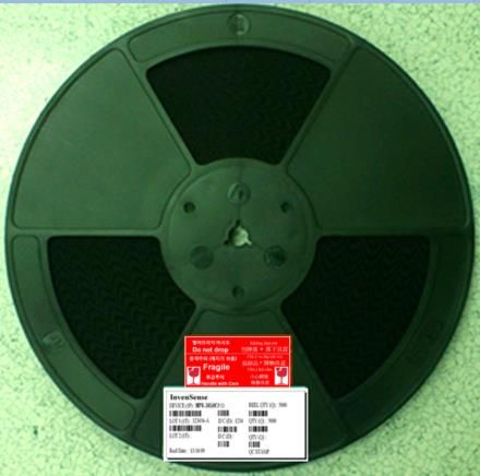
Document Number: PS-Ixx-2021A-00
                                      IDG-2021 & IXZ-2021 Product Specification                                   Revision: 2.2
                                                                                                                  Release Date: 10/17/2013

CONTENTS
1     DOCUMENT INFORMATION .....................................................................................................................4
    1.1     REVISION HISTORY .................................................................................................................................4
    1.2     PURPOSE AND SCOPE ............................................................................................................................5
    1.3     PRODUCT OVERVIEW..............................................................................................................................5
    1.4     APPLICATIONS ........................................................................................................................................5
2     FEATURES .................................................................................................................................................6
    2.1     SENSORS ...............................................................................................................................................6
    2.2     DIGITAL OUTPUT ....................................................................................................................................6
    2.3     DATA PROCESSING ................................................................................................................................6
    2.4     CLOCKING ..............................................................................................................................................6
    2.5     POWER ..................................................................................................................................................6
    2.6     PACKAGE ...............................................................................................................................................6
3     ELECTRICAL CHARACTERISTICS ..........................................................................................................7
    3.1     SENSOR SPECIFICATIONS .......................................................................................................................7
    3.2     ELECTRICAL SPECIFICATIONS..................................................................................................................8
    3.3     ELECTRICAL SPECIFICATIONS, CONTINUED ..............................................................................................9
    3.4     ELECTRICAL SPECIFICATIONS, CONTINUED ............................................................................................10
    3.5     I2C TIMING CHARACTERIZATION ............................................................................................................11
    3.6     SPI TIMING CHARACTERIZATION ...........................................................................................................12
    3.7     ABSOLUTE MAXIMUM RATINGS ..............................................................................................................13
4     APPLICATIONS INFORMATION .............................................................................................................14
    4.1     PIN OUT AND SIGNAL DESCRIPTION.......................................................................................................14
    4.2     TYPICAL OPERATING CIRCUIT ...............................................................................................................15
    4.3     BILL OF MATERIALS FOR EXTERNAL COMPONENTS.................................................................................15
5     FUNCTIONAL OVERVIEW .......................................................................................................................16
    5.1     BLOCK DIAGRAM ..................................................................................................................................16
    5.2     OVERVIEW ...........................................................................................................................................16
    5.3     TWO-AXIS MEMS GYROSCOPE WITH 16-BIT ADCS AND SIGNAL CONDITIONING .....................................16
    5.4     I2C AND SPI SERIAL COMMUNICATIONS INTERFACE ...............................................................................16
    5.5     INTERNAL CLOCK GENERATION .............................................................................................................17
    5.6     SENSOR DATA REGISTERS ...................................................................................................................17
    5.7     FIFO ...................................................................................................................................................17
    5.8     INTERRUPTS.........................................................................................................................................17
    5.9     DIGITAL-OUTPUT TEMPERATURE SENSOR .............................................................................................17
    5.10    BIAS AND LDO .....................................................................................................................................17
6     DIGITAL INTERFACE...............................................................................................................................18
    6.1     I2C SERIAL INTERFACE .........................................................................................................................18
7     SERIAL INTERFACE CONSIDERATIONS ..............................................................................................23
    7.1     SUPPORTED INTERFACES .....................................................................................................................23
    7.2     LOGIC LEVELS ......................................................................................................................................23
8     ASSEMBLY ...............................................................................................................................................24
    8.1     ORIENTATION OF AXES .........................................................................................................................24
    8.2     PACKAGE DIMENSIONS .........................................................................................................................25
    8.3     PCB DESIGN GUIDELINES.....................................................................................................................25
    8.4     PRODUCT MARKING SPECIFICATION ......................................................................................................27

Confidential & Proprietary                                               2 of 36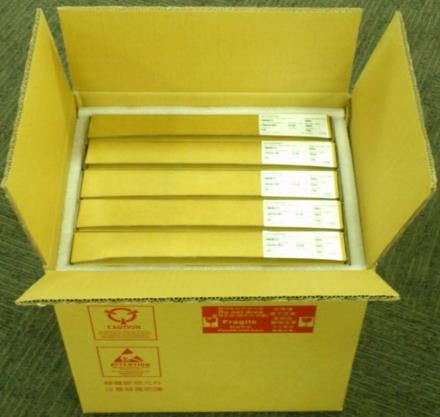
Document Number: PS-Ixx-2021A-00
                                        IDG-2021 & IXZ-2021 Product Specification                                   Revision: 2.2
                                                                                                                    Release Date: 10/17/2013

    8.5       TAPE & REAL SPECIFICATION ................................................................................................................27
    8.6       ASSEMBLY PRECAUTIONS .....................................................................................................................29
    8.7       STORAGE SPECIFICATIONS ...................................................................................................................32
    8.8       LABEL ..................................................................................................................................................32
    8.9       PACKAGING..........................................................................................................................................33
    8.10      REPRESENTATIVE SHIPPING CARTON LABEL ..........................................................................................34
9     RELIABILITY ............................................................................................................................................35
    9.1       QUALIFICATION TEST POLICY ................................................................................................................35
    9.2       QUALIFICATION TEST PLAN ...................................................................................................................35
10         ENVIRONMENTAL COMPLIANCE ......................................................................................................36

Confidential & Proprietary                                                 3 of 36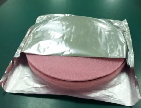
Document Number: PS-Ixx-2021A-00
                              IDG-2021 & IXZ-2021 Product Specification             Revision: 2.2
                                                                                    Release Date: 10/17/2013

1      Document Information
       1.1   Revision History

      Date       Revision                                                Description
    09/23/2011     1.0      Initial Release
    12/06/2011     1.1      Separated IXZ-2021 and IDG-2021 to a separate document.
                            Updated clock source descriptions (Section 5.5)
    03/26/2013     2.0       •    Reduced sensitivity to ¼ of previous values to get around 2 errata items noted against revision 1.x
                                  of the data sheet
                             •    Operating temperature specified as -10°C to +75°
                             •    Sensitivity and Offset operating temp changed to -10°C to +75°
                             •    Specified sensitivity over temp min/max as ±4%
                             •    Specified Sensitivity Scale Factor Tolerance min/max as ±3%
                             •    Temperature Sensor range specified as -10°C to +75°
                             •    Normal typical operating current changed to 2.9 mA (2 axes) & 3.1 mA max.
                             •    Added Gyro mechanical frequency as 27 KHz typ with 25.6 & 29 as min & max
                             •    Specified Sensor Mechanical Bandwidth Frequency at of 1.2 KHz min.
                             •    Added phase delay data for DLPF 0, 1 and 2 filter settings in Sec 3.4
                             •    Added max value for Total RMS Noise for both 92 and 184Hz DLPF settings & Low-frequency RMS
                                  noise and 1-10Hz
                             •    SART-UP TIME FOR REGISTER READ/WRITE typ changed from TBD to 20mS
                             •    Temp sensor Sensitivity, Untrimmed changed from TBD to 321.4 LSB/ºC
                             •    Temp sensor Room-Temperature Offset changed from 35 ºC /TBD to 21 ºC/0
                             •    Removed 0.9 MHz as minimum SPI speed and added 20 MHz read only mode
                             •    Changed Absolute Maximum Ratings for VDD & VDDIO to 4.0 V (was 3.6V before)
                             •    Added Product Marking Specification
                             •    Added T&R specification.
                             •    Added 256Hz LPF RMS noise.
                             •    Added P-P noise data base on RMS values for all 3 LPF settings.
                             •    Added notes to key spec on production v. validation/characterization verification
                             •    Added max Cross-Axis Sensitivity error
                             •    Added assembly precaution and reflow data
                             •    Updated the Tape & Real image with a higher resolution one
                             •    Added notes to Electrical spec to specify production tests v. validation/char data
                             •    Updated Sleep Mode Current Typ and Max values
                             •    Added Package Label section
                             •    Initial ZRO Tolerance changed from ±5 Typ to ±15 min/max per qual data
                             •    ZRO variation over temp changed from ±20 to ±5 min/max with temp comp
                             •    Absolute Max Ratings “Supply Voltage, VDD” and VDDIO changed to +4.0V
                             •    VDD & VDDIO Power-Supply Ramp Rate Min. changed to 0.1ms from 1ms
                             •    Added 0.1 to 1Hz noise specification typ and max
                             •    Added Gyro Start up time from Power On mode and clarified this as chip “ready”
                             •    Added Temp sensor linearity “max” value
                             •    In “Pin Out and Signal Description” table, clarified VDDIO as “I/O supply voltage” and VDD as
                                  “Power supply voltage”.
                             •    “SPI Timing Characterization”: Separated 1MHz & 20 MHz timing tables, added/revised timing
                                  parameters and corrected two labels on the timing chart.
                             •    Package dimension ref. “C” changed to 0.2mm (was 0.127) to be more accurate.
                             •    Changed “Specified temperature range” to “Specification Temperature Range” to indicate clearly
                                  that specifications are covered within temp range specified (unless noted otherwise).
                             •    Reduced Cross-Axis Sensitivity max value from ±6% to ±5%.
                             •    Updated JEDEC spec numbers (section 9.2)
                             •    Improved POD diagram and Revised PCB design guideline (remove extended pad requirement)
    03/28/2013     2.1       Corrected Package Dimensions Table (section 8.1)
    10/17/2013     2.2       •    Fixed typo on pk-pk noise number (DLPFCFG=0 (256 Hz)) from 3.0 to 1.2 dps

Confidential & Proprietary                             4 of 36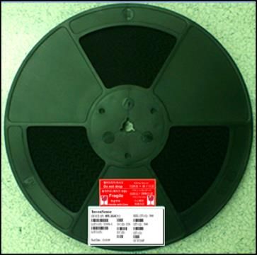
Document Number: PS-Ixx-2021A-00
                             IDG-2021 & IXZ-2021 Product Specification        Revision: 2.2
                                                                              Release Date: 10/17/2013

                           •    Changed gyro minimum mechanical frequency from 25.6 to 25 kHz

     1.2    Purpose and Scope
This document is a preliminary product specification, providing a description, specifications, and design related
information for the Digital Still Camera & Digital Video Camera Optical Image Stabilization (OIS) two axis
gyroscopes, IDG-2021™ and IXZ-2021™. Both devices are housed in small 3x3x0.75mm QFN package and
are pin and function compatible.

For references to register map and descriptions of individual registers, please refer to the IDG-2021 and IXZ-
2021 Register Map and Register Descriptions document.

     1.3    Product Overview
The IDG-2021 and IXZ-2021 are single-chip, digital output, 2 Axis MEMS gyroscope ICs which feature a 512-
byte FIFO. In applications such as Electronic Image Stabilization, the gyro output is sampled at a fast rate,
e.g.1 KHz, but is only needed at the video frame rate (ex: 30 fps). The FIFO can store the samples within a
frame, lower the traffic on the serial bus interface, and reduce power consumption by allowing the system
processor to burst read sensor data and then go into a low-power mode. The FSYNC (Frame Sync) input
allows precise timing to be achieved with Video Frame Sync at the host level for read out of the frame data.

The OIS gyros include specific features to enhance OIS performance including a narrow programmable full-
scale range of ±31.25, ±62.5, ±125, and ±250 degrees/sec, fast sampling of the gyro output at up to 32KHz,
low phase delay including fast 20MHz read out through SPI interface, very low Rate noise at 0.0065 dps/√Hz
and extremely low power consumption at 2.9 mA for 2 axis operation. Factory-calibrated initial sensitivity
reduces production-line calibration requirements.

Other industry-leading features include on-chip 16-bit ADCs, programmable digital filters, a precision clock
with 1% drift from -40°C to 85°C, an embedded temperature sensor, and programmable interrupts. The device
features I2C and SPI serial interfaces, a VDD operating range of 1.71 to 3.6V, and a separate digital IO supply,
VDDIO from 1.71V to 3.6V.

By leveraging its patented and volume-proven Nasiri-Fabrication platform, which integrates MEMS wafers with
companion CMOS electronics through wafer-level bonding, InvenSense has driven the gyro package size
down to a footprint and thickness of 3x3x0.75mm (16-pin QFN), to provide a very small yet high performance
low cost package. The device provides high robustness by supporting 10,000g shock reliability.

Sensor Axes for each device
                     Device                         IDG-2021                    IXZ-2021
                      Gyro Axes                        X, Y                       X, Z

     1.4    Applications
       •   Optical Image Stabilization for Digital Still Camera and Video Cameras
       •   Electronic Image Stabilization for video jitter compensation

Confidential & Proprietary                         5 of 36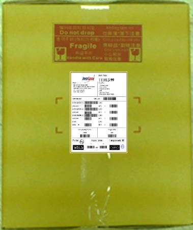
Document Number: PS-Ixx-2021A-00
                             IDG-2021 & IXZ-2021 Product Specification      Revision: 2.2
                                                                            Release Date: 10/17/2013

2   Features
The IDG-2021 and IXZ-2021 MEMS gyroscopes include a wide range of features:
     2.1   Sensors
       •   Monolithic angular rate sensor (gyros) integrated circuit
       •   Available in XY (IDG-2021) and XZ (IXZ-2021) versions.
       •   Digital-output temperature sensor
       •   External sync signal connected to the FSYNC pin supports image, video and GPS synchronization
       •   Factory calibrated scale factor
       •   High cross-axis isolation via proprietary MEMS design
       •   10,000g shock tolerant
     2.2   Digital Output
       •   Fast Mode (400kHz) I2C serial interface
       •   1 MHz SPI serial interface for full read/write capability
       •   20 MHz SPI to read gyro sensor & temp sensor data.
       •   16-bit ADCs for digitizing sensor outputs
       •   User-programmable full-scale-range of ±31.25°/sec, ±62.5°/sec, ±125°/sec and ±250°/sec
     2.3   Data Processing
       •   The total data set obtained by the device includes gyroscope data, temperature data, and the one
           bit external sync signal connected to the FSYNC pin.
       •   FIFO allows burst read, reduces serial bus traffic and saves power on the system processor.
       •   FIFO can be accessed through both I2C and SPI interfaces.
       •   Programmable interrupt
       •   Programmable low-pass filters
     2.4   Clocking
       •   On-chip timing generator clock frequency ±1% drift over full temperature range
     2.5   Power
       •   VDD supply voltage range of 1.71V to 3.6V
       •   Flexible VDDIO reference voltage allows for multiple I2C and SPI interface voltage levels
       •   Power consumption for two axes active: 2.9mA
       •   Sleep mode: 5μA
       •   Each axis can be individually powered down
     2.6   Package
       •   3x3x0.75mm footprint and maximum thickness 16-pin QFN plastic package
       •   MEMS structure hermetically sealed at wafer level
       •   RoHS and Green compliant

Confidential & Proprietary                       6 of 36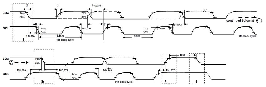
Document Number: PS-Ixx-2021A-00
                                  IDG-2021 & IXZ-2021 Product Specification        Revision: 2.2
                                                                                   Release Date: 10/17/2013

3     Electrical Characteristics
       3.1     Sensor Specifications
Typical Operating Circuit of Section 4.2, VDD = 2.5V, VDDIO = 1.8V, TA=25°C.
    Parameter                                 Conditions                     Min    Typical     Max       Unit        Notes
    GYRO SENSITIVITY
    Full-Scale Range                          FS_SEL=0                               ±31.25                º/s         1
                                              FS_SEL=1                                ±62.5                º/s
                                              FS_SEL=2                                ±125                 º/s
                                              FS_SEL=3                                ±250                 º/s

    Sensitivity Scale Factor                  FS_SEL=0                                262               LSB/(º/s)
                                              FS_SEL=1                                131               LSB/(º/s)
                                              FS_SEL=2                                65.5              LSB/(º/s)
                                              FS_SEL=3                                32.8              LSB/(º/s)
    Gyro ADC Word Length                                                               16                 bits
    Sensitivity Scale Factor Tolerance        25°C                           -3                  +3        %           1
    Sensitivity Scale Factor Variation Over   -10°C to +75°                  -4                  +4        %           2
    Temperature
    Nonlinearity                              Best fit straight line; 25°C            ±0.1                 %           2
    Cross-Axis Sensitivity                                                   -5        ±2        +5        %           1
    GYRO ZERO-RATE OUTPUT (ZRO)
    Initial ZRO Tolerance                     25°C                           -15                +15        º/s         1
    ZRO Variation Over Temperature            -10°C to +75°C                  -5                +5         º/s         2
    GYRO NOISE PERFORMANCE                    FS_SEL=0
    Total RMS Noise                           DLPFCFG=2 (92 Hz)                      0.075      0.15    º/s-r m s      1
                                              DLPFCFG=1 (184 Hz)                      0.10      0.20    º/s-r m s
                                              DLPFCFG=0 (256 Hz)                      0.12      0.23    º/s-r m s
    Total Peak-to-Peak Noise                  DLPFCFG=2 (92 Hz)                       0.37      0.75     º/s-p-p       3
                                              DLPFCFG=1 (184 Hz)                      0.50       1.0     º/s-p-p
                                              DLPFCFG=0 (256 Hz)                      0.60       1.2     º/s-p-p
    Low-frequency RMS noise                   Bandwidth 1Hz to10Hz                   0.025              º/s-r m s
                                              Bandwidth 0.1 to 1Hz                    0.01      0.03    º/s-r m s      1
    Rate Noise Spectral Density               At 10Hz                                0.0065             º/s/√Hz
    GYRO MECHANICAL
    Mechanical Frequency                                                     25       27         29       kHz          1
    Sensor Mechanical Bandwidth                                              1.2                          kHz          2
    GYRO START-UP TIME                        DLPFCFG=0, to ±1º/s of Final
    ZRO Settling                              From Sleep Mode to ready                35         50       ms
                                              From Power On to ready                  50         70       ms
    TEMPERATURE SENSOR                                                                                                 2
    Range                                     Untrimmed                            -10 to +75              ºC
    Sensitivity                                                                      321.4               LSB/ºC
    Room-Temperature Offset                   21°C                                      0                 LSB
    Linearity                                                                         ±0.2                 °C
    TEMPERATURE RANGE                                                                                                  2
    Specification Temperature Range                                          -10                +75        ºC
Notes:
   1. Tested in production
   2. Derived from validation or characterization of parts, not guaranteed in production.
   3. Peak-Peak noise data is based on measurement of RMS noise in production and at 99% normal
       distribution

Confidential & Proprietary                                    7 of 36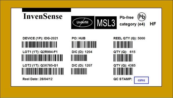
Document Number: PS-Ixx-2021A-00
                                 IDG-2021 & IXZ-2021 Product Specification             Revision: 2.2
                                                                                       Release Date: 10/17/2013

       3.2     Electrical Specifications
Typical Operating Circuit of Section 4.2, VDD = 2.5V, VDDIO = 1.8V, TA = 25°C.
    Parameters                               Conditions                      Min      Typical       Max        Units      Notes
    VDD POWER SUPPLY
    Operating Voltage Range                                                  1.71                    3.6         V         2
                                             Monotonic ramp. Ramp
    Power-Supply Ramp Rate                   rate is 10% to 90% of the        1                      100        ms         2
                                             final value
    Normal Operating Current                 Two Axes Active                            2.9          3.3        mA         1
    Sleep Mode Current                                                                   8           20         µA         1
    VDDIO REFERENCE VOLTAGE
                                                                                                                           2
    (must be regulated)
    Voltage Range                                                            1.71                    3.6         V
                                             Monotonic ramp. Ramp
    Power-Supply Ramp Rate                   rate is 10% to 90% of the        0.1                    100        ms
                                             final value
                                             10pF load, 5MHz data rate.
                                             Does not include pull up
    Normal Operating Current                                                           300                      µA
                                             resistor current draw as
                                             that is system dependent
    START-UP TIME FOR REGISTER
                                             Ready to access registers                  12           20         ms         2
    READ/WRITE
                                             AD0 = 0                                  1101000
    I2C ADDRESS
                                             AD0 = 1                                  1101001
    DIGITAL INPUTS (FSYNC, AD0,                                                                                            2
    SCLK, SDI, /CS)
    VIH, High Level Input Voltage                                         0.7*VDDIO                             V
    VIL, Low Level Input Voltage                                                                 0.3*VDDIO      V
    CI, Input Capacitance
Document Number: PS-Ixx-2021A-00
                                 IDG-2021 & IXZ-2021 Product Specification                  Revision: 2.2
                                                                                            Release Date: 10/17/2013

       3.3    Electrical Specifications, continued
Typical Operating Circuit of Section 4.2, VDD = 2.5V, VDDIO = 1.8V, TA=25°C.
  Parameters                                    Conditions                 Min   Typical                    Max     Units   Notes
   2
  I C I/O (SCL, SDA)                                                                                                           2
  VIL, LOW Level Input Voltage                                                     -0.5V to 0.3*VDDIO                V
  VIH, HIGH-Level Input Voltage                                                   0.7*VDDIO to VDDIO +               V
                                                                                          0.5V
  Vhys, Hysteresis                                                                     0.1*VDDIO                     V
  VOL1, LOW-Level Output Voltage                3mA sink current                            0 to 0.4                 V
  IOL, LOW-Level Output Current                 VOL = 0.4V                                     3                     mA
                                                VOL = 0.6V                                     6                     mA
  Output Leakage Current                                                                      100                    nA
  tof, Output Fall Time from VIHmax to VILmax   Cb bus capacitance in pf             20+0.1Cb to 250                 ns
  CI, Capacitance for Each I/O pin                                                           < 10                    pF
  INTERNAL CLOCK SOURCE                                                                                                        2
                                                Fchoice=0,1,2
                                                                                              32                    kHz
                                                SMPLRT_DIV=0
                                                Fchoice=3;
  Sample Rate                                   DLPFCFG=0 or 7                                 8                    kHz
                                                SMPLRT_DIV=0
                                                Fchoice=3;
                                                DLPFCFG=1,2,3,4,5,6;                           1                    kHz
                                                SMPLRT_DIV=0
  Clock Frequency Initial Tolerance             CLK_SEL=0, 6; 25°C         -2                                +2      %
                                                CLK_SEL=1,2,3,4,5; 25°C    -1                                +1      %
  Frequency Variation over Temperature          CLK_SEL=0,6                                -10 to +10                %
                                                CLK_SEL=1,2,3,4,5                             ±1                     %
  PLL Settling Time                             CLK_SEL=1,2,3,4,5                              4                     ms
Notes:
   1. Tested in production
   2. Derived from validation or characterization of parts, not guaranteed in production.

Confidential & Proprietary                                    9 of 36
Document Number: PS-Ixx-2021A-00
IDG-2021 & IXZ-2021 Product Specification Revision: 2.2
Release Date: 10/17/2013
3.4 Electrical Specifications, continued
Typical Operating Circuit of Section 4.2, VDD = 2.5V, VDDIO = 1.8V, TA=25°C.
DLPF
Parameters Fchoice Bandwidth Frequency Phase Delay Units
Configuration
Phase Delay 1 0
With SPI @ 20MHz
1 0 X Bypass 20Hz 0.9 Deg
0 0 0 250Hz 20Hz 7 Deg
10Hz 3.5 Deg
0 0 1 184Hz 20Hz 20 Deg
10Hz 10 Deg
0 0 2 92Hz 20Hz 28 Deg
, 10Hz 14 Deg
Confidential & Proprietary 10 of 36Document Number: PS-Ixx-2021A-00
IDG-2021 & IXZ-2021 Product Specification Revision: 2.2
Release Date: 10/17/2013
3.5 I2C Timing Characterization
Typical Operating Circuit of Section 4.2, VDD = 2.5V, VDDIO = 1.8V, TA=25°C.
Parameters Conditions Min Typical Max Units Notes
I2 C TIMING I2 C FAST-MODE 2
fSCL, SCL Clock Frequency 0 400 kHz
tHD.STA, (Repeated) START Condition 0.6 µs
Hold Time
tLOW, SCL Low Period 1.3 µs
tHIGH, SCL High Period 0.6 µs
tSU.STA, Repeated START Condition 0.6 µs
Setup Time
tHD.DAT, SDA Data Hold Time 0 µs
tSU.DAT, SDA Data Setup Time 100 ns
tr, SDA and SCL Rise Time Cb bus cap. from 10 to 20+0.1 300 ns
400pF Cb
tf, SDA and SCL Fall Time Cb bus cap. from 10 to 20+0.1 300 ns
400pF Cb
tSU.STO, STOP Condition Setup Time 0.6 µs
tBUF, Bus Free Time Between STOP and 1.3 µs
START Condition
Cb, Capacitive Load for each Bus Line < 400 pF
tVD.DAT, Data Valid Time 0.9 µs
tVD.ACK, Data Valid Acknowledge Time 0.9 µs
Notes:
1. Tested in production
2. Derived from validation or characterization of parts, not guaranteed in production.
I2C Bus Timing Diagram
Confidential & Proprietary 11 of 36Document Number: PS-Ixx-2021A-00
IDG-2021 & IXZ-2021 Product Specification Revision: 2.2
Release Date: 10/17/2013
3.6 SPI Timing Characterization
Typical Operating Circuit of Section 4.2, VDD = 2.5V, VDDIO = 1.8V, TA = 25°C.
Parameters Conditions Min Typical Max Units Notes
SPI TIMING (fSCLK = 1 MHz) R/W 2
fSCLK, SCLK Clock Frequency 1 MHz
tLOW, SCLK Low Period 400 ns
tHIGH, SCLK High Period 400 ns
tSU.CS, CS Setup Time 8 ns
tHD.CS, CS Hold Time 500 ns
tSU.SDI, SDI Setup Time 11 ns
tHD.SDI, SDI Hold Time 7 ns
tVD.SDO, SDO Valid Time Cload = 20pF 100 ns
tHD.SDO, SDO Hold Time 4
tDIS.SDO, SDO Output Disable Time 50 ns
tBUF, CS high time between transactions 600 ns
Parameters Conditions Min Typical Max Units Notes
3
SPI TIMING (fSCLK = 20 MHz) Read 2
fSCLK, SCLK Clock Frequency 20 MHz
tLOW, SCLK Low Period - 25 - ns
tHIGH, SCLK High Period - 25 - ns
tSU.CS, CS Setup Time 25 ns
tHD.CS, CS Hold Time 25 ns
tSU.SDI, SDI Setup Time 5 ns
tHD.SDI, SDI Hold Time 6 ns
tVD.SDO, SDO Valid Time Cload = 20pF 30 ns
tHD.SDO, SDO Hold Time 4
tDIS.SDO, SDO Output Disable Time 25 ns
tBUF, CS high time between transactions 600 ns
Notes:
1. Tested in production
2. Derived from validation or characterization of parts, not guaranteed in production.
3. Read of Sensor registers only
/CS
SCLK
SDI
SDO
SPI Bus Timing Diagram
Confidential & Proprietary 12 of 36Document Number: PS-Ixx-2021A-00
IDG-2021 & IXZ-2021 Product Specification Revision: 2.2
Release Date: 10/17/2013
3.7 Absolute Maximum Ratings
Stress above those listed as “Absolute Maximum Ratings” may cause permanent damage to the device. These
are stress ratings only and functional operation of the device at these conditions is not implied. Exposure to
the absolute maximum ratings conditions for extended periods may affect device reliability.
Absolute Maximum Ratings
Parameter Rating
Supply Voltage, VDD -0.5V to 4.0V
VDDIO Input Voltage Level -0.5V to 4.0V
REGOUT -0.5V to 2V
Input Voltage Level (AD0, FSYNC) -0.5V to VDDIO
SCL, SDA, INT (SPI enable) -0.5V to VDDIO
SCL, SDA, INT (SPI disable) -0.5V to VDDIO
Acceleration (Any Axis, unpowered) 10,000g for 0.2ms
Operating Temperature Range -40°C to +85°C
Storage Temperature Range -40°C to +125°C
Electrostatic Discharge (ESD) Protection 2kV (HBM); 250V (MM)
Latch-up JEDEC Class II (2),125°C, ±100mA
Confidential & Proprietary 13 of 36Document Number: PS-Ixx-2021A-00
IDG-2021 & IXZ-2021 Product Specification Revision: 2.2
Release Date: 10/17/2013
4 Applications Information
4.1 Pin Out and Signal Description
Pin Number
Pin Name Pin Description
3x3x0.75mm
1 SDA/SDI I2C serial data (SDA); SPI serial data input (SDI)
3 VDDIO I/O supply voltage.
4 /CS SPI chip select (0=SPI mode, 1= I2C mode)
5 RESV Reserved. Do not connect.
6 AD0 / SDO I2C Slave Address LSB (AD0); SPI serial data output (SDO)
7 REGOUT Regulator filter capacitor connection
8 FSYNC Frame synchronization digital input. Connect to GND if not used.
9 VDD Power supply voltage
10 INT Interrupt digital output (totem pole or open-drain)
12 GND Power supply ground
14 RESV-G Reserved. Connect to Ground.
16 SCL/SCLK I2C serial clock (SCL); SPI serial clock (SCLK)
2, 11, 13, 15 NC Not internally connected. May be used for PCB trace routing.
SCL/SCLK
RESV-G
NC
NC
16 15 14 13
SDA/SDI 1 IDG-2021 12 GND +Z
NC 2 IXZ-2021 11 NC
IDG IXZ
VDDIO 3 (16-pin QFN) 10 INT - 20 -2 02
21 1
/CS 4 9 VDD
5 6 7 8 +Y +X +X
RESV
AD0/SDO
REGOUT
FSYNC
QFN Package (Top View)
16-pin, 3mm x 3mm x 0.75mm Orientation of Axes of Sensitivity and Polarity of Rotation
Footprint and maximum thickness
Confidential & Proprietary 14 of 36Document Number: PS-Ixx-2021A-00
IDG-2021 & IXZ-2021 Product Specification Revision: 2.2
Release Date: 10/17/2013
4.2 Typical Operating Circuit
SCL/SCLK
16 15 14 13
SDA/SDI 1 IDG-2021 12
VDDIO 2 IXZ-2021 11 GND
VDD
3 (16-pin QFN) 10 INT
C3 4 9
10nF
C2
GND 0.1µF
5 6 7 8
/CS GND
C1
0.1µF
FSYNC
AD0/SDO
GND
Typical Operating Circuit
4.3 Bill of Materials for External Components
Component Label Specification Quantity
Regulator Filter Capacitor C1 Ceramic, X7R, 0.1µF ±10%, 2V 1
VDD Bypass Capacitor C2 Ceramic, X7R, 0.1µF ±10%, 4V 1
VDDIO Bypass Capacitor C3 Ceramic, X7R, 10nF ±10%, 4V 1
Confidential & Proprietary 15 of 36Document Number: PS-Ixx-2021A-00
IDG-2021 & IXZ-2021 Product Specification Revision: 2.2
Release Date: 10/17/2013
5 Functional Overview
5.1 Block Diagram
VDD
CLOCK Factory OTP Factory
VDDIO POR
Gen Test Modes Calibration
REGOUT CSN
IIC SLAVE
AD0 / SDO
Drive block Sensing Block
GND SPI SLAVE SCL / SCLK
SDA / SDI
CV ADC Digital Low Pass Filter
Single FIFO
SENSOR
GYRO
Drive OUTPUT DRDY
CV ADC Digital Low Pass Filter
REGS
INT
INTC
FSYNC
Temp
ADC Digital Low Pass Filter
Sensor
Status
Automatic Gain Registers
Control
Charge Reference Voltage Control
Self test Trims and config ckts
Pump Gen Regulator Registers
5.2 Overview
Both the IDG-2021 and IXZ-2021 are comprised of the following key blocks / functions:
• Two-axis MEMS rate gyroscope sensors with 16-bit ADCs and signal conditioning
• Available in two axis XY and XZ configurations
• I2C and SPI serial communications interfaces
• Clocking
• Sensor Data Registers
• FIFO
• Interrupts
• Digital-Output Temperature Sensor
• Bias and LDO
5.3 Two-Axis MEMS Gyroscope with 16-bit ADCs and Signal Conditioning
Both the IDG-2021 and IXZ-2021 consist of a single structure vibratory MEMS rate gyroscope, which detects
rotation about the X&Y or X&Z axes, respectively. When the gyro is rotated about any of the sense axes, the
Coriolis Effect causes a vibration that is detected by a capacitive pick off. The resulting signal is amplified,
demodulated, and filtered to produce a voltage that is proportional to the angular rate. This voltage is digitized
using individual on-chip 16-bit Analog-to-Digital Converters (ADCs) to sample each axis. The chip features a
programmable full-scale range of the gyro sensors of ±31.25, ±62.5, ±125, and ±250 dps. The FSR range is
optimized for image stabilization applications where the narrower range improves hand jitter detection accuracy
via the 16 bit ADCs. User-selectable low-pass filters enable a wide range of cut-off frequencies. The ADC
sample rate can be programmed to 32 kHz, 8 kHz, 1 kHz, 500 Hz, 333.3 Hz, 250 Hz, 200 Hz, 166.7 Hz, 142.9
Hz, or 125 Hz.
5.4 I2C and SPI Serial Communications Interface
The IDG-2021 and IXZ-2021 have both I2C and SPI serial interfaces. The device always acts as a slave when
communicating to the system processor. The logic level for communications to the master is set by the voltage
Confidential & Proprietary 16 of 36Document Number: PS-Ixx-2021A-00
IDG-2021 & IXZ-2021 Product Specification Revision: 2.2
Release Date: 10/17/2013
on the VDDIO pin. The LSB of the of the I2C slave address is set by the AD0 pin. The I2C and SPI protocols
are described in more detail in Section 6.
5.5 Internal Clock Generation
Both the IDG-2021 and IXZ-2021 use a flexible clocking scheme, allowing for a variety of internal clock sources
for the internal synchronous circuitry. This synchronous circuitry includes the signal conditioning and ADCs,
various control circuits, and registers.
Allowable internal sources for generating the internal clock are:
• An internal relaxation oscillator
• PLL (gyroscope based clock)
In order for the gyroscope to perform to spec, the PLL must be selected as the clock source. When the internal
20MHz oscillator is chosen as the clock source, the device can operate while having the gyroscopes disabled.
However, this is only recommended if the user wishes to use the internal temperature sensor in this mode.
5.6 Sensor Data Registers
The sensor data registers contain the latest gyro and temperature data. They are read-only registers, and are
accessed via the Serial Interface. Data from these registers may be read anytime, however, the interrupt
function may be used to determine when new data is available.
5.7 FIFO
Both the IDG-2021 and IXZ-2021 contain a 512-byte FIFO register that is accessible via the both the I2C and
SPI Serial Interfaces. The FIFO configuration register determines what data goes into it, with possible choices
being gyro data, temperature readings and FSYNC input. A FIFO counter keeps track of how many bytes of
valid data are contained in the FIFO. The FIFO register supports burst reads. The interrupt function may be
used to determine when new data is available.
5.8 Interrupts
Interrupt functionality is configured via the Interrupt Configuration register. Items that are configurable include
the INT pin configuration, the interrupt latching and clearing method, and triggers for the interrupt. Items that
can trigger an interrupt are (1) Clock generator locked to new reference oscillator (used when switching clock
sources), (2) new data is available to be read (from the FIFO and Data registers), and (3) FIFO overflow. The
interrupt status can be read from the Interrupt Status register.
5.9 Digital-Output Temperature Sensor
An on-chip temperature sensor and ADC are used to measure the device’s die temperature. The readings
from the ADC can be read from the FIFO or the Sensor Data registers.
5.10 Bias and LDO
The bias and LDO section generates the internal supply and the reference voltages and currents required by
the IDG-2021 and IXZ-2021. Its two inputs are unregulated VDD of 1.71V to 3.6V and a VDDIO logic reference
supply voltage of 1.71V to 3.6V. The LDO output is bypassed by a 0.1µF capacitor at REGOUT.
Confidential & Proprietary 17 of 36Document Number: PS-Ixx-2021A-00
IDG-2021 & IXZ-2021 Product Specification Revision: 2.2
Release Date: 10/17/2013
6 Digital Interface
6.1 I2C Serial Interface
The internal registers and memory of the IDG-2021 and IXZ-2021 can be accessed using the I2C interface.
Serial Interface
Pin Number Pin Name Pin Description
3 VDDIO Digital I/O supply voltage.
6 AD0 / SDO I2C Slave Address LSB (AD0); SPI serial data output (SDO)
16 SCL / SCLK I2C serial clock (SCL); SPI serial clock (SCLK)
1 SDA / SDI I2C serial data (SDA); SPI serial data input (SDI)
6.1.1 I2C Interface
I2C is a two-wire interface comprised of the signals serial data (SDA) and serial clock (SCL). In general, the
lines are open-drain and bi-directional. In a generalized I2C interface implementation, attached devices can be
a master or a slave. The master device puts the slave address on the bus, and the slave device with the
matching address acknowledges the master.
Both the IDG-2021 and IXZ-2021 always operate as a slave device when communicating to the system
processor, which thus acts as the master. SDA and SCL lines typically need pull-up resistors to VDD. The
maximum bus speed is 400 kHz.
The slave address of the device is b110100X which is 7 bits long. The LSB bit of the 7 bit address is determined
by the logic level on pin AD0. This allows two IDG-2021 or IXZ-2021 devices to be connected to the same I2C
bus. When used in this configuration, the address of the one of the devices should be b1101000 (pin AD0 is
logic low) and the address of the other should be b1101001 (pin AD0 is logic high). The I 2C address is stored
in WHO_AM_I register.
I2C Communications Protocol
START (S) and STOP (P) Conditions
Communication on the I2C bus starts when the master puts the START condition (S) on the bus, which is
defined as a HIGH-to-LOW transition of the SDA line while SCL line is HIGH (see figure below). The bus is
considered to be busy until the master puts a STOP condition (P) on the bus, which is defined as a LOW to
HIGH transition on the SDA line while SCL is HIGH (see figure below).
Additionally, the bus remains busy if a repeated START (Sr) is generated instead of a STOP condition.
SDA
SCL
S P
START condition STOP condition
START and STOP Conditions
Confidential & Proprietary 18 of 36Document Number: PS-Ixx-2021A-00
IDG-2021 & IXZ-2021 Product Specification Revision: 2.2
Release Date: 10/17/2013
Data Format / Acknowledge
I2C data bytes are defined to be 8 bits long. There is no restriction to the number of bytes transmitted per data
transfer. Each byte transferred must be followed by an acknowledge (ACK) signal. The clock for the
acknowledge signal is generated by the master, while the receiver generates the actual acknowledge signal
by pulling down SDA and holding it low during the HIGH portion of the acknowledge clock pulse.
If a slave is busy and is unable to transmit or receive another byte of data until some other task has been
performed, it can hold SCL LOW, thus forcing the master into a wait state. Normal data transfer resumes when
the slave is ready, and releases the clock line (refer to the following figure).
DATA OUTPUT BY
TRANSMITTER (SDA)
not acknowledge
DATA OUTPUT BY
RECEIVER (SDA)
acknowledge
SCL FROM
1 2 8 9
MASTER
clock pulse for
START acknowledgement
condition
Acknowledge on the I2C Bus
Communications
After beginning communications with the START condition (S), the master sends a 7-bit slave address followed
by an 8th bit, the read/write bit. The read/write bit indicates whether the master is receiving data from or is
writing to the slave device. Then, the master releases the SDA line and waits for the acknowledge signal (ACK)
from the slave device. Each byte transferred must be followed by an acknowledge bit. To acknowledge, the
slave device pulls the SDA line LOW and keeps it LOW for the high period of the SCL line. Data transmission
is always terminated by the master with a STOP condition (P), thus freeing the communications line. However,
the master can generate a repeated START condition (Sr), and address another slave without first generating
a STOP condition (P). A LOW to HIGH transition on the SDA line while SCL is HIGH defines the stop condition.
All SDA changes should take place when SCL is low, with the exception of start and stop conditions.
SDA
SCL 1–7 8 9 1–7 8 9 1–7 8 9
S P
START ADDRESS R/W ACK DATA ACK DATA ACK STOP
condition condition
Complete I2C Data Transfer
Confidential & Proprietary 19 of 36Document Number: PS-Ixx-2021A-00
IDG-2021 & IXZ-2021 Product Specification Revision: 2.2
Release Date: 10/17/2013
To write the internal IDG-2021 or IXZ-2021 registers, the master transmits the start condition (S), followed by
the I2C address and the write bit (0). At the 9th clock cycle (when the clock is high), the device acknowledges
the transfer. Then the master puts the register address (RA) on the bus. After the device acknowledges the
reception of the register address, the master puts the register data onto the bus. This is followed by the ACK
signal, and data transfer may be concluded by the stop condition (P). To write multiple bytes after the last ACK
signal, the master can continue outputting data rather than transmitting a stop signal. In this case, the device
automatically increments the register address and loads the data to the appropriate register. The following
figures show single and two-byte write sequences.
Single-Byte Write Sequence
Master S AD+W RA DATA P
Slave ACK ACK ACK
Burst Write Sequence
Master S AD+W RA DATA DATA P
Slave ACK ACK ACK ACK
To read the internal device registers, the master sends a start condition, followed by the I2C address and a
write bit, and then the register address that is going to be read. Upon receiving the ACK signal from the device,
the master transmits a start signal followed by the slave address and read bit. As a result, the device sends an
ACK signal and the data. The communication ends with a not acknowledge (NACK) signal and a stop bit from
master. The NACK condition is defined such that the SDA line remains high at the 9 th clock cycle. The following
figures show single and two-byte read sequences.
Single-Byte Read Sequence
Master S AD+W RA S AD+R NACK P
Slave ACK ACK ACK DATA
Burst Read Sequence
Master S AD+W RA S AD+R ACK NACK P
Slave ACK ACK ACK DATA DATA
Confidential & Proprietary 20 of 36Document Number: PS-Ixx-2021A-00
IDG-2021 & IXZ-2021 Product Specification Revision: 2.2
Release Date: 10/17/2013
I2C Terms
Signal Description
S Start Condition: SDA goes from high to low while SCL is high
AD Slave I2C address
W Write bit (0)
R Read bit (1)
ACK Acknowledge: SDA line is low while the SCL line is high at the 9th clock cycle
NACK Not-Acknowledge: SDA line stays high at the 9th clock cycle
RA The internal register address
DATA Transmit or received data
P Stop condition: SDA going from low to high while SCL is high
6.1.2
6.1.3 SPI interface
SPI is a 4-wire synchronous serial interface that uses two control and two data lines. Both the IDG-2021 and
IXZ-2021 always operate as a Slave device during standard Master-Slave SPI operation. With respect to the
Master, the Serial Clock output (SCLK), the Data Output (SDO) and the Data Input (SDI) are shared among
the Slave devices. The Master generates an independent Chip Select (/CS) for each Slave device; /CS goes
low at the start of transmission and goes back high at the end. The Serial Data Output (SDO) line, remains in
a high-impedance (high-z) state when the device is not selected, so it does not interfere with any active devices.
SPI Operational Features
1. Data is delivered MSB first and LSB last
2. Data is latched on rising edge of SCLK
3. Data should be transitioned on the falling edge of SCLK
4. SCLK frequency is 1MHz max for SPI in full read/write capability mode. When the SPI frequency
is set to 20MHz, its operation is limited to reading sensor registers only.
5. SPI read and write operations are completed in 16 or more clock cycles (two or more bytes). The
first byte contains the SPI Address, and the following byte(s) contain(s) the SPI data. The first bit
of the first byte contains the Read/Write bit and indicates the Read (1) or Write (0) operation. The
following 7 bits contain the Register Address. In cases of multiple-byte Read/Writes, data is two
or more bytes:
SPI Address format
MSB LSB
R/W A6 A5 A4 A3 A2 A1 A0
SPI Data format
MSB LSB
D7 D6 D5 D4 D3 D2 D1 D0
6. Supports Single or Burst Read/Writes.
Confidential & Proprietary 21 of 36Document Number: PS-Ixx-2021A-00
IDG-2021 & IXZ-2021 Product Specification Revision: 2.2
Release Date: 10/17/2013
SCLK
SDI
SPI Master SDO SPI Slave 1
/CS1 /CS
/CS2
SCLK
SDI
SDO
SPI Slave 2
/CS
Typical SPI Master / Slave Configuration
Each SPI slave requires its own Chip Select (/CS) line. SDO, SDI and SCLK lines are shared. Only one /CS
line is active (low) at a time ensuring that only one slave is selected at a time. The /CS lines of other slaves
are held high which causes their respective SDO pins to be high-Z.
Confidential & Proprietary 22 of 36Document Number: PS-Ixx-2021A-00
IDG-2021 & IXZ-2021 Product Specification Revision: 2.2
Release Date: 10/17/2013
7 Serial Interface Considerations
7.1 Supported Interfaces
Both the IDG-2021 and IXZ-2021 support I2C and SPI communication.
7.2 Logic Levels
The I/O logic levels are set to VDDIO. VDDIO may be set to be equal to VDD or to another voltage, such that
it is between 1.71 V and 3.6V at all times. Both I2C and SPI communication support VDDIO.
(0V - VDDIO) SYSTEM BUS
VDD
VDD
VDDIO VDDIO
IDG-2021
IXZ-2021 (0V - VDDIO)
INT
(0V - VDDIO) System
FSYNC Processor
(0V - VDDIO)
SDA/SDI SDA
VDDIO (0V - VDDIO)
SCL/SCLK SCL
(0V, VDDIO)
VDDIO AD0/SDO AD0/SDO
(0V, VDDIO)
/CS /CS
Confidential & Proprietary 23 of 36Document Number: PS-Ixx-2021A-00
IDG-2021 & IXZ-2021 Product Specification Revision: 2.2
Release Date: 10/17/2013
8 Assembly
This section provides general guidelines for assembling InvenSense Micro Electro-Mechanical Systems
(MEMS) gyros packaged in Quad Flat No leads package (QFN) surface mount integrated circuits.
8.1 Orientation of Axes
The diagram below shows the orientation of the axes of sensitivity and the polarity of rotation. Note the pin 1
identifier in the figure.
+Z
IDG IXZ
- 20 - 20
21 21
+Y +X +X
Orientation of Axes of Sensitivity and Polarity of Rotation
Confidential & Proprietary 24 of 36Document Number: PS-Ixx-2021A-00
IDG-2021 & IXZ-2021 Product Specification Revision: 2.2
Release Date: 10/17/2013
8.2 Package Dimensions
Dimensions in Millimeters
Dimension Min Nom Max
A 0.70 0.75 0.80
A1 0.00 0.02 0.05
b 0.18 0.25 0.30
c --- 0.15 ref ---
D 2.90 3.00 3.10
D2 1.65 1.70 1.75
E 2.90 3.00 3.10
E2 1.45 1.50 1.55
e --- 0.50 ---
L 0.35 0.40 0.45
L1 0.45 0.50 0.55
y 0.000 --- 0.075
8.3 PCB Design Guidelines
Do not solder the center Exposed Pad (E-pad). This is a solder keep-out area.
Recommendations:
Size the PCB pad layout to match the QFN pad leads. Use the package dimensions shown in the Table above.
The Dimensions Table is supplemented with the first figure that follows.
Confidential & Proprietary 25 of 36Document Number: PS-Ixx-2021A-00
IDG-2021 & IXZ-2021 Product Specification Revision: 2.2
Release Date: 10/17/2013
Design the PCB pad layout with Non Solder Mask Defined pads (NSDM). NSMD pads are recommended over
Solder Mask Defined (SMD) pads. NSMD pads provide a tighter tolerance on copper etching, provide a larger
copper pad area, and allow the solder to anchor to the edges of the copper pads to improve solder joint
reliability. As a recommendation, set the solder mask aperture a minimum of 0.05 mm larger than the
component solder pad per edge. Two alternative PCB layouts are shown below for reference.
Blocked Areas – Solder Mask Individually Outlined Pads – Solder Mask
D
E
Confidential & Proprietary 26 of 36Document Number: PS-Ixx-2021A-00
IDG-2021 & IXZ-2021 Product Specification Revision: 2.2
Release Date: 10/17/2013
8.4 Product Marking Specification
Part number Identification:
Product Top Mark
IDG-2021 IY21
IXZ-2021 IZ21
8.5 Tape & Real Specification
Confidential & Proprietary 27 of 36Document Number: PS-Ixx-2021A-00
IDG-2021 & IXZ-2021 Product Specification Revision: 2.2
Release Date: 10/17/2013
Package Orientation User Direction
of Feed
Pin 1
INVENSENSE INVENSENSE
Cover Tape
(Anti-Static)
Carrier Tape
(Anti-Static)
Reel HF
Terminal Tape
ee )
-f r y (
e4
Pb or
0
te g ) : 500
ca Y (Q
QT
EL
RE
0
) : 300
Y (Q
e QT
en s UB 0
en S
:H ) : 200
PO Q
Y(
Inv MP
U -60
50
(D ):
111
8 QT
AM
P:
1P
): D /C ST
E( 7 QC
VIC -F 1
DE : 110
2 R 784 (D )
): Q D /C
(1 T
T1 -G 1
LO
V 215
Q3
(1 T ):
T2
LO /11
/ 05
: 18
a te
el D
Re
Label
Tape and Reel Specification
Reel Specifications
Quantity Per Reel 5,000
Reels per Pizza Box 1
Pizza Boxes Per Carton (max) 5
Pcs/Carton (max) 25,000
Note: empty pizza boxes are included to ensure that pizza boxes don’t shift.
Confidential & Proprietary 28 of 36Document Number: PS-Ixx-2021A-00
IDG-2021 & IXZ-2021 Product Specification Revision: 2.2
Release Date: 10/17/2013
8.6 Assembly Precautions
8.6.1 Gyroscope Surface Mount Guidelines
InvenSense MEMS Gyros sense rate of rotation. In addition, gyroscopes sense mechanical stress coming from
the printed circuit board (PCB). This PCB stress can be minimized by adhering to certain design rules:
When using MEMS gyroscope components in plastic packages, PCB mounting and assembly can cause
package stress. This package stress in turn can affect the output offset and its value over a wide range of
temperatures. This stress is caused by the mismatch between the Coefficient of Linear Thermal Expansion
(CTE) of the package material and the PCB. Care must be taken to avoid package stress due to mounting.
Traces connected to pads should be as symmetric as possible. Maximizing symmetry and balance for pad
connection will help component self alignment and will lead to better control of solder paste reduction after
reflow.
Any material used in the surface mount assembly process of the MEMS gyroscope should be free of restricted
RoHS elements or compounds. Pb-free solders should be used for assembly.
8.6.2 Exposed Die Pad Precautions
The IDG-2021 and IXZ-2021 have very low active and standby current consumption. There is no electrical
connection between the exposed die pad and the internal CMOS circuits. The exposed die pad is not required
for heat-sinking, and should not be soldered to the PCB. Underfill is also not recommended. Soldering or
adding underfill to the e-pad can induce performance changes due to package thermo-mechanical stress.
8.6.3 Trace Routing
Routing traces or vias under the gyro package such that they run under the exposed die pad is prohibited.
Routed active signals may harmonically couple with the gyro MEMS devices, compromising gyro response.
The gyro drive frequency is ~27 KHz. To avoid harmonic coupling don’t route active signals in non-shielded
signal planes directly below, or above the gyro package. Note: For best performance, design a ground plane
under the e-pad to reduce PCB signal noise from the board on which the gyro device is mounted. If the gyro
device is stacked under another PCB board, design a ground plane directly above the gyro device to shield
active signals from the PCB board mounted above.
8.6.4 Component Placement
Do not place large insertion components such as keyboard or similar buttons, connectors, or shielding boxes
at a distance of less than 6 mm from the MEMS gyro. Maintain generally accepted industry design practices
for component placement near the IDG-2021 or IXZ-2021 to prevent noise coupling and thermo-mechanical
stress.
8.6.5 PCB Mounting and Cross-Axis Sensitivity
Orientation errors of the gyroscope as mounted to the printed circuit board can cause cross-axis sensitivity in
which one gyro sense axis responds to rotation or acceleration about an orthogonal axis. For example, the X-
gyro sense axis may respond to rotation about the Y or Z axes. The orientation mounting errors are illustrated
in the figure on the next page (dependent on XY or XZ configurations)
Confidential & Proprietary 29 of 36Document Number: PS-Ixx-2021A-00
IDG-2021 & IXZ-2021 Product Specification Revision: 2.2
Release Date: 10/17/2013
Z
Φ
Y
IDG
IXZ 202
- 20 1
21
Θ X
Package Gyro & Accel Axes ( ) Relative to PCB Axes ( ) with Orientation Errors (Θ and Φ)
The table below shows the cross-axis sensitivity as a percentage of the gyroscope or accelerometer’s
sensitivity for a given orientation error, respectively.
Cross-Axis Sensitivity vs. Orientation Error
Orientation Error Cross-Axis Sensitivity
(θ or Φ) (sinθ or sinΦ)
0º 0%
0.5º 0.87%
1º 1.75%
The specifications for cross-axis sensitivity in Section 6.1 and Section 6.2 include the effect of the die
orientation error with respect to the package.
8.6.6 MEMS Handling Instructions
MEMS (Micro Electro-Mechanical Systems) are a time-proven, robust technology used in hundreds of millions
of consumer, automotive and industrial products. MEMS devices consist of microscopic moving mechanical
structures. They differ from conventional IC products, even though they can be found in similar packages.
Therefore, MEMS devices require different handling precautions than conventional ICs prior to mounting onto
printed circuit boards (PCBs).
The IDG-2021 and IXZ-2021 have been qualified to a shock tolerance of 10,000g. InvenSense packages its
gyroscopes as it deems proper for protection against normal handling and shipping. It recommends the
following handling precautions to prevent potential damage.
• Do not drop individually packaged gyroscopes, or trays of gyroscopes onto hard surfaces. Components
placed in trays could be subject to g-forces in excess of 10,000g if dropped.
• Printed circuit boards that incorporate mounted gyroscopes should not be separated by manually snapping
apart. This could also create g-forces in excess of 10,000g.
• Do not clean MEMS gyroscopes in ultrasonic baths. Ultrasonic baths can induce MEMS damage if the
bath energy causes excessive drive motion through resonant frequency coupling.
8.6.7 ESD Considerations
Establish and use ESD-safe handling precautions when unpacking and handling ESD-sensitive devices.
• Store ESD sensitive devices in ESD safe containers until ready for use, such as the original moisture
sealed bags, until ready for assembly.
• Restrict all device handling to ESD protected work areas that measure less than 200V static charge.
Ensure that all workstations and personnel are properly grounded to prevent ESD.
Confidential & Proprietary 30 of 36Document Number: PS-Ixx-2021A-00
IDG-2021 & IXZ-2021 Product Specification Revision: 2.2
Release Date: 10/17/2013
8.6.8 Reflow Specification
Qualification Reflow Profile: The IDG-2021 and IXZ-2021A were qualified in accordance with IPC/JEDEC J-
STD-020D.1. This standard classifies proper packaging, storage and handling in order to avoid subsequent
thermal and mechanical damage during the solder reflow attachment phase of PCB assembly.
The qualification preconditioning process specifies a sequence consisting of a bake cycle, a moisture soak
cycle (in a temperature humidity oven), and three consecutive solder reflow cycles, followed by functional
device testing.
The peak solder reflow classification temperature requirement for package qualification is (260 +5/-0°C) for
lead-free soldering of components measuring less than 1.6 mm in thickness. The qualification profile and a
table explaining the set-points are shown below:
SOLDER REFLOW PROFILE FOR QUALIFICATION
LEAD-FREE IR/CONVECTION
F
TPmax
E G
TPmin
D 10-30sec H
TLiquidus
Tsmax C
Liquidus
Temperature [°C]
60-120sec
B Tramp-up
( < 3 C/sec) I
Tsmin Tramp-down
( < 4 C/sec)
Preheat
60-120sec
Troom-Pmax
A (< 480sec)
Time [Seconds]
Temperature Set Points Corresponding to Reflow Profile Above
CONSTRAINTS
Step Setting
Temp (°C) Time (sec) Max. Rate (°C/sec)
A Troom 25
B TSmin 150
C TSmax 200 60 < tBC < 120
D TLiquidus 217 r(TLiquidus-TPmax) < 3
E TPmin [255°C, 260°C] 255 r(TLiquidus-TPmax) < 3
F TPmax [ 260°C, 265°C] 260 tAF < 480 r(TLiquidus-TPmax) < 3
G TPmin [255°C, 260°C] 255 10< tEG < 30 r(TPmax-TLiquidus) < 4
H TLiquidus 217 60 < tDH < 120
I Troom 25
Notes: Customers must never exceed the Classification temperature (TPmax = 260°C).
All temperatures refer to the topside of the QFN package, as measured on the package body surface.
Production Reflow: Check the recommendations of your solder manufacturer. For optimum results, use lead-
free solders that have lower specified temperature profiles (Tpmax ~ 235°C). Also use lower ramp-up and ramp-
down rates than those used in the qualification profile. Never exceed the maximum conditions that we used
for qualification, as these represent the maximum tolerable ratings for the device.
Confidential & Proprietary 31 of 36Document Number: PS-Ixx-2021A-00
IDG-2021 & IXZ-2021 Product Specification Revision: 2.2
Release Date: 10/17/2013
8.7 Storage Specifications
The storage specification of the IDG-2021 and IXZ-2021 conforms to IPC/JEDEC J-STD-020D.1 Moisture
Sensitivity Level (MSL) 3.
Calculated shelf-life in moisture-sealed bag 12 months -- Storage conditions:Document Number: PS-Ixx-2021A-00
IDG-2021 & IXZ-2021 Product Specification Revision: 2.2
Release Date: 10/17/2013
8.9 Packaging
To improve protection for QFN contained in the reel, the reel is packed directly in 10mm thick ESD foam inside the moisture soak bag.
The QFN devices are still protected by a foam liner after the pizza box is discarded.
REEL – with Barcode & Sealed Moisture Barrier Bag MSL3 Label
Caution labels (Foam Liner & Labels: ESD,
MSL3, Caution, & Barcode)
Caution Label ESD Label Moisture Sealed Reel
Pizza Box Pizza Boxes Placed in Outer Shipper Label
foam-lined shipper box
Confidential & Proprietary 33 of 36Document Number: PS-Ixx-2021A-00
IDG-2021 & IXZ-2021 Product Specification Revision: 2.2
Release Date: 10/17/2013
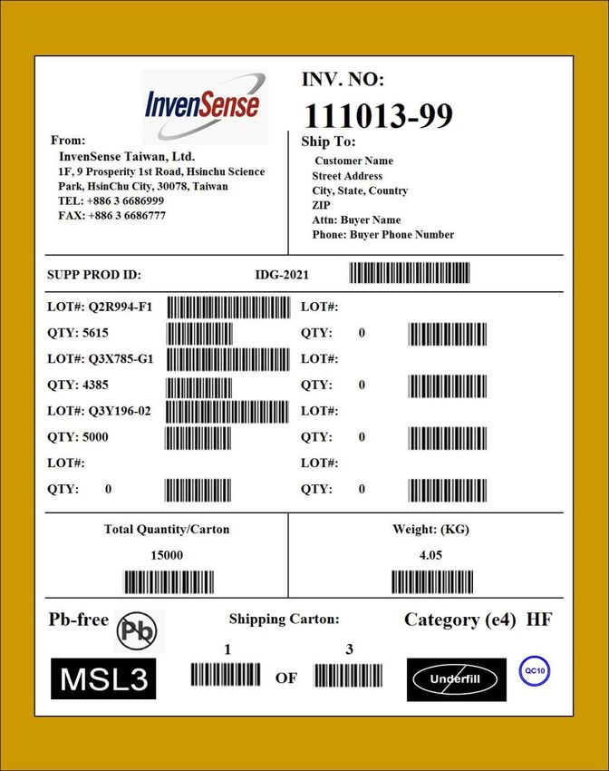
8.10 Representative Shipping Carton Label
Confidential & Proprietary 34 of 36You can also read