IMPACT OF BORON AND INDIUM DOPING ON THE STRUCTURAL, ELECTRONIC AND OPTICAL PROPERTIES OF SNO2 - RESEARCHGATE
←
→
Page content transcription
If your browser does not render page correctly, please read the page content below
Impact of boron and indium doping on the
structural, electronic and optical properties of SnO2
Petros-Panagis Filippatos
National Center for Scienti c Research Demokritos
Dr N Kelaidis
National Center for Scienti c Research Demokritos
Maria Vasilopoulou
National Center for Scienti c Research Demokritos
Dimitris Davazoglou
National Center for Scienti c Research Demokritos
Alexander Chroneos ( alexander.chroneos@imperial.ac.uk )
Imperial College
Research Article
Keywords: tin dioxide (SnO2),optoelectronic devices
DOI: https://doi.org/10.21203/rs.3.rs-393104/v1
License: This work is licensed under a Creative Commons Attribution 4.0 International License.
Read Full License
Page 1/17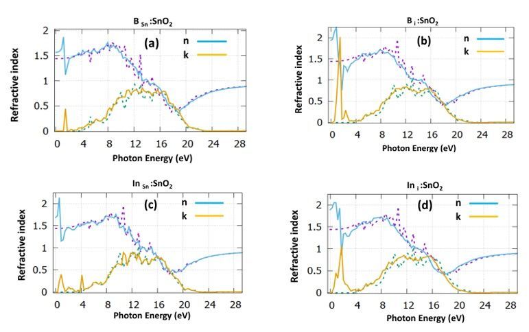
Abstract
Tin dioxide (SnO2), due to its non-toxicity, high stability and electron transport capability represents one
of the most utilized transition metal oxides in many optoelectronic devices such as photocatalytic
devices, photovoltaics (PVs) and light-emitting diodes (LEDs). However, its wide bandgap reduces its
charge carrier mobility and its photocatalytic activity. Doping with various elements is an e cient and
low-cost way to decrease SnO2 band gap and maximize photocatalytic applications' potential. Here, we
apply density functional theory calculations to examine the effect of p-type doping with B and In of SnO2
on its electronic and optical properties. Calculation predict the creation of shallow energy states in the
band gap, near the valence band, when the dopant (B or In) is in interstitial position. In the case of
substitutional doping, a signi cant decrease of the band gap is calculated. We also investigate the effect
of doping on the surface sites of SnO2. We nd that B incorporation in the (110) does not alter the gap
while In causes a notable decrease. The present work highlights the signi cance of boron and indium
doping in SnO2 both for solar cells and photocatalytic applications.

Introduction
Tetragonal SnO2 is a wide bandgap semiconductor which typically shows n-type conductivity due to the
oxygen vacancies that are created during the crystallization process [1–4]. SnO2 is commonly used for
glazes [1], polishing powder [2], photovoltaics[3], ανδ gas sensors [4]. Recently, SnO2 has been
demonstrated as a cathode material in Li-ion batteries [5]. Wang et al. [5] have shown that Sn2O3 in SnO2
nanosheets signi cantly improves battery performance. However, the common SnO2 lms exhibit low
intrinsic carrier mobility, which has been attributed to deep donor states originating from oxygen
vacancies[3]. Many doping strategies have been adopted to further increase its electrical conductivity and
improve its absorption in the visible region –for photocatalytic applications- by reducing its wide energy
gap. Speci cally, many experimental and theoretical works have demonstrated that halogen doping in
SnO2 increases conductivity and transparency, making it a better candidate for optoelectronic
applications [6, 7].

Another option for improving the properties the properties of SnO2 is doping with p-type elements [8].
Transparent conducting oxides (TCOs) fabricated from doped semiconductor oxides such us In:SnO2
(ITO), F:SnO2 (FTO) and B:ZnO (BZO) are commonly used as transparent conductive materials in
industrial applications such as displays and lighting devices [8]. In these structures, the metal atom is
generally substituted by the dopant, which improves the charge carrier conductivity. Experimental reports
on mesoporous oxides indicate remarkable chemical properties when boron in an interstitial position [9].
These boron interstitials enhance the carrier densities of the semiconductors and help to adopt a diverse
coordination environment with abundant oxygen vacancies. Additionally, some reports propose boron as
a doping candidate for SnO2 based photocatalytic applications [10].

                                                   Page 2/17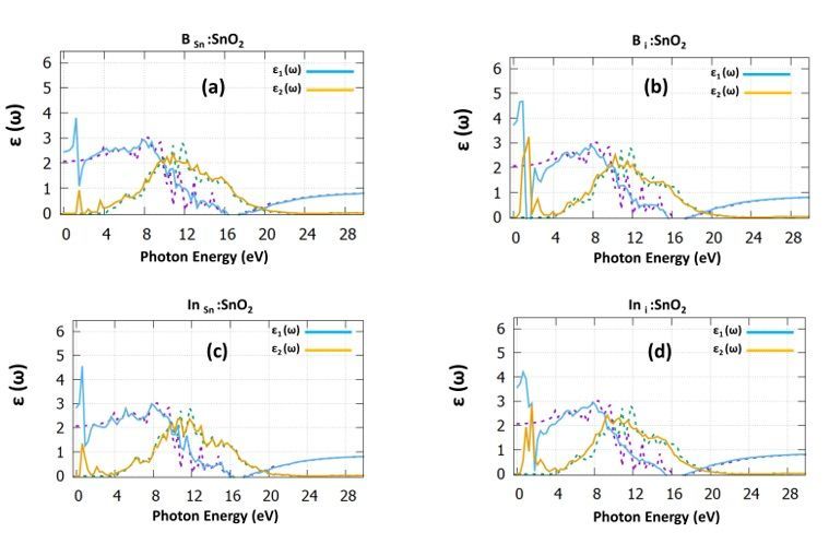
Apart from the experimental works, there are also many theoretical studies based on density functional
theory (DFT) that examine the in uence of doping in SnO2, mostly in substitutional positions [11–17].
Especially for the halogen substitutional doping, it is revealed that single donor states arise inside the
bandgap; however, the effect of interstitials is not generally taken into consideration by the community.

In most previous DFT studies, tin oxide bandgap is underestimated and predicted at a value of 1-2eV [17–
18].    This is a well-known de ciency of the Local Density Approximation (LDA) and of the Generalized
Gradient Approximation (GGA). Therefore, the use of computationally demanding but more accurate
hybrid exchange-correlation functionals are deemed necessary to accurately describe the band gap and
the position of states in the gap or at its edges.

In the present study, we apply Hybrid functional DFT calculations using PBE0 [45] achieve a bandgap
value of 3.35 eV, which agrees well with the experimentally reported prediction [3, 19]. More analytically, we
examine the effect of boron and indium doping on the bulk SnO2 and we also investigate the effect of
interstitial doping of the (110) surface for the rst time. Density of states (DOS) calculations showed a
reduction of the band gap in all cases, which is more profound for the interstitial doping and formation of
energy states in the bandgap for the substitutional doping. This bandgap reduction combined with the
created intergap energy levels are highly bene cial for the photocatalytic applications of SnO2 while the
predicted characteristics can also be applied in photovoltaic technologies.

Results
Bulk rutile SnO2

SnO2 forms in the P42/mmm space group and crystalizes in a rutile structure. The experimental unit cell
parameters a = b = 4.737 Å and c = 3.186 Å were determined using X-ray diffraction (XRD) experiments
[11].   The calculated lattice parameters after the relaxation of rutile SnO2 are a = b = 4.717 Å and c = 3.189
Å in good agreement with the experimental values. The dopant percentage of our calculations is 1 B or In
atom per 48 SnO2 atoms, which results in a 2.08% additional doping. Zhang et al. [20] performed
experiments regarding the effect of boron in tin oxide and they predicted that boron can either substitute
a tin atom or occupy an interstitial position .We predict that for the substitutional case, boron atom
occupies a tin site and is located at a distance of 1.775 Å from the nearest oxygen atom (refer to Fig. 1a)
while for the interstitial case, the boron atom sites at a distance of 1.475 Å from the O-atom (refer to
Fig. 1b). In Figs. 1c and 1d we show the InSn :SnO2 and In i : SnO2 cases, respectively. The substitutional
dopant is relaxed at a distance of 2.11 Å from the nearest oxygen atom, while the interstitial is located at
a distance of 2.03 Å. In Table 1, we report the relevant lattice parameters and volume changes, through
doping, for the bulk system. Concerning the B:SnO2 cases, there is a small decrease in the lattice volume
for the substitutional case, which can be attributed to the smaller ionic radius of B than Sn (B3+:0.23 Å,
Sn4+:0.71 Å) while for the interstitial case, there is an increase. The present results agree with the
available experimental data that predict a decrease of the lattice parameters for the BSn : SnO2 and an
                                                      Page 3/17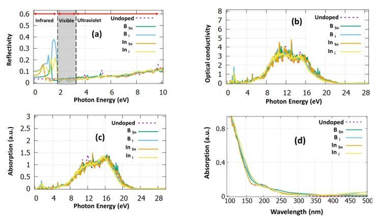
increase for the B i :SnO2 [9]. Similarly for the In:SnO2 we predicted that in all the cases, there is an
increase to the lattice parameters. This agrees with previous experimental studies [21].
Table 1
The calculated lattice constants and cell
volumes for all the dopants.
a(Å) c(Å) Vol ( Å3)
SnO2 4.717 3.189 70.956
B Sn :SnO2 4.674 3.153 68.881
B i :SnO2 4.866 3.225 76.361
In Sn :SnO2 4.730 3.194 71.459
In i :SnO2 4.901 3.220 77.343
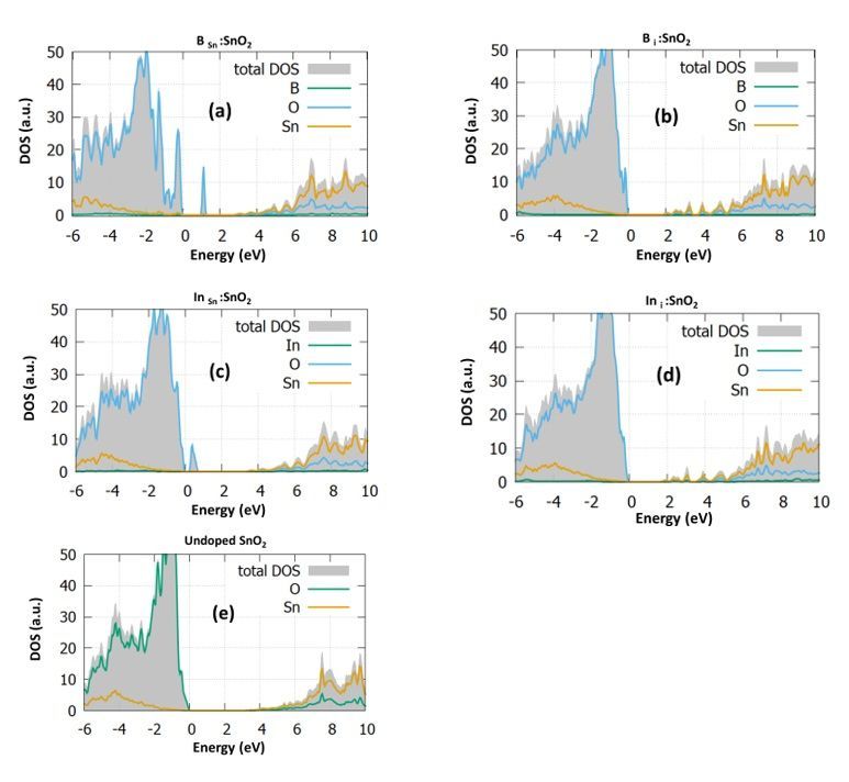
For each doping case, we calculate the DOS and the PDOS and present them in Fig. 2. The DOS of the
undoped SnO2 is illustrated in Fig. 2e for reference. To have a clear and more reliable picture of the
changes of the electronic structure due to doping, we use for our calculations the hybrid functional PBE0,
which provides a good bandgap value for our model (calculated at 3.35eV) and in agreement with
previous theoretical works [7] and the experimental value [19].
In Fig. 2a, the B Sn : SnO2 case is examined. In this case, it is observed from the total DOS (grey) that the
bandgap is reduced to the value of 3eV while some energy states are created inside the bandgap at 1eV.
Furthermore, it is seen that some additional states arise at the valence band maximum. Looking at the
PDOS of the boron substitutional case, we predict that these states are created mostly from the
hybridization of O-2p with Sn-5p and the B-2p orbitals. Our prediction agrees well with the work of Yu et
al. [22], which also predicts mid-gap states and gap reduction when boron is inserted. However, in their
study, there is an underestimation to the bandgap value of tin dioxide. Similar experimental studies [23]
have shown that 2% boron doping reduces the bandgap 0.4 eV, which is identical to the reduction we
predicted.
To further investigate the effect of boron doping, we investigate the effect of interstitial boron in tin oxide.
We expect that the interstitial incorporation of boron results in gap states forming to the conduction band
edge. The bandgap is seen to increase to the value of 3.9 eV. As it is discussed in previous works, the
formation of energy states in the middle of the gas is highly bene cial for photocatalytic applications, but
still, they can be a crucial disadvantage for PV and LED devices as they work as “traps” which reduce the
device photocurrent and the photogenerated charge carriers [24, 25]. Although B i :SnO2 has not been
examined theoretically yet, Zhi et al. [9] predicted that interstitial atomic positions play a signi cant role in
Page 4/17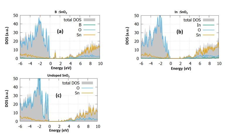
increasing the capacity of tin oxide, making it a good t for supercapacitor applications. In fact, in their
work, they used a 4% doping percentage of boron and they concluded that the interstitial atoms slightly
increased the bandgap. This phenomenon is called the “Moss-Burstein effect” and it is generally seen in
heavily doped semiconductors, where after a doping concentration, the bandgap of the semiconductor
starts to increase even reaches higher values than the undoped material [26]. In the case of Bi :SnO2, this
provides a su cient number of charge carriers that improve the capacitance of SnO2 [27]. We predicted
this bandgap increase both in the case of the bulk SnO2 and in the (110) surface of SnO2. The (110)
plane is considered the most highly energetic plane of the experimental SnO2 structure [9, 28, 29] as we
discuss in the next section and our calculations complete the DFT work of Zhi et al. [9], which gave
emphasis only to the (002) plane.

Continuing with the bulk In:SnO2 we examined the interstitial and substitutional formation again.
Focusing on the DOS of In Sn : SnO2 (Fig. 2c) we predicted again unoccupied energy states near the
valence band at 0.8eV ,which are created due to the hybridization of O-2p with Sn-5p and In-5p. These
gap states might be bene cial for device fabrication as they will serve as a route for the transition from
the valence to the conduction band. Furthermore, it is seen that this time the bandgap is slightly
decreased at a value of 3.25eV. Lastly, we performed calculations for the interstitial doping of indium in
tin oxide. We predict that the In-5p orbitals play a signi cant role in shifting the conduction band and
reducing the band gap, which reaches a value of 1.9 eV. Like the boron case, the interstitial doping does
not give rise to any energy levels inside the gap. The present results agree well with the experimental data
of Abdulsattar et al. [30], which predicted a slight decrease to the bandgap with a doping percentage of
2%. All these results show that although B:SnO2 shows energy states that are detrimental for device
applications, its evident gap reduction makes it possible for photocatalytic applications. In contrast,
In:SnO2 shows characteristics that make it a good candidate for electron transport layer material for
photovoltaic devices.

To consider possible applications of the doped structures, we calculated all the bulk doped cases' optical
properties. Firstly, to describe the absorption and dispersion mechanisms from the occupied to the empty
electron levels, we predicted the dielectric function, presented in Fig. 3. Focusing on the real part of the
dielectric function for the undoped SnO2 (dotted purple), it is seen that it reaches a maximum value of
8.5eV. The negative value at 16.5eV is attributed to the metallic properties of undoped SnO2 [31–32]. The
imaginary part of the dielectric function provides us helpful information regarding the probability of
photon absorption. We calculated that there is a decreasing trend for all the cases due to the Maxwell-
Wagner interfacial polarization [33]. From the undoped SnO2 case (dotted green), two sharp peaks arise
due to the transitions from O-2p to Sn-5p. The dielectric constant of the undoped case is predicted at 2 in
good agreement with previous experimental [31] and theoretical works [32]. Focusing on BSn : SnO2 (refer to
Fig. 3a) case, we predicted the dielectric constant is signi cantly increased to the value 2.5. The major
peak that arises at 1.7eV of the imaginary part can be attributed to the transition of electrons of B-2p and

                                                  Page 5/17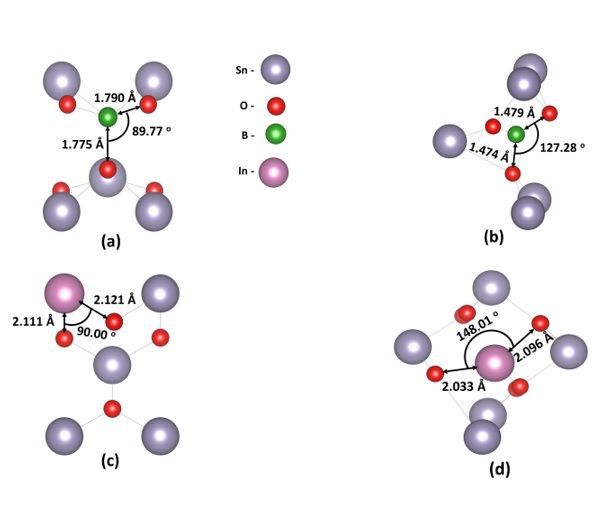
the Sn-5p. Continuing with the interstitial B case (refer to Fig. 3b), there is an evident increase to the
dielectric constant, which reaches a value of 3.8.

Regarding the InSn :SnO2 (Fig. 3c) the dielectric constant is increased to the value of 3, which is
signi cantly higher than the B Sn : SnO2 and nally, for the In i : SnO2 (Fig. 3d) the dielectric constant
reaches the value of 3.7. From Fig. 3 it can also be seen that there is a shift of the low photon energy
peaks towards the visible region accompanied by an increase of the value of the dielectric constant. The
recombination of charge carriers decreases in this kind of material, where the static dielectric constant
monitors the electric elds inside the material by polarization. As a result, both the B i : SnO2 and In i
:SnO2 are highly preferred to use as heterojunction buffer layers in photovoltaic applications.

The refractive index is shown in Fig. 4. For the SnO2 the refractive index is computed in zero frequency at
the value of 1.40, which agrees with other simulation works [32], but it is underestimated compared to the
experimental value of 1.70 [34].

Regarding the doping structures, we predicted a value of 1.55 for the BSn : SnO2 (Fig. 4a), while for the B i
: SnO2 (Fig. 4b), there is an increase reaching a value of 1.95. Looking at the indium doping cases, we
predicted a value of 1.6 for the substitutional case (Fig. 4c) and a value of 1.85 for the interstitial dopant
(Fig. 4d). It is evident that for the refractive index, there is an increase in the lower photon energies and on
contrary, there is a signi cant decrease in the upper energies. This is due to the optical dispersion that
these structures have.

To provide a further insight into the optical properties of all these structures, in Fig. 5 we calculated the
re ectivity, the optical conductivity, and the absorption of the structures. Re ectivity (see Fig. 5a) is one of
the most important properties of these materials because it signi es the amount of photons that are
re ected from the material. We have shown that the values at zero photon energy are calculated at 3%,
5%, 10%, 6% and 9.5% for SnO2, BSn : SnO2, B i : SnO2, In Sn : SnO2 and In i : SnO2 respectively. We
predicted that B : SnO2 has the highest re ectivity in the near-infrared and visible regions compared to all
the other cases. It can also be seen that all the examined cases encounter less that 15% re ectivity in the
infrared and visible region; thus they can be used as antire ective coatings when the dopant
concentration is at 2% [35]. In Table 2 we have gathered all the calculated electrical and optical constants
for reference.

                                                    Page 6/17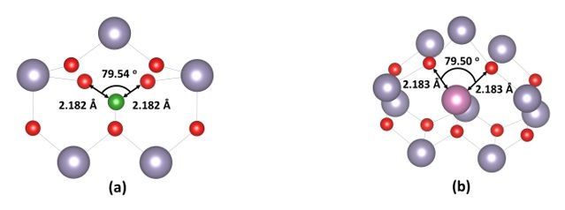
Table 2
                The calculated electronic and optical constants for all the examined cases.
                              Bandgap (eV)       Dielectric constant     Refractive    Re ectivity

                                                                         index

              SnO2            3.33               2.0                     1.40          0.03

              B Sn :SnO2      3.00               2.5                     1.55          0.05

              B i :SnO2       3.90               3.8                     1.95          0.1

              In Sn :SnO2     3.25               3                       1.60          0.06

              In i :SnO2      3.75               3.7                     1.85          0.095

In Fig. 5b we present the optical conductivity of all the calculated structures. If a photon has higher
energy than the optical bandgap then a transition occurs and an electron-hole pair (exciton) is generated.
The mobility of these excitons represent the optical conductivity, which is an important parameter that is
used to design optical detectors [36]. Because of the electronic charge neutrality, these excitons do not
contribute to the electrical conductivity [37]. The highest excitonic features are calculated at 13.2eV for
undoped, B Sn : SnO2 and In Sn : SnO2 cases while for the interstitial dopants they are shifted to 9eV and
10eV for the B and In, respectively. The optical conductivity also describes the losses for a wave with the
same frequency. From the graph, we can conclude that SnO2 and In i :SnO2 have lower losses than the
other cases. Lastly, in Fig. 5c and 5d we present the absorption co-e ciency. The undoped case's
absorption starts at 380nm, which is underestimated compared to the experimental value, which is
approximately 400nm [38]. It is seen that In i and B i have the highest absorption to the visible region.

From the above, we can conclude that both B i and In i exhibit interesting characteristics, making them
applicable to photovoltaic and photocatalytic devices.
Surface (110) of rutile SnO2

As Zhi et al. [9] indicated in their work, to further understand the effect of boron interstitial, the surface of
SnO2 should be examined. For applicable photocatalytic materials with a visible light response and high
charge mobility, such as tin dioxide, attention to the high-energy surfaces should be paid when the
structure is doped with atoms or molecules. However, it is seen that the studies of SnO2 surface are
signi cantly less than the studies of the bulk and they primarily focus on sensor applications of tin oxide
[39]
   . In this section, the change to the electronic properties of B and In doped SnO2 will be investigated and
discussed. Here we used a slab model with a vacuum of 12 Å thickness across the (110) plane. We chose
this particular surface because it is the most intense crystallization plane [9, 39] of the rutile SnO2 and it
has never been studied before regarding the B or In doping. Furthermore, as the (110) plane is one of the

                                                       Page 7/17
most highly energetic surfaces, it will play the role of the active site in photocatalytic reactions [40]. For
our DOS and pDOS calculations we used hybrid calculations again.
In Figs. 6a-6b we present the Bi :SnO2 and In i : SnO2 doping cases. It is seen that the boron interstitial
displaces the tin atom and occupies a tin site to minimize its energy (Fig. 6a). We predicted that
interstitial boron sites at 2.182 Å from the nearest oxygen atom and 3.10 Å from the nearest tin atom. On
the other hand, we calculated that indium atom sites at a distance of 2.183 Å from the nearest oxygen
atom and 3.32 Å from the nearest tin atom. Looking at the DOS and the pDOS of Fig. 7a, it is seen that
boron interstitial produces a small band peak at 1eV.
Interestingly in this high-energy plane the bandgap isn’t decreased compared to the undoped (see Fig. 7c).
We believe that this result combined with the bulk Bi :SnO2 explains the experimental phenomenon that
Zhi et al [9] discussed in their paper about Bi. Looking at the In i : SnO2 (refer to Fig. 7b) we can see that
the (110) surface bandgap decreases to 2eV. The gap of the undoped (110) SnO2 is shown in Fig. 7c at
2.5eV, a good agreement with other DFT works [41]. All the above results indicate that In doping in the
SnO2 shows good characteristics that should be examined in photocatalytic applications.
Conclusions
Herein, we applied DFT calculations for boron and indium rutile SnO2 bulk and surface to evaluate the
doping effect on the electronic and optical properties. Speci cally, we performed DOS calculations and
we found that the bulk structures have a bandgap increase and in the case of boron mid gap states are
formed. Although these states might be detrimental for photovoltaics as they may act as trap states for
photogenerated carriers, they can be the working horse for photocatalytic applications based on B:SnO2.
Our work explains some of the phenomena that have been experimentally observed and open the road for
applications of boron structures to more applications such as supercapacitors. Regarding the indium
defect, we predicted that at low concentrations highly wanted states are formed near the valence band
which can bene cial for energy harvesting devices. Furthermore, its optical characteristics and the
bandgap reduction at the surface make it a worthy candidate for photocatalysis.
Methodology
All our results are based on the Cambridge Serial Total Energy Package (CASTEP) [42–43]. For our
calculations we used the hybrid functional PBE0 in order to consider the effect of the localized electrons
and the bandgap underestimation that is generally encountered in GGA and LDA [44]. The cutoff energy
was chosen at 800eV after performing the convergence test and for our calculations we used an 48 atom
supercell with 2x2x3 k-points for the sampling of the Brillouin zone during the geometry optimization [44].
For the DOS calculations we used a k-point mesh of 5x5x5 for the bulk modelling while for the surface we
applied a 3x3x1 set. Finally, the convergence criteria for our simulations were chosen at 2.0 ∙ 10−
Page 8/175
eV/atom for the SCF tolerance, 0.05 eV/Å for the force tolerance and 0.001Å for the Max displacement
tolerance.
Declarations
Acknowledgements
P.P.F., M.V., D.D. and A.C. are grateful for LRF ICON funding from the Lloyd’s Register Foundation, a
charitable foundation helping to protect life and property by supporting engineering-related education,
public engagement and the application of research. N.K. acknowledges support from European Union’s
H2020 Programme under Grant Agreement no 824072- HARVESTORE.
Contributions
P.P.F. and N.K. performed the calculations. P.P.F., N.K., M.V., D.D. and A.C. contributed to the interpretation
of the results and the writing of the paper.
References
1. Searle, A. B. The Glazer’s Book.London : The Technical Press, 1935.
2. Holleman, A. F. & Wiberg, E.. Inorganic Chemistry, Academic Press. Berlin/New York, (2001).
3. Greenwood, N. N. & Earnshaw, A. Chemistry of the Elements. Elsevier (2012).
4. Tountas, M., Topal, Y., Kus, M., Ersöz, M., Fakis, M., Argitis, P. & Vasilopoulou, M. Water‐Soluble
Lacunary Polyoxometalates with Excellent Electron Mobilities and Hole Blocking Capabilities for
High E ciency Fluorescent and Phosphorescent Organic Light Emitting Diodes. Funct. Mater.,
26(16), 2655-2665 (2016).
5. Wang, C., Du, G., Ståhl, K., Huang, H., Zhong, Y. & Jiang, J. Z. Ultrathin SnO2 nanosheets: oriented
attachment mechanism, nonstoichiometric defects, and enhanced lithium-ion battery performances.
J. Phys. Chem. C 116(6), 4000-4011 (2012).
. Rakhshani, A. E., Makdisi, Y. & Ramazaniyan, H. A. Electronic and optical properties of uorine-doped
tin oxide lms. Appl. Phys. 83(2), 1049-1057 (1998)
7. Filippatos, P.P., Kelaidis, N., Vasilopoulou, M., Davazoglou, D. & Chroneos, A. Defect Processes in
Halogen Doped SnO2. Sci., 11(2), 551 (2021).
. Minami, T. Transparent conducting oxide semiconductors for transparent electrodes. Semicond. Sci.
Technol. 20, S35–S44 (2005).
9. Zhi, J., Zhou, M., Zhang, Z., Reiser, O. & Huang, F. Interstitial boron-doped mesoporous semiconductor
oxides for ultratransparent energy storage. Commun. 12(1), 1-12 (2021).
10. Kong, X.B., Li, F., Qi, Z.N., Qi, L. & Yao, M.M., 2017. Boron-doped tin dioxide lms for environmental
applications. Rev. Lett., 24(05), 1750059 (2017).
Page 9/1711. Peng-Fei, L., Yue, S., Zhong-Yuan, Y., Long, Z., Qiong-Yao, L. , Shi-Jia, L.M., Li-Hong, H. & Yu-Min,L.;
Electronic structure and optical properties of antimony-doped SnO2 from rst-principle study.
Commun. Theor. Phys. 57, 145 (2012)
12. Canestraro, C.D., Roman, L.S. & Persson, C. Polarization dependence of the optical response in SnO2
and the effects from heavily F doping, Thin Solid Films, 517(23), 6301–6304 (2009).
13. Rivera, R., Marcillo, F., Chamba, W., Puchaicela, P. & Stashans, A. SnO2 physical and chemical
properties due to the impurity doping. Lect. Notes Eng. Comp., 2, 814–818 (2013).
14. Velikokhatnyi, O.I. & Kumta, P.N., Ab-initio study of uorine-doped tin dioxide: A prospective catalyst
support for water electrolysis. Physica B, 406(3), 471–477 (2011).
15. Golovanov, V., Golovanova, V., Kuisma, M. & Rantala, T.T. Electron spin resonance parameters of
cation vacancies in tin dioxide doped with uorine and hydrogen. J. Appl. Phys., 114(14), 143907
(2013).
1 . Oshima, M. & Yoshino, K. Structural and Electronic Structure of SnO2 by the First-Principle Study.
Trans Tech, Stäfa, 725, 265–268 (2012).
17. Govaerts, K., Partoens, B. & Lamoen, D. Extended homologous series of Sn–O layered systems: A
rst-principles study. Solid State Comm. 243, 36-43 (2016).
1 . Perdew, J. P. & Levy, M. Physical content of the exact Kohn-Sham orbital energies: band gaps and
derivative discontinuities. Phys. Rev. Lett. 51(20), 1884 (1983).
19. Zervos, M., Lathiotakis, N., Kelaidis, N., Othonos, A., Tanasa, E. & Vasile, E. Epitaxial Highly Ordered
Sb:SnO2 Nanowires Grown by the Vapor Liquid Solid Mechanism on m-, r- and a-Al2O3. Nanoscale
Adv. 1, 1980−1990 (2019).
20. Zhang, B., Tian, Y., Zhang, J.X. & Cai, W.,. The structural and electrical studies on the Boron-doped
SnO2 lms deposited by spray pyrolysis. Vacuum, 85(11), 986-989 (2011).
21. Lekshmy, S.S. & Joy, K. Structural and optoelectronic properties of indium doped SnO2 thin lms
deposited by sol gel technique. Mater. Sci. Mater. Electron., 25(4), 1664-1672 (2014).
22. Yu, J., Wang, Y., Huang, Y., Wang, X., Guo, J., Yang, J. & Zhao, H. Structural and electronic properties
of SnO2 doped with non-metal elements J Nanotech., 11(1), 1321-1328 (2020).
23. Tran, Q.P., Fang, J.S. & Chin, T.S., 2016. Optical Properties and Boron Doping-Induced Conduction-
Type Change in SnO2 Thin Films. Electron. Mater. 45, 349–356 (2016)
24. Filippatos, P. P., Kelaidis, N., Vasilopoulou, M., Davazoglou, D., Lathiotakis, N. N. & Chroneos, A. Defect
processes in F and Cl doped anatase TiO2. Sci Rep 9, 19970 (2019).
25. Filippatos, PP., Soultati, A., Kelaidis, N., Petaroudis, C., Alivisatou, A.A., Drivas, C., Kennou, S., Agapaki,
E., Charalampidis, G., Yusoff, Abd. R. M., Lathiotakis, N. N., Coutsolelos A.G., Davazoglou, D.,
Vasilopoulou, M. & Chroneos, A. Preparation of hydrogen, uorine and chlorine doped and co-doped
titanium dioxide photocatalysts: a theoretical and experimental approach. Sci Rep11, 5700 (2021)
2 . Butcher, K., Hirshy, H., Perks, R. M., Wintrebert, M. & Chen, P. P. T. Stoichiometry effects and the Moss-
Burstein effect for InN. Status Solidi A203, 66–74 (2006)
Page 10/1727. Simon, P. & Gogotsi, Y. Materials for electrochemical capacitors. Mater.7, 845–854 (2008).
2 . Kumar, M., Kumar, A. & Abhyankar, A.C. SnO2 based sensors with improved sensitivity and response‐
recovery time. int, 40(6), 8411-8418 (2014).
29. Manassidis, I., Goniakowski, J., Kantorovich, L.N. & Gillan, M.J. The structure of the stoichiometric
and reduced SnO2 (110) surface. Sci., 339(3), 258-271 (1995).
30. Abdulsattar, M.A., Batros, S.S. & Addie, A.J. Indium doped SnO2 nanostructures preparation and
properties supported by DFT study. Superlattices Microstruct.100, 342-349 (2016).
31. Tingting, S., Fuchun, Z., & Weihu, Z. Density functional theory study on the electronic structure and
optical properties of SnO2. Rare Metal Mat. and Eng., 44(10), 2409-2414 (2015).
32. Khan, A.F., Mehmood, M., Aslam, M. & Ashraf, M. Characteristics of electron beam evaporated
nanocrystalline SnO2 thin lms annealed in air. Appl. Surf. Sci., 256(7), 2252-2258 (2010)
33. Singh, A., Chatterjee, R., Mishra, S.K., Krishna, P.S.R. & Chaplot, S.L. Origin of large dielectric constant
in La modi ed BiFeO3-PbTiO3 multiferroic, J. Appl. Phys. 111 (1), 014113 (2012).
34. A fy, H.H, Momtaz, R.S., Badawy, W.A. & Nasser, S.A. Some physical properties of uorine-doped
SnO2 lms prepared by spray pyrolysis. J. Mater. Sci. Mater. Electron., 2(1), 40-45 (1991).
35. Khoshman, J.M. & Kordesch, M.E. Optical properties of a-HfO2 thin lms. Surf. Coating. Technol. 201
(6), 3530–3535 (2006).
3 . Akinlami, J.O. & Olateju, I.O. Re ection coe cient and optical conductivity of gallium nitride GaN.
Electron. Optoelectron. 15 (3), 281-284 (2012).
37. Dash, L.K., Vast, N., Baranek, P., Reining, M.C. & Cheynet, L. Electronic structure and electron energy-
loss spectroscopy of ZrO2 Phys. Rev. B 70 (24), 245116 (2004).
3 . Doyan, A., Susilawati & Imawanti, Y.D. Synthesis and Characterization of SnO2 thin layer with a
doping Aluminum is deposited on Quartz Substrates. AIP AIP Conf. Proc, 1801 (1), 020005 (2017).
39. Wang, X., Qin, H., Chen, Y. & Hu, J. Sensing mechanism of SnO2 (110) surface to CO: density
functional theory calculations. Chem. Phys C 118(49), 28548-28561 (2014).
40. Talebian, N. & Jafarinezhad, F. Morphology-controlled synthesis of SnO2 nanostructures using
hydrothermal method and their photocatalytic applications. Int. 39(7), 8311-8317 (2013).
41. Li, M., Zhu, H., Wei, G., He, A. & Liu, Y. DFT calculation and analysis of the gas sensing mechanism of
methoxy propanol on Ag decorated SnO2 (110) surface. RSC Adv., 9(61), 35862-35871 (2019).
42. Segall, M. D., Lindan, P. J., Probert, M. A., Pickard, C. J., Hasnip, P. J., Clark, S. J. & Payne, M. C. First-
principles simulation: ideas, illustrations and the CASTEP code. J. Phys. Cond. Matter, 14(11), 2717-
2744 (2002).
43. Ceperley, D. M. & Alder, B. J. Exchange-correlation potential and energy for density-functional
calculation. Phys. Rev. Lett 45, 567-581 (1980).
44. Paier, J., Marsman, M., Hummer, K., Kresse, G., Gerber, I. C. & Angyan, J. G. Screened hybrid density
functionals applied to solids. J. Chem. Phys. 124, 154709 (2006).
Page 11/1745. Ernzerhof, M. & Scuseria, G. E. Assessment of the Perdew–Burke–Ernzerhof exchange-correlation
functional. Chem. Phys., 110(11), 5029-5036. (1999).
Figures
Figure 1
The structures of (a) Boron substitutional doped SnO2 (B Sn : SnO2), (b) Boron interstitial doped SnO2 (B
i : SnO2), (c) Indium substitutional doped SnO2 (In Sn : SnO2) and (d) Indium interstitial doped SnO2 (In i
: SnO2).
Page 12/17Figure 2
The total density of states (DOS) and the projected density of states (PDOS) of (a) B Sn : SnO2, (b) B i :
SnO2, (c) In Sn : SnO2, (d) In i : SnO2 and (e) undoped SnO2.
Page 13/17Figure 3
The dielectric function for (a) B Sn : SnO2, (b) B i : SnO2, (c) In Sn : SnO2 and (d) In i : SnO2. The dotted
purple and dotted green, correspond to the dielectric function of the undoped SnO2
Page 14/17Figure 4
The refractive index for (a) B Sn : SnO2, (b) B i : SnO2, (c) In Sn : SnO2 and (d) In i : SnO2. The dotted
purple and dotted green, correspond to the dielectric function of the undoped SnO2
Page 15/17Figure 5
(a) The re ectivity for all the doped structures (b) The optical conductivity for all the studied structures (c)
the absorption coe cient for all the structures versus the photon energy (d) the absorption coe cient for
all the structures versus the wavelength. The dotted purple and dotted green, correspond to the undoped
SnO2 .
Figure 6
The structures of (a) Boron doped (110) SnO2 surface and (b) Indium doped (110) SnO2 surface.
Page 16/17Figure 7
The total density of states (DOS) and the projected density of states (PDOS) of (a) B (b) In and (c)
Undoped (110) SnO2 surface.
Page 17/17You can also read