Integrated impedance bridge for absolute capacitance measurements at cryogenic temperatures and finite magnetic fields
←
→
Page content transcription
If your browser does not render page correctly, please read the page content below
Integrated impedance bridge for absolute capacitance measurements at
cryogenic temperatures and finite magnetic fields
G.J. Verbiest,1, 2 H. Janssen,1 D. Xu,1, 3 X. Ge,1 M. Goldsche,1, 4 J. Sonntag,1, 4 T. Khodkov,1, 4 L. Banszerus,1, 4
N. von den Driesch,4 D. Buca,4 K. Watanabe,5 T. Taniguchi,5 and C. Stampfer1, 4
1)
JARA-FIT and 2nd Institute of Physics, RWTH Aachen University, 52056 Aachen, Germany,
EU
2)
Current address: 3mE, Delft University of Technology, 2628 CD Delft, The Netherlands,
EU
3)
QuTech and Kavli Institute of Nanoscience, Delft University of Technology, 2600 GA Delft, The Netherlands,
EU.
4)
Peter Grünberg Institute (PGI-8/9), Forschungszentrum Jülich, 52425 Jülich, Germany,
EU
5)
arXiv:1901.05769v2 [physics.ins-det] 27 Jun 2019
National Institute for Materials Science, Tsukuba, Ibaraki 305-0047, Japan
We developed an impedance bridge that operates at cryogenic temperatures (down to 60
mK) and in perpendicular magnetic fields up to at least 12 T. This is achieved by mounting
a GaAs HEMT amplifier perpendicular to a printed circuit board containing the device under
test and thereby parallel to the magnetic field. The measured amplitude and phase of the
output signal allows for the separation of the total impedance into an absolute capacitance
and a resistance. Through a detailed noise characterization, we find that the best resolution
is obtained when operating the HEMT amplifier √ at the highest gain. We obtained a reso-
lution in the absolute capacitance of 6.4 aF/ Hz at 77 K on a comb-drive actuator, while
maintaining a small excitation amplitude of 15 kB T /e. We show the magnetic field func-
tionality of our impedance bridge by measuring the quantum Hall plateaus of a top-gated
hBN/graphene/hBN heterostructure at 60 mK with a probe signal of 12.8 kB T /e.
I. INTRODUCTION Hove singularities in carbon nanotubes, a probe signal on
the order of the characteristic thermal energy kB T /e is
required.13 However, bridge circuits and LCR meters usu-
Electronic and electromechanical devices are charac-
ally include some lengthy cables which give rise to a par-
terized by an impedance that defines their functionality.
asitic capacitance in the order of hundreds of picofarads.
Thus, an accurate measurement system for impedances
This large parasitic capacitance results in a huge atten-
is thus of crucial importance to develop, characterize,
uation of the probe signal which, in combination with
and optimize electronic and electromechanical devices.1
the required kB T /e excitation, pushes attofarad capaci-
Impedances are commonly measured with bridge circuits
tance changes below the resolution limit. To reduce the
or LCR-meters. The ongoing miniaturization of elec-
effect of the parasitic capacitance of the cables, Hazeghi
tronic and electromechanical devices push these measure-
et al. used a high-electron mobility transistor (HEMT)
ment techniques to the limit. For example, the density of
as an impedance-matching amplifier in an integrated√ ca-
available electronic states in nanostructures becomes fi-
pacitance bridge.9,10,15,25
√ A resolution of 60 aF/ Hz at
nite which results in a so-called quantum capacitance3,4
or the displacement of electromechanical devices enter 300 K and 21 aF/ Hz at 4.2 K was achieved on a top-
the nanoscale.5,6 Both these examples result typically in gated graphene device with probe signals on the order of
capacitance changes of only a few aF. Standard mea- kB T /e. However, a problem arises if the density of states
surement techniques cannot resolve these changes due to approaches zero. As Cq approaches zero, also the con-
parasitic impedances arising from lengthy cables connect- ductance approaches zero due to the absence of charge
ing the device under test (DUT) and the measurement carriers. Depending on the frequency of the probe sig-
system. nal, the measured signal becomes a function of both and
thus depends on the total impedance.
Direct measurements of the density of states via the
quantum capacitance have been successful for among In this work, we expand the previously reported inte-
others, graphene7–15 and carbon nanotube16 devices as grated capacitance bridge25 into an integrated impedance
well as GaAs-based devices containing a two-dimensional bridge to determine not only the absolute capacitance
(2D) electron gas.17,18 In such systems with a low den- but also the resistance. We achieve this by performing a
sity of states the total capacitance needs to be expressed thorough analysis, including noise optimization, of both
by the quantum capacitance Cq in series to the geo- the amplitude and the phase of the measured signal. Our
metric capacitance Cg leading to a total capacitance work differs at four additional points from existing litera-
Ctot = Cq Cg /(Cq +Cg ), which is also strongly depending ture: (i) we place the HEMT perpendicular on a printed
on the density of states. Measurements of this quantity circuit board (PCB) to allow for magnetic field depen-
were performed with a bridge circuit,19–23 a LCR meter, dent measurements, (ii) we use a much smaller refer-
or even a scanning tunneling microscope.24 The latter ence resistor to operate the bridge at higher frequencies,
provides local information whereas the former charac- (iii) we show that the impedance bridge operates at tem-
terizes the entire device. In order to fully resolve fine peratures down to 60 mK, and (iv) we show through a
features in their electronic bandstructure such as van detailed noise characterization that the best impedance
2

       (a)                                 Output Circuit           matching amplifier.25 The HEMT in our bridge is a pack-
                                              Vdd                   aged FHX35LG transistor26 with a gate capacitance of
                       Bridge Circuit                               ∼0.5 pF that is part of a small remaining parasitic ca-
                                                Rload               pacitance Cpar . A gate bias Vref of -1 V fully depletes the
                                                                    2D electron gas in the GaAs-based HEMT.
                           Cpar            D
                                                        vout           The reference resistor Rref is used to balance the sig-
       Vref Bias Tee     Rref         G                                                                              −1
                                                                    nal across the unknown impedance ZDUT = YDUT         , where
                                           S                        YDUT is the corresponding admittance of the device un-
                          YDUT                                      der test (DUT). As the HEMT gate (G) is biased through
               vref                                                 Rref , Rref should be much smaller than the HEMT DC
                       vDUT
                                                                    gate resistance across all temperatures. In addition, Rref
                                     Bias Tee                       forms together with Cpar and the capacitive contribution
                                                                    of ZDUT , a low-pass filter. We choose Rref equal to the
                                    VDUT                            impedance of the expected ZDUT parallel to a parasitic
       (b)                                                          capacitance Cpar at the measurement frequency to pre-
                              DUT     HEMT                          vent additional shunting of the signal across ZDUT . To
               10 mm
                                                            B       satisfy these constraints and to maximize the bandwidth,
                                                                    we use a reference resistance Rref of 1 MΩ with a low
                                                                    temperature coefficient (SMD type thick film resistor).
                                                                       The output circuit (see Fig. 1a) consists of a load re-
                                                                    sistor Rload and the drain (D) to source (S) resistance of
       (c)                              Rload                       the HEMT. Rload is used to bias the HEMT drain with
                           vout                  Vdd
                                                                    the voltage Vdd . To ensure stable operation, Rload must
                                                                    be larger than the resistance of the cables. Therefore,
                                                Rref                we choose a Rload = 1 kΩ. The maximum amplifica-
       VDUT                                                         tion is expected when the drain-source resistance of the
                                                Vref
                                                                    HEMT is roughly equal to Rload . We always place Rload
       +vDUT                                    +vref               at room temperature to minimize the heat load of the
                                                                    output circuit. While measuring in a dilution refrigera-
                                                                    tor (a Triton 200 system), the temperature, as measured
                                                        HEMT        with a built-in calibrated RuO2 sensor, increased from
                                                                    15 mK to 50 mK when biasing the HEMT drain with
FIG. 1. (a) Schematic overview of the measurement circuit,          Vdd = 0.55 V.
which consists of a bridge circuit and an output circuit that
                                                                       For successful operation of the circuit in a perpendic-
are coupled via a HEMT amplifier. The bridge circuit con-
tains a reference resistor of 1 MΩ, a parasitic capacitance Cpar
                                                                    ular magnetic field, we place the HEMT on a small PCB
to ground, and an unknown admittance YDUT . The output              that is mounted perpendicular to the PCB containing
circuit has a load resistor of 1 kΩ and an output line for Vout .   Rref and ZDUT (see Fig. 1(b) and (c)). The electrical con-
The bias tees used for summing the AC and DC signal (blue)          nections to the PCB are made via SMP thru hole PCB
are not on the PCB. (b) A side view (optical image) of the          mounts. We characterized both Rref and the HEMT in a
PCB shows the perpendicular placement of the HEMT on                Triton 200 system at mK temperatures for different ap-
the PCB, which allows for measurements at high magnetic             plied magnetic fields. Rref is approximately 0.98 MΩ at
fields. (c) top view (optical image) of the PCB including the       room temperature and 1.03 MΩ at 30 mK. Both values
placement of the different components and the electrical con-       are within the 3% tolerance given by the manufacturer.
nections.                                                           As Fig. 2a shows, Rref only changes by 0.1% when ap-
                                                                    plying a magnetic field of 12 T perpendicular to the PCB
                                                                    containing Rref . Similarly, the operation of the HEMT re-
resolution is obtained when operating the HEMT at its
                                                                    mains unaffected when a magnetic field is applied parallel
highest amplification.
                √       Ultimately, we achieve a resolu-
                                                                    to the drain-source channel of the HEMT (see Figs. 2b
tion of 6.4 aF/ Hz at a temperature of 77 K. To show
                                                                    and 2c). We conclude that the resulting Lorentz forces
the magnetic field applicability of our circuit, we mea-
                                                                    acting on the 2D electron gas have no effect and thus that
sure the quantum Hall plateaus emerging in a top-gated
                                                                    the integrated impedance bridge remains fully functional.
hBN/graphene/hBN heterostructure in magnetic fields
up to 12 T at 60 mK.                                                   In operation, two AC signals at the same frequency are
                                                                    used, of which one is sent through a reference resistance
                                                                    Rref (vref ) and one through the DUT (vDUT ). The am-
                                                                    plitude and phase of these signals are set such that they
II.   BRIDGE DESIGN AND OPERATION
                                                                    interfere destructively at the so-called bridge point at the
                                                                    gate of the HEMT. The signal vb at the bridge point is
  The bridge circuit (see Fig. 1a) consists of a reference          an average of the applied AC signals vref and vDUT ,
resistor and an impedance-matching amplifier to elimi-
nate the effect of large parasitic cable capacitances. To
ensure functionality of the bridge down to cryogenic tem-                               YDUT · vDUT + Yref · vref
                                                                                 vb =                             ,         (1)
peratures, we use a (GaAs-based) HEMT as impedance-                                       Yref + YDUT + Ypar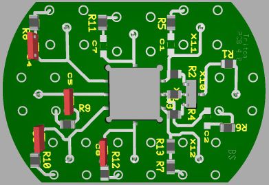
3

 (a)                                                                              If YDUT is a pure capacitor, the minimal detectable
Rref (MΩ)       1.04
                                                                  T=30 mK         change δCDUT in CDUT is therefore given by
                1.03
                                                                                                                  vnoise
                1.02                                                                              δCDUT =                     ,              (4)
                       0               4               8                12                                    |AHEMT · ω · S|
                                       Magnetic Field (T)
 (b)               1                                                              where vnoise is the spectral density of the voltage noise
                                                                                  arriving at the input stage of the lock-in amplifier and ω
                 0.8                                                              is 2π times the measurement frequency.
                                                                                     For the optimization of the resolution to determine
  Vout (V)

                 0.6
                                                                                  YDUT , we used a voltage controlled capacitor (SVC70427 )
                 0.4        T=50mK, B=9T, Vdd=550mV
                                                                                  as DUT. These measurements were performed at room
                                                                                  temperature. All measurements in this work were per-
                 0.2        T=50mK, B=0T, Vdd=550mV
                                                                                  formed at 100 kHz. The required bias potentials were
                           T=RT, B=0T, Vdd=1000mV
                   0                                                              applied with Yokogawa 7651 DC sources. The output
 (c)                                                                              of the bridge circuit was measured with a Zurich Instru-
                   0
                                                                                  ments lock-in amplifier (model UHF). As we did not ob-
                                                                                  serve any phase shifts in vout , we model YDUT with a
  dVout/dVref

                  -1
                                                                                  capacitance CDUT . We balanced the bridge at four dif-
                  -2                                                              ferent VDUT and extracted CDUT according to Eq. (2)
                                                                                  and Cpar from the vref dependence of Eq. (1). The data
                  -3                                                              points in Fig. 3a show that Cpar is four times bigger than
                                                                                  the gate capacitance of the HEMT, which indicates a
                   -1          -0.8      -0.6      -0.4        -0.2         0     significant contribution coming from the PCB itself. We
                                            Vref (V)                              also swept VDUT for five different pairs of vref and vDUT
                                                                                  while recording vout and translated this into CDUT using
                                                                                  Eq. (1). As depicted in Fig. 3a, the extracted capac-
FIG. 2. (a) The measured reference resistance Rref as a func-                     itances from all the different measurements are in ex-
tion of magnetic field at 30 mK. Comparing the value at
                                                                                  cellent agreement with one another. The absolute val-
B = 12 T with the one at 0 T indicates a negligible change
of 0.1%. (b) DC output signal Vout as a function of the ap-                       ues are also in good agreement with the datasheet of
plied DC potential Vref on the gate of the HEMT and (c) the                       the voltage controlled capacitor.27 Now confident that
derivative of (b) with respect to Vref , which defines the gain                   our bridge circuit gives reproducible data, we balanced
of the HEMT. We observe a change when going from room                             the circuit at VDUT = 10 V and fixed vref and vDUT .
temperature (RT) to 50 mK, but a negligible difference be-                        Then, we measured vout as a function of VDUT for dif-
tween the curves at 0 T and 9 T, which are both taken at 50                       ferent HEMT amplifications AHEMT . At each VDUT , we
mK.                                                                               recorded 100 points with a rate of 1 point/s to estimate
                                                                                  the noise in vout and thus in CDUT . We define the resolu-
                                                                                  tion as the √ root-mean-square value of the noise in CDUT
where Yref , YDUT , and Ypar are the admittances of Rref ,                        divided by BW , where BW is the measurement band-
ZDUT , and Cpar , respectively. When balanced (vb =                               width. Figure 3b shows that the resolution in capaci-
0 V), the amplitude and phase of YDUT are given by                                tance is best for the highest HEMT amplification and
                                                                                  lowest CDUT . Both results are understood when consid-
                                                                                  ering Eq. (4). The highest HEMT amplification directly
                                           YREF · vREF                            minimizes δCDUT whereas the lowest CDUT maximizes
                               YDUT = −                .                    (2)
                                             vDUT                                 S (see Eq. (3)) and thereby minimizes δCDUT . The for-
                                                                                  mer directly implies that the circuit is not limited by the
As YDUT is the only quantity that is tunable with the DC                          voltage noise vnoise arriving at the bridge point, as this
voltage VDUT , we need to characterize the other admit-                           would be amplified by the HEMT as well. We find that
tances in the circuit only once. The signal vb is ampli-                          the measured vnoise is approximately equal to the John-
fied AHEMT times by the HEMT into the output voltage                              son noise of the 1 MΩ input resistance of the lock-in am-
vout = AHEMT · vb , which is measured with a lock-in am-                          plifier. Strikingly, the resolution improves by two orders
plifier. The output voltage vout is in all measurements                           of magnitude when increasing VDUT from 0 V to 10 V
below 0.5 mV, which allows us to neglect any nonlinear                            (see Fig. 3). As Eq. (3) shows, the sensitivity S scales
contribution from the HEMT transduction to AHEMT .                                         −2
                                                                                  with CDUT    , if |YDUT | is (much) larger than |Yref + Ypar |.
The measured amplitude and phase of the output volt-                              Considering this scaling relation and the measured CDUT
age vout is used in Eq. (1) to compute the unknown YDUT .                         values depicted in Fig. 3a, the observed improvement in
The sensitivity S of the circuit to a change in YDUT is                           resolution is in agreement with the decrease by one order
given by the derivative of Eq. (1) with respect to YDUT                           of magnitude in CDUT .
                                                                                     To explore the limits of the achievable resolution with
                                                                                  the bridge circuit, we performed measurements on a de-
                            Yref · (vDUT − vref ) + Ypar · vDUT                   vice with a negligible |YDUT | compared to |Yref + Ypar |
                       S=                                  2      .         (3)
                                  (Yref + YDUT + Ypar )                           such that the sensitivity S becomes independent from
4

(a)                       50                                                                  plifier (model SR830). The measurement was performed
                                                        CDUT   (vref, vDUT)                   with a small vDUT of 88.9 µV or 15 kB T /e (frequency of
                          40                                   (25 mV, 1 mV)
                                                        Cpar                                  100 kHz). We did not observe any phase shifts in vout
                                                               (51 mV, 2 mV)
  CDUT (fF)

                          30                                                                  and thus model YDUT with only a capacitance CDUT . As
                                                               (58.34 mV, 2 mV)
                          20                                   (58.34 mV, 2.305 mV)           Fig. 4c shows, the capacitance of this device is 73 fF and
                                                               (67.57 mV, 2.312 mV)           increases to 79 fF at VDUT = 5 V. We determined Cpar
                          10                                                                  to be 6.5 pF using the same method as for the voltage
                           0
                                                                                              controlled capacitance discussed above. The capacitance
(b)                                                                                           is a few tens of fF higher than the one from the par-
                         100                                                                  allel plate approximation for the interdigitated fingers
                                                                              A HEMT =
   Resolution (fF/√Hz)

                                                                                  0.02        due to additional capacitances coming from stray fields,
                                                                                  0.26        bond wires, and other parts of the comb-drive actuator.
                          10                                                      3.30
                                                                                  8.23        The quadratic dependence of CDUT on VDUT , albeit off-
                                                                                              set such that the minimum CDUT is at VDUT ≈ −5 V, is
                           1                                                                  in agreement with the electrostatic force between the in-
                                   (vref, vDUT)
                                                                                              terdigitated fingers. The offset is due to residual charges
                                   (24 mV, 12.4 mV)
                                                                                              from the fabrication process.5 The resolution (see Fig.
                               0            2         4        6              8          10   4d) does, as expected, not depend on CDUT , which is il-
                                                       VDUT (V)                               lustrated by the constant red line below VDUT   √ = 3.3 V.
                                                                                              The red line illustrates a resolution of 6.4 aF/ Hz, which
FIG. 3. Measurements on a voltage controlled capacitor: (a)                                   shows the feasibility of using the bridge circuit for mea-
the extracted CDUT and Cpar from the balance points for                                       suring the capacitance of such comb-drive actuators with
different VDUT (see text). The continuous lines depict the                                    sub-nm resolution.
measurements where we balanced the circuit once using the
excitation amplitudes given in the brackets and then swept
VDUT while monitoring the output vout . All measurements
are in good agreement with one another. (b) the resolution                                    III.   EXPERIMENTAL SETUP AND MEASUREMENTS
in CDUT for different gains of the HEMT while keeping the
excitation amplitude given in the brackets fixed. We obtain
                                                                                                 To show the applicability of the impedance bridge at
the best resolution for the highest gain.
                                                                                              low temperatures in a high magnetic field, we fabricated a
                                                                                              hBN/graphene/hBN heterostructure with a gate on top.
                                                                                              We grow the graphene using chemical vapor deposition
YDUT . For these measurements, we choose a silicon-based                                      on a copper foil and then use a dry transfer process to fab-
micro-machined comb-drive actuator which we fabricate                                         ricate a hBN/graphene/hBN heterostructure on an un-
following the process described in Refs. [5] and [6]. In                                      doped Si/SiO2 substrate.28 All required hBN sheets are
short, the substrate consists from bottom to top of a                                         obtained via mechanical exfoliation. We structure the
500 μm thick undoped Si layer, a 1 μm thick SiO2 layer,                                       heterostructures afterwards using electron beam lithog-
and a 1.2 μm chemical vapor deposited crystalline, highly                                     raphy and reactive ion etching to obtain a well defined
p-doped silicon layer. The doping of the top layer is                                         geometry of 20 × 20 µm2 . This is subsequently followed
> 1019 cm3 , making our devices low temperature com-                                          by electron beam lithography and Cr/Au evaporation to
patible. Using standard electron beam lithography tech-                                       obtain Ohmic contacts to the graphene sheet. Then we
niques and reactive ion etching with C4 F8 and SF6 , we                                       use the dry transfer process28 to cover the heterostruc-
pattern the comb-drive actuators as shown in Fig. 4a.                                         ture and the Ohmic contacts by an additional hBN sheet.
The actuator is suspended by etching the SiO2 under-                                          Finally, we use electron beam lithography and Cr/Au
neath the highly p-doped silicon layer away with 10%                                          evaporation to fabricate a gate on top of the heterostruc-
HF acid solution. Finally, a critical-point drying step is                                    ture. The area of the top gate is 15 × 15 µm2 and the
used to prevent the comb-drive actuator from collapsing                                       hBN layers between the graphene and the top gate are
due to capillary forces. The comb-drive actuator consists                                     roughly 31 nm thick, which results in a parallel plate ca-
of a suspended body that is held by four springs and a                                        pacitance of 0.25 pF when using a relative permittivity
part that is fixed to the substrate. The interdigitated                                       of 3.9 for the hBN. An atomic force microscope image of
fingers of the suspended body and the fixed part gives                                        the final device is shown in Fig. 5a. Finally, an Ohmic
rise to an effective parallel plate capacitance of approx-                                    contact of the device was wirebonded to the impedance
imately 13 fF. As the fingers are asymmetrically placed                                       bridge. For completeness, we note that the other two
(see Fig. 4b), the potential VDUT applied to the fixed                                        Ohmic contacts were kept floating during the measure-
                                                2                                             ment and that the four top gates covering the edge of the
part gives rise to an electrostatic force F ∼ VDUT   which
results in a displacement of the suspended body and thus                                      graphene were grounded.
into a change of the capacitance. As the undoped silicon                                         Measurements were carried out in a Triton 200 cryostat
substrate becomes completely insulating around 150 K,                                         from Oxford Instruments that is equipped with a super-
we use the impedance bridge at 77 K to measure this ca-                                       conducting magnet of up to B = 12 T. The HEMT drain
pacitance. This allows us to exclude any effects coming                                       voltage Vdd was biased with 0.55 V to avoid instabilities
from the undoped silicon. The output of the bridge cir-                                       in its drain-source channel. The gate of the HEMT was
cuit was measured with a Stanford Research lock-in am-                                        biased with -0.29 V for operation at its highest amplifi-
5

(a)                                              VDUT                                           using Eq. (1). As the DC output of the circuit Vout does
                                                                               (b)
                                                                                                not vary while sweeping VDUT but the phase of vout does
                                                                                                (see Figs. 5b and 5c), we model the complex admittance
                                                                                                YDUT by a capacitor and a resistor in series. We split
                                                                                            F   this capacitance into the geometric capacitance of the
                                             F                                                  top gate to the graphene and the quantum capacitance
                                                                                                due to a finite density of states in graphene. The resis-
                                                                                                tance is attributed to a resistance in the graphene sheet
                                    spring                          20 μm                1 μm   and a contact resistance.
 to gate
(c)                          79
                                   (vref, vDUT)
                                                                                                IV.   RESULTS AND DISCUSSION
                                   (4 mV, 88.9 mV)
                             77
      CDUT (fF)

                                                                                                   Graphene exhibits an electronic bandstructure, where
                             75                                                                 the conduction and the valence band touch in (two) so-
                                                                                                called Dirac points.29 The energy-momentum relation is
                             73                                                                 linear around each Dirac point which directly results in
                                                                                                a linearly varying density of states and thus a quan-
(d)                                                                                             tum capacitance Cq that linearly varies with the Fermi
                                                                                                energy.29 The quantum capacitance has a minimum when
       Resolution (aF/√Hz)

                             40
                                     change in sensitivity lock-in
                                                                                                the Fermi energy aligns with the Dirac points.13 We con-
                             30
                                                                                                trol the Fermi energy by the bias VDUT applied to the top
                             20                                                                 gate. When the Fermi energy is far away from the Dirac
                                                        6.4 aF/√Hz
                                                                                                point, the density of states and thus Cq will be large such
                             10                                                                 that the geometric capacitance Cg dominates. In case of
                              0                                                                 an externally applied magnetic field, discrete Landau lev-
                               0             1            2                3         4      5   els emerge in the electronic band structure of graphene.29
                                                              V         (V)                     Consequently, the density of states and thus Cq shows a
                                                                  DUT
                                                                                                minimum when the Fermi energy is tuned between two
                                                                                                bulk Landau levels. The resistance RDUT is expected to
FIG. 4. Measurements on a comb-drive actuator: (a) scan-
                                                                                                show a maximum when Cq is minimum due to the ab-
ning electron microscope of a typical device. The suspended
body is held by four springs and is electrically connected to                                   sence of states that can contribute to transport.12,14
the gate of the HEMT. We apply the voltage VDUT to the part                                        Figures 5d-h show the extracted graphene capacitance
that is fixed to the substrate. The zoom in panel (b) shows the                                 and resistance as a function of applied gate bias VDUT
asymmetrically placed fingers that give rise to an electrostatic                                and magnetic field for our integrated impedance bridge
force F . (c) the extracted CDUT from the balance points for                                    at 60 mK. The VDUT has been shifted by -0.29 V to
different VDUT (red) and from the measurement where we bal-                                     compensate for the gate bias of the HEMT. The mea-
anced the circuit once using the excitation amplitudes given                                    surement was performed with a small vDUT of 59.3 µV
in the brackets and then swept VDUT while monitoring the                                                                                                √ or
                                                                                                12.9 kB T /e,√which resulted in resolutions of 4.1 kΩ/ Hz.
output vout (black). All measurements are in good agreement
with one another. (d) the resolution in CDUT as a function                                      and 1.7 fF/ Hz. This capacitance resolution is for the
                                                          √ of                                  given vDUT similar to those obtain using an LCR meter.8
VDUT . The average value for VDUT ≤ 3.3 V is 6.4 aF/ Hz.
The sudden change in resolution is due to a change in input                                     We observe the emergence of Landau levels in both the
sensitivity of the lock-in amplifier.                                                           extracted CDUT and RDUT with increasing applied mag-
                                                                                                netic field as dips and peaks, i.e. see line traces in Figs. 5f
                                                                                                and 5h. Even far below 1 T, we can observe the forma-
                                                                                                tion of Landau levels (see Fig. 5d), which illustrates the
cation (see Fig. 2c). Due to current flowing through the                                        good quality of the device. The overall capacitance and
drain-source channel, the temperature in the cryostat in-                                       resistance curves thus show the trend expected from the
creased from 15 mK to 50 mK. The impedance bridge                                               electronic band structure of graphene and is in agree-
is then used to measure the complex admittance from                                             ment with graphene capacitance and transport measure-
the top gate through the graphene sheet to the gate of                                          ments reported in the literature.7,8,11–14 The measured
the HEMT. We balance the bridge for a chosen vDUT                                               CDUT ∼ 0.3 pF is slightly higher than the expected par-
on the order of kB T /e by adjusting the amplitude and                                          allel plate capacitance. Note that the difference is about
phase of vref . Note that vref is smaller than vDUT for                                         equal to that observed for the comb-drive actuator above.
the measurements here. From the balance point, we ex-                                           To understand this further, we extracted the slope of the
tract the complex admittance YDUT using Eq. (2). Then,                                          features in CDUT and RDUT (see black dashed lines in
we sweep the bias VDUT of the top gate as a function of                                         Figs. 5e and 5g) and we extract the so-called lever arm,
an externally applied magnetic field while recording the                                        which equals the capacitance divided by e and the gate
amplitude and the phase of the output vout of the bridge                                        area30 . This gives a capacitance of 0.24 pF. Interestingly,
circuit. We compute the change in YDUT from the devi-                                           this value is in agreement with the parallel plate capaci-
ation of vout and thus vb away from the balancing point                                         tance and it is also lower than the measured capacitance,
6
(a) VDUT (d) dCDUT / dVDUT (pF/V) (e) CDUT (pF) (f)
hBN Graphene -0.02 0.07 0.2 0.35
1 12
12T
0.7
0 170 nm
8
CDUT (pF)
5 µm
B (T)
B (T)
0
0.5
VDUT 4
B=0T
-1 0 0.3
to gate 0 1 -2 -1 0 1 2 3 -2 0 2
VDUT (V) VDUT (V) VDUT (V)
(b) (c) (g) RDUT (MΩ) (h)
1.5 4
5 12 9
0T
12T 150
B=12T
7
8
RDUT (MΩ)
φout (deg)
4
vout (µV)
B (T)
130
5
3 4
110 3
B=0T B=12T
B=0T
2 90 0 1
-2 0 2 -2 0 2 -2 -1 0 1 2 3 -2 0 2
VDUT (V) VDUT (V) VDUT (V) VDUT (V)
FIG. 5. Measurements on a top gated graphene sheet: (a) schematic cross section of the measured device (top panel) and an
atomic force microscope image (bottom panel) in which the top gate where VDUT is applied and the Ohmic contact that is
wirebonded to the gate of the HEMT are indicated. Unprocessed output (b) amplitude and (c) phase of the impedance bridge
at magnetic field strengths ranging from 0 to 12 T in steps of 3 T. Note that the curves are offset from another by 1 µV and
5 degrees for clarity. (d) a high resolution zoom in of (e) the extracted capacitance CDUT with line traces in panel (f) for B
values ranging from 0 to 12 T in steps of 3 T. (g) the extracted resistance RDUT and (h) line traces for B values ranging from
0 to 12 T in steps of 3 T. We observe the formation of Landau levels in both CDUT and RDUT . The slope of the inner pair
of black dashed lines is 10.1 T/V and gives us the so-called lever arm of the top gate. The slope of the outer pair of blacked
dashed lines is exactly half of it. The line traces in (f) and (h), offset from one another by 0.1 pF and 1 MΩ for clarity, show
that the resistance RDUT increases and CDUT decreases between Landau levels.
which suggests the presence of a parasitic capacitance in amplitudes close to the order of kB T /e to ensure minimal
parallel to the top gate capacitance due to the presence heating of the electronic system. The presented approach
of the other gates. Note that the observed change in enables direct measurements of the capacitance in micro-
capacitance on the order of 0.1 pF is smaller than the electromechanical systems such as comb-drive actuators
parallel plate capacitance and is, therefore, in agreement and can thus be used to estimate their displacement or
with this picture. The unexpectedly high values of RDUT motion. Using a hBN/graphene/hBN heterostructure,
indicate the presence of a large extracted resistance that we showed that the presented approach can be used to
is in series to the resistance of the top gated area and a measure resistance and capacitance at finite perpendic-
contact resistance, which likely originates from the large ular magentic fields simultaneously. The simultaneous
graphene area not biased by the top gate (see Fig. 5a). measurement of the resistance and the capacitance could
Note that this extracted resistance may also include con- simplify the analysis of transport experiments on systems
tributions from the unbiased graphene area, contacts as with a low density of states such as 2D materials.
well as the wiring.
VI. ACKNOWLEDGEMENTS
V. CONCLUSION
The thank S. Bosco for helpful discussions and proof
We designed and constructed an integrated impedance reading the manuscript. Support by the ERC (GA-Nr.
bridge that operates from room temperature down to 280140), the Helmholtz Nano Facility (HNF)31 at the
50 mK temperatures. By placing the HEMT parallel Forschungszentrum Jülich and the DFG are gratefully
to the externally applied magnetic field, the integrated acknowledged. This project has received funding from
impedance bridge keeps its functionality in magnetic the European Unions Horizon 2020 research and innova-
fields up to at least 12 T. We find the best resolution tion program under Grant Agreement No. 785219. G.V.
when operating the HEMT at the highest gain. All mea- acknowledges funding by the Excellence Initiative of the
surements in this work were performed with excitation German federal and state governments. K.W. and T.T.7
acknowledge support from the Elemental Strategy Ini- 14 A. A. Zibrov, E. M. Spanton, H. Zhou, C. Kometter, T.
tiative conducted by the MEXT, Japan and the CREST Taniguchi, K. Watanabe, A. F. Young, Nat. Phys. 14, 930 (2018)
15 Y. Cao, V. Fatemi, A. Demir, S. Fang, S. L. Tomarken, J. Y.
(JPMJCR15F3), JST.
Luo, J. D. Sanchez-Yamagishi, K. Watanabe, T. Taniguchi, E.
Kaxiras, R. C. Ashoori, and Pablo Jarillo-Herrero, Nature 556,
80 (2018).
16 S. Ilani, L. A. K. Donev, M. Kindermann, and P. L. McEuen,
1 ”International technology roadmap for semiconductors,” ITRS Nat. Phys. 2, 687 (2006).
Technical Report, 2015. 17 T. P. Smith, B. B. Goldber, P. J. Stiles, and M. Heiblum, Phys.
2 S. Datta, Quantum Transport: Atom to Transistor (Cambridge Rev. B 32, 2696 (1985).
University Press, Cambridge, 2007). 18 F. Stern, Appl. Phys. Lett. 43, 974 (1983).
3 S. Luryi, Appl. Phys. Lett. 52, 501 (1988). 19 Agilent Technologies, Inc., Impedance Measurement Handbook
4 D. L. John, L. C. Castro, and D. L. Pulfrey, J. Appl. Phys. 96, (Agilent Technologies, 2009).
5180 (2004). 20 M. C. Foote and A. C. Anderson, Rev. Sci. Instrum. 58, 130
5 M. Goldsche, J. Sonntag, T. Khodkov, G. J. Verbiest, S. Re- (1986).
ichardt, C. Neumann, T. Ouaj, N. von den Driesch, D. Buca, 21 C. G. Andeen and C. W. Hagerling, U.S. patent 4,772,844 (1988).
and C. Stampfer, Nano Lett. 18, 1707 (2018). 22 A. Gokirmak, H. Inaltekin, and S. Tiwari, Nanotechnology 20,
6 M. Goldsche, G. J. Verbiest, T. Khodkov, J. Sonntag, N. von den 335203 (2009).
Driesch, D. Buca, and C. Stampfer, Nanotechnology 29, 375301 23 R. C. Ashoori, H. L. Stormer, L. N. Pfeiffer, S. J. Pearton, K.
(2018). W. Baldwin, and K. W. West, Phys. Rev. Lett. 68, 3088 (1992).
7 J. Xia, F. Chen, J. Li, and N. Tao, Nature Nanotechnol. 4, 505 24 J. Martin, N. Akerman, G. Ulbricht, T. Lohmann, J. H. Smet,
(2009). K. von Klitzing, and A. Yacoby, Nat. Phys. 4, 144 (2008).
8 S. Dröscher, P. Roulleau, F. Molitor, P. Studerus, C. Stampfer, 25 A. Hazegi, J. A. Sulpizio, G. Diankov, D. Goldhaber-Gordon,
T. Ihn, and K. Ensslin, Appl. Phys. Lett. 96, 152104 (2010). and H. S. P. Wong, Rev. Sci. Instrum. 82, 053904 (2011).
9 L. Li, C. Richter, S. Paetel, T. Kopp, J. Mannhart, and R. C. 26 The HEMT is manufactured by the Fujitsu Corporation.
Ashoori, Science 332, 825 (2011). 27 The voltage controlled capacitor is manufactured by ON Semi-
10 B. Hunt, J. D. Sanchez-Yamagishi, A. F. Young, M. Yankowitz, conductor (Type SVC704).
B. J. LeRoy, K. Watanabe, T. Taniguchi, P. Moon, M. Koshino, 28 L. Banszerus, M. Schmitz, S. Engels, J. Dauber, M. Oellers,
P. Jarillo-Herrero, and R. C. Ashoori, Science 340, 1427 (2013). F. Haupt, K. Watanabe, T. Taniguchi, B. Beschoten, and C.
11 X. Chen, L. Wang, W. Li, Y. Wang, Z. Wu, M. Zhang, Y. Han, Stampfer, Sci. Adv. 1, e1500222 (2015).
Y. He, and N. Wang, Nano Research 6, 619 (2013). 29 M. I. Katsnelson, Graphene: Carbon in Two Dimensions (Cam-
12 G. L. Yu, R. Jalil, B. Belle, A. S. Mayorov, P. Blake, F. Schedin, bridge University Press, New York, 2012).
S. V. Morozov, L. A. Ponomarenko, F. Chiappini, S. Wiedmann, 30 T. Ihn, Electronic Quantum Transport in Mesoscopic Semicon-
U. Zeitler, M. I. Katsnelson, A. K. Geim, K. S. Novoselov, and ductor Structures (Springer-Verlag, New York, 2004)
D. C. Elias, Proc. Natl. Acad. Sci. 110, 3282 (2013). 31 Research Center Jülich GmbH. (2017). HNF - Helmholtz Nano
13 ”Graphene science handbook: size-dependent properties” (CRC Facility, Journal of large-scale research facilities 3, A112 (2017).
Press), Chapter 13, G. S. Kliros (2015).You can also read