Chaogate Parameter Optimization using Bayesian Optimization and Genetic Algorithm
←
→
Page content transcription
If your browser does not render page correctly, please read the page content below
Chaogate Parameter Optimization using Bayesian
               Optimization and Genetic Algorithm
                Rabin Yu Acharya1 , Noeloikeau F. Charlot2 , Md Mahbub Alam3 , Fatemeh Ganji4 ,
                                     Daniel Gauthier2 , and Domenic Forte1
       1
         Department of Electrical and Computer Engineering, University of Florida, Gainesville, FL, USA
                   2
                     Department of Physics, The Ohio State University, Columbus, OH, USA
                   3
                     Technology Manufacturing Group, Intel Corporation, Chandler, AZ, USA
  4
    Department of Electrical and Computer Engineering, Worcester Polytechnic Institute, Worcester, MA, USA
                         Email: rabin.acharya@ufl.edu, charlot.5@buckeyemail.osu.edu

   Abstract—Chaotic circuits have found application in various          Chaotic systems have also found use in security-related
research areas, including cryptography. However, more effort         applications because of their inherent properties – sensitiv-
has to be made to achieve the properties required for such           ity to initial conditions, unpredictability, deterministic nature
circuits when it comes to their circuit design. We identify and
optimize for regions of chaos in a simple three-transistor system    (under known initial conditions), and random-like behavior.
known as a chaogate. We use simulations to study the dynamical       These properties are tailored to the requirements of various
behavior of the system treated as a one-dimensional map, and         modules in cryptosystems, including compression, encryption,
then maximize its chaotic and cryptographic behavior using           and modulation schemes [11]–[13]. In Refs. [12] and [11],
artificial intelligence. We propose several useful metrics for the   chaos-based public-key cryptography and a chaotic-driver-
chaogate, such as the maximum Lyapunov exponent, and measure
these metrics over the transistor parameter space. Finally, we       based encryption scheme were proposed. Chaogates have also
apply Bayesian optimization and Genetic Algorithm to identify        been considered as a promising low-cost solution to protect
various chaogate designs in different technology nodes, which we     cryptosystems against non-invasive side-channel attacks [5],
visualize, compare, and use to propose future research.              [14]–[16] because they exhibit a difficult-to-predict state-space
   Index Terms—Chaos, Chotic circuits, Chaogate, Cryptography,       of multiple implementations for various logical operations. In
AI, Optimization.
                                                                     addition, chaotic systems for IC authentication, locking key
                      I. I NTRODUCTION                               exchange, etc. are considered to address the lack of (sub-)key
                                                                     and clock generation in analog chips [17].
   The chaogate is a dynamical circuit that exhibits highly
nonlinear behavior known as chaos [1]. Chaos is often char-             In these previous works, a dynamical system is constructed
acterized by an exponential but deterministic divergence of          in an ad hoc manner, and its inherent chaotic properties are not
nearby trajectories in a dynamical system over time. This prop-      examined precisely. In particular, the parameters affecting the
erty has been leveraged in a variety of applications including       chaotic operation, and consequently, the security of the system
cryptography and computation. Research into microelectronic          embodying the chaotic circuit, are not clearly defined. They
chaotic primitives such as the chaogate is therefore essential       also fail to describe a clear methodology to design chaotic
to make advances in these fields.                                    circuits based on chaos-related metrics and properties.
   In 1998, it was proposed to use chaotic systems to realize           To begin to develop a design strategy, we first highlight
a new class of computing devices [2]. At the time, the focus         that a chaotic system is a complex non-linear system that
was on proof-of-principle demonstrations of the capability of        depends on several internal parameters. For example, the
chaotic elements for universal computing by exploiting the           chaotic operation of the chaogate, composed of three MOSFET
sensitivity and pattern formation features. For example, the         transistors [6], depends on each transistor’s parameters and
dynamical system proposed in Refs. [3] and [4] was among the         gate voltages. The three transistor sizes alone comprise of a
first to use a single chaotic element as a reconfigurable logic      large search space, which can be intimidating for a designer to
gate. The chaos-based arithmetic logic unit (ALU) described in       explore. In that regard, several methods were proposed in the
Ref. [5] was later used to construct a multi-input, multi-output     2000’s to design a circuit automatically such as in Refs. [18]
logic block. Similarly, a gate using Chua’s circuit was used         and [19], which optimize the parameters of an analog IC using
to implement multiple logic gates [4]. In Ref. [6], a simple         artificial intelligence (AI). However, the use of these AI-based
nonlinear circuit, so-called “chaogate,” was claimed to imple-       techniques stalled because it was not possible to develop a
ment an infinite number of functions. Other chaos sources            smooth accurate model of the transistor as a function of tran-
described in the literature are the modified two-transistor          sistor parameters without expending substantial computational
resistor-capacitor phase-shift oscillator [7], modified Wien         resources if at all. Recent advances in accurate MOSFET
bridge oscillator [8], driven inductor-varactor resonator [9],       models for modern process technologies, AI applications, and
and the autonomous circuit using operational amplifiers and          availability of more powerful computational resources, how-
linear time-invariant passive components described in [10].          ever, are reducing such concerns. In light of these issues, our
the left region of the curve. MN 1 is still off because the gate-
                                                                      source voltage VGS,MN 1 is smaller than the VT H,MN 1 . When
                                                                      this voltage is greater than VT H,MN 1 , MN 1 turns on to create
                                                                      the right region of the curve.
                                                                         The core analog chaogate circuit shown in Fig. 1a is
                                                                      embedded in clocked circuitry to enable its operation (not
                                                                      shown) and described briefly here. The initial input to the
                                                                      chaogate circuit is set by the user and is directed to Vin using
                                                                      a switch. The subsequent value of Vout , after transient behavior
                                                                      has died out and the circuit settles to a steady-state behavior,
Figure 1: (a) A three-transistor (3T) chaogate; (b) Vout versus Vin   is measured by a sample-and-hold circuit driven by a system
for different Vbias and a specific set of widths.                     clock. The switch is toggled so that it now directs Vout to Vin ,
                                                                      and this process continues for a time controlled by the user.
main contributions in this paper are summarized as follows.
                                                                      Chaogate Theory: The dynamics of the chaogate can be
  • Identify MOSFET parameters, such as transistor width
                                                                      described by
     and bias voltage, that affect chaotic behavior, especially,
     for the chaogate as an example of a chaotic circuit. In                     Vn+1 = f (Vn ; α),     n = 0, 1, 2, 3, ...., N       (1)
     line with this, we develop a methodology to encode or            where N is the total number of iterations, Vn+1 is the output
     represent the corresponding netlists of chaogate circuits        voltage at the nth iteration and Vn is the corresponding input
     in Python such that these parameters can be tuned easily.        voltage, f is the transformation given by the chaogate, and
  • Formulate an objective function based on the chaos-
                                                                      α represents some specified list of chaogate parameters. This
     related metrics, which is then used by state-of-the art          is known as a one-dimensional discrete-time map, and, when
     AI optimization algorithms to obtain a chaotic circuit.          iterated at fixed α, produce sequences
     We stress that the optimization problem underlying the
     design of chaotic circuits has not been well understood in           {Vn }|α = {V0 , f (V0 ; α) = V1 , f (V1 ; α) = V2 , ...},   (2)
     the literature. Our results provide key insight into which       with an example illustrated in Fig. 4. Even slight changes in
     type of optimization algorithms (i.e., data-efficient and        α around some critical point may be enough for the chaogate
     time-efficient) could be helpful in this regard.                 to transition into and out of chaos. This is why a careful study
  • Simulate the generated netlists using multiple technology
                                                                      of the parameter space for chaogate operation is required,
     nodes and analyze their performances.                            something which has yet to appear in the literature.
In the next section, we introduce the chaogate structure,
operation, and theory. Section III discusses our proposed                         III. P ROPOSED D ESIGN M ETHODOLOGY
design methodology, including optimization approaches and                The chaogate design procedure involves finding
parameters. In Section IV, we describe our simulation setup           f (Vin ; Vbias ) (α = W , Vbias ) for a particular chaogate
and results. We conclude with a summary and future work.              netlist, where W = (W1 , W2 , W3 ) represent the widths of
                                                                      transistors MN 1 , MP 1 , and MN 2 , respectively. This source
                      II. P RELIMINARIES                              of chaos, as studied by Dudek et al. [20] and Kia et al. [6],
Chaogate Design: In this paper, we use the chaogate design            offers robustness against process variation, which can affect
as implemented by Kia et al. [6]. This design, as shown in            the slope of the transfer characteristics shown in Fig. 1b.
Fig. 1a, consists of three MOSFET transistors – 2 NMOS                   Based on these considertations, our general procedure for
transistors (MN 1 and MN 2 ) and one PMOS transistor (MP 1 )          analyzing and designing a chaogate system is as follows.
– which are used to implement a nonlinear map to generate                1) For these parameters, Vout is recorded for a discrete
chaotic signals. The transistors MN 1 and MN 2 share the same                sequence of Vin . This recording is done for different
input voltage Vin . The bias voltage Vbias (also called the                  values of Vbias to obtain f (Vin ; Vbias ) used in the map
control voltage in the literature) is connected to the gate of               given by Eq. 1.
MP 1 , which is used to change the response of the circuit. The          2) This two-dimensional set of data is then used to calculate
resulting transfer characteristics curve of Vout versus Vin for              smooth spline interpolations of the chaogate map, which
different bias voltage is a V-shaped curve, which grows deeper               is used to iterate the map for values Vin over the domain
with the increasing bias voltage as shown in Fig. 1b.                        used the generate the discrete set of points. Then, a
   The V-shaped output curve has two regions – the left region               transient sequence is constructed, where the transient is
with a negative slope and the right region with a positive                   the first T elements such that the sequence diverges from
slope whose behavior can be understood as follows. Consider                  its initial value if its chaotic. The number of iterations
an increasing input voltage Vin . When Vin is less than the                  N and the transient length T is predetermined.
threshold voltage of transistor MN 2 (VT H,MN 2 ), the output of         3) The Lyapunov exponent is then calculated using
the circuit is at a voltage level close to VDD because both                                           n=N
MN 1 and MN 2 are off. As Vin increases and is larger than                                             X+T
                                                                                     λ(α) = (1/N )             | ln(f 0 (Vn ; α))|.   (3)
VT H,MN 2 , MP 1 and MN 2 operate as an inverter and create                                             n=T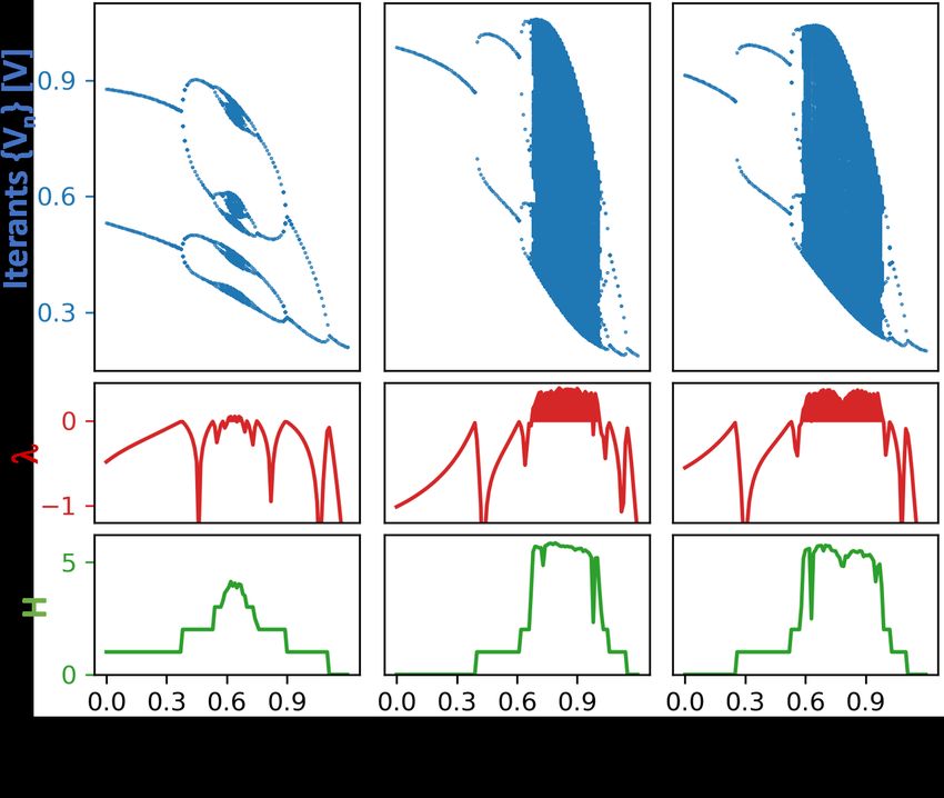
where f 0 is the derivative of the corresponding spline.
The Lyapunov exponent is a logarithmic measure of
the rate at which the sequence diverges, and a positive
Lyapunov exponent (λ > 0) guarantees chaos for one-
dimensional maps [21]. We use this to identify regions
of Vbias for which the system is chaotic.
4) An objective function based on the Lyapunov exponent
Oλ defined as maxα (λ) or λm is devised. The opti-
mization algorithms discussed in Secs. III-B and III-C
are used to satisfy this objective function and return a
set of widths and bias voltages such that the system is
chaotic.
A. Parameters Affecting Chaogate Operation Figure 2: (a) GA Flowchart with example showing (b) population
initialization; (c) selection of fit members from the population; (d)
As discussed in the previous section, the threshold voltage crossover between fit members to create new members; (e) mutation
of the transistors play a huge role in determining the behav- of genes in certain members; and (f) the new population.
ior of the circuit and thus the chaotic behavior. The other
parameter which we have not yet discussed but is equally B. Bayesian Optimization
important is the ratio (W/L). For an ideal N-type MOSFET Bayesian optimization [24] is a statistical approach for
or NMOS transistor (ignoring channel-length modulation), the finding the maximum of an objective function f that is costly
current through the transistor is given by [22] to evaluate over the full range of its argument(s) x ∈ X.
The technique is based upon Bayesian statistics, in which
0, VGS < VT H ,
conditional probability distributions are continuously updated
W
IDS = µ n Cox (VGS − VT H )VDS VDS < VDSAT , (4)
L
1 µn Cox W (VGS − VT H )2
VDS > VDSAT ,
as new data is acquired. In practice, Bayesian optimization
2 L
techniques amount to algorithms that sample the space X to
where µn is the electron mobility, Cox is the gate oxide maximize the conditional probability that a particular point
capacitance, VT H is the threshold voltage of the transistor, x∗ = argmaxx∈X [f (x)] is the location of the function
and VDSAT is the voltage level at which the current saturates. maximum, given all previous observations.
Similar expressions are available for PMOS transistors. From To this end, various sampling algorithms have been devised,
Eq. (4), we see that, for a specific voltage instance of VGS though the most common are Gaussian processes, which
(voltage across gate-source terminal of the transistor) and VDS draw samples assuming independence among the arguments.
(voltage across drain-source terminal of the transistor), IDS is Similarly, one may provide a prior probability distribution
directly proportional to (W/L). This then affects the transfer encoding the likelihood that the function maximum lies at each
characteristics of the circuit, which can dramatically affect the point in the space. The most common prior is a uniform prior,
chaotic behavior of the circuit as well. Thus, the transistor expressing an initial assumption that the function maximum is
sizes, specified by (W/L), must be chosen meticulously to equally likely to occur anywhere.
obtain the desired chaotic operation. We choose L to be the Here, we consider a uniform prior and a Gaussian process
minimum length allowed by the process technology node. The as the sampling algorithm of our Bayesian optimizer (BO).
widths W and Vbias are chosen using the optimization algo- Details on the parameter space, objective function, and imple-
rithms - Bayesian optimization (BO) and Genetic Algorithm mentation are given in Sec. IV.
(GA).
Brief comparison of the optimization algorithms: BO is C. Optimization using Genetic Algorithm
considered one of the most data-efficient frameworks for op- Genetic Algorithm (GA) is an evolutionary-based optimiza-
timization tasks, but it can be computationally expensive with tion technique inspired by Darwin’s theory of natural selection.
complexity O(n3 ) where n is the number of evaluations of The basic idea in GA is to find the fittest individual or the best
candidate solutions. GA, on the other hand, is data inefficient solution over a specific search space using three evolutionary
but computationally much less intensive than BO. The search operators - selection, crossover, and mutation - that are applied
heuristics used by evolutionary algorithms in GA take constant to a population of chromosomes as shown in Fig. 2a. Chro-
time for generating candidate solutions [23]. As such, one has mosomes are individuals that represent potential solutions to
clear advantage over the other depending on the task at hand. a problem (e.g., 1 through 4 represents different chromosomes
However, for tasks that fall in the middle of the two (i.e., in Fig. 2b). A chromosome is typically represented as a string
with a moderate evaluation cost), choosing one over the other of binary bits or real numbers called genes. During the start
becomes difficult. As the optimization problem that we deal of the algorithm, a large population of these chromosomes
with has not been thoroughly studied before, choosing between is created at random. Each chromosome is assigned a metric
BO and GA seems non-trivial. Therefore, we have applied both value based on the fitness function, which determines how
algorithms separately and presented the results. good the chromosome is at solving the problem. If it solves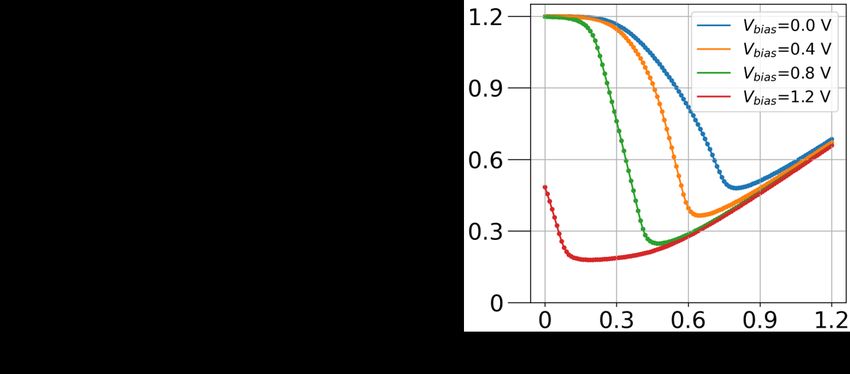
Figure 3: Simulation setup showing the procedure used to obtain a
chaotic set of widths.

the problem, then the algorithm halts. Otherwise, depending
on the fitness values, only a few chromosomes are selected          Figure 4: Cobweb diagram showing the first two iterations {Vn } =
as denoted by the step selection (see Fig. 2c). The next steps      {V0 , V1 , V2 } of the chaogate map Vn+1 = f (Vn ) starting at V0 = 0.2
                                                                    V for Vbias = 0.1 V.
involve creating new chromosomes, which is accomplished by
swapping genes of two fit chromosomes in a process called
crossover, as shown in Fig. 2d, and by mutating certain genes       of fixed values (Fig. 5a) while a filled region of non-repetitive
of the chromosomes in a process called mutation, as shown           values suggests chaos (Fig. 5b). This behavior of the system
in Fig. 2e. This concludes one run or generation of the GA          can also be examined using a bifurcation diagram (Fig. 5c)
algorithm and this evolution process continues until the fittest    which shows the values visited by the system as the bifurcation
chromosome is created or a stopping criterion is met [25].          parameter (Vbias in our case) changes. From Fig. 5c, we
In a particular GA, only a fraction of the chromosomes are          observe regions of chaos and windows of periodic behaviour
replaced, and the selection process is biased towards the fitter    of the chaogate circuit. Lastly, we use BO and GA to suggest
individuals.                                                        desirable W for chaogate design.
GA optimization for chaogate design: In the context of                 For each sequence {Vn }|α (Eq. (2), Fig. 4), we find that
chaogate design, our fitness function is the Lyapunov exponent      N = 2, 500 with T = 500 is enough to obtain representative
(Eq. (3)) and the fittest chromosome is the one with the highest    sequences starting with an arbitrarily chosen V0 = 0.45 V.
Lyapunov exponent. For this analysis, a stopping criteria can       We fix these quantities for the remainder of this simulation.
be provided such as λ = k, where k is a positive real number,       Next, we calculate the Lyapunov exponent using Eq. (3).
or the algorithm is allowed to run for fixed number of iterations   We use λ > 0 to identify regions of Vbias for different W
or generations after which the values of W with the maximum         such that the system is chaotic (Fig. 5, 6). Similarly, we
λ are selected for the chaogate.                                    calculate the Shannon entropy (H) of the long-term behavior
                                                                    of the probability density function of each chaogate iteration
         IV. S IMULATION R ESULTS AND A NALYSIS                     sequence using
A. Simulation Setup                                                                           n=N
                                                                                               X+T
                                                                                H(α) = −               pn (α) log2 (pn (α)),           (5)
   We simulate the netlist shown in Fig. 1a in multiple com-
                                                                                                n=T
mercial technology nodes with 65 nm assumed when not
specified. A DC sweep of Vout versus Vin with Vbias ∈               where pn (α) is the frequency of observation of element Vn
[0, 1.2] V and VDD =1.2 V is performed to obtain the transfer       from the iterated map sequence {Vn }|α .
characteristics like those in Fig. 1b. As discussed earlier,
                                                                    C. Optimization Results and Analysis
we optimize W . The creation of netlist, the optimization
of transistor parameters, and the corresponding simulations            As discussed in Sec. III, the optimization cost corresponding
(with new width values) are entirely done within the Python         to the design of the chaogate has not been determined previ-
environment as shown in Fig. 3. We use PySPICE [26] v.              ously. Here, we consider both data- and time-efficient types,
1.4.3, which is an open-source module that allows the user          namely, BO and GA to optimize the function Oλ = maxα (λ),
to simulate and manipulate SPICE netlists within Python by          which explores the width space to return a specific set W .
interfacing to the Ngspice v. 33 simulator.                         To allow a fair comparison, the same number of iterations
                                                                    is considered for the BO and GA. Moreover, the range of
B. Simulation Procedure                                             parameters searched to perform the optimization is also fixed.
   In the simulations, we use the procedures discussed in           Specifically, for the BO, we use the Python package skopt
Sec. III for generating f (V ). At intermediate steps, a conve-     and the function gp mimimize with default parameters. For
nient method for visualizing the dynamics is through a cobweb       GA, we devise a simple evolutionary algorithm as described
diagram [21], which overlays the trajectories on the transfer       in Sec. III-C.
function with an example shown in Fig. 4. We iterate the map        Results with objective of λm : We run the BO and the GA
to produce a cobweb diagram that describes the behavior of          algorithms for 100 generations and the corresponding results
the system - a closed polygon indicates a repetitive sequence       are shown in Figs. 6b and 6c. We also compare these results
Figure 5: Cobweb plots of two regions showing (a) non-chaotic and
(b) chaotic system behavior as Vbias is changed for fixed W = Figure 7: Dynamics of chaogate with the maximum entropy (a)
(120, 120, 2000) nm. (c) Bifurcation diagram, which shows the set Hm = 6.18 bits at W = (331, 65, 950) nm obtained using BO.
of unique chaogate iteration points {Vn } on the vertical for each bias Note the two bands of chaotic behavior, one of which indicates
voltage on the horizontal. chaos even at Vbias = 0. Both regions are punctuated by periodicity
characterized by drops in H and λ. (b) Hm = 5.89 bits at
W = (1320, 87, 2060) nm obtained using GA.
parameters searched by the BO and GA, the GA converges
to a result, where the λ’s are positive over a wider range. In
comparison to the chaotic system described in Ref. [15], the
optimization algorithms clearly find circuits that show larger
range of chaos over Vbias . As shown in Fig. 6a, this system
has a very narrow chaotic region (the shaded red region) at
around Vbias = 0.6 V. The wider chaotic region can also prove
to be effective against process variation and noise, which will
be the subject of our future work.
Results with objective of Hm : Now, if we change our objec-
tive from λm to the maximum value of the entropy Hm , the
structure and position of the chaotic regions shift, giving us the
result as shown in Fig. 7. The chaogate designer can certainly
choose to have both λ and H maximized by providing a multi-
objective function (λm , Hm ) to the optimization algorithms.
The maximum-entropy region shown in both Figs. 7a and 7b
Figure 6: Dynamics of the chaogate (a) for W = demonstrates a broad band of chaos at low bias voltages
(480, 480, 4800) nm and L = 60 nm over the full range of specifically Fig. 7a which is chaotic even at 0 V. This may be
Vbias [15]. (Blue) Bifurcation diagram showing set of map iterations desirable for extremely low power cryptographic primitives.
{Vn }. (Red) Lyapunov exponent; shaded red regions are where However, there exist small bands of periodicity in this region,
λ > 0 and the system is chaotic. (Green) Entropy of the map
which may interrupt cryptography.
iterations in bits, calculated by binning {Vn } in 0.01 V increments.
(b) with λm = 0.40 at W = (65, 247, 958) nm obtained using BO. In contrast, optimizing for λ, as shown in Figs. 6b and 6c,
(c) with λm = 0.37 at W = (66, 177, 2052) nm obtained using demonstrates the highest density chaotic region of the three
GA. (the red shaded region is larger compared to Fig. 6a). The
set of states here may have applications in primitives prior-
itizing cryptography at the expense of power consumption.
with the state-of-the-art chaogate circuit specified in Ref. [15] Additionally, the chaogates in these regions may have near
and shown in Fig. 6a. Both optimization algorithms are run maximal entropy. The 0.01 V bin space provides a total of
to obtain a set of widths that achieve the largest Lyapunov log2 (120) = 6.91 bits for our estimate. We see in each plot
exponent λm . The results obtained from these optimization that Hm ∼ 6 bits, naı̈vely suggesting an entropy density
algorithms look similar in that the change in H (the green around 6/6.91 ≈ 90%. More advanced entropy measures, such
steps) and the sign of λ (blue spikes) at each bifurcation are as the Kolmogorov-Sinai entropy, may yield more accurate
approaching the maximal density chaotic region around 0.8 V. results by taking into account information revealed by the
Nevertheless, for the same number of iterations and range of ordering of {Vn }. This is the subject of future work.TABLE I: Comparison of width values W = (W1 , W2 , W3 )
Chaos: An Interdisciplinary J. of Nonlinear Science, vol. 20, no. 3,
obtained for different technology nodes, namely a commercial 65 nm p. 037107, 2010.
and PTM 45 nm, 90 nm, and 130 nm. The widths are optimized to [2] S. Sinha and W. L. Ditto, “Dynamics based computation,” Phys. Rev.
obtain maximum Lyapunov exponent using Bayesian Optimization Lett., vol. 81, no. 10, p. 2156, 1998.
(BO) and Genetic Algorithm (GA). The resulting Hm is also reported. [3] T. Munakata, S. Sinha, and W. L. Ditto, “Chaos computing: imple-
mentation of fundamental logical gates by chaotic elements,” Trans. on
BO GA Circuits and Systems I: Fundamental Theory and Applications, vol. 49,
no. 11, pp. 1629–1633, 2002.
Node W W
λm Hm λm Hm [4] S. Sinha and W. L. Ditto, “Computing with distributed chaos,” Phys.
[nm] [nm] [nm]
Rev. E, vol. 60, no. 1, p. 363, 1999.
45 (86, 47, 992) 0.48 5.39 (132, 67, 1983) 0.5 5.53 [5] G. S. Rose, “A chaos-based arithmetic logic unit and implications for
65 (65, 247, 958) 0.4 5.37 (66, 177, 2052) 0.37 5.41 obfuscation,” in Computer Society Annual Symp. on VLSI, pp. 54–58,
IEEE, 2014.
90 (162, 149, 2032) 0.35 5.96 (114, 99, 2035) 0.35 5.93 [6] B. Kia, J. F. Lindner, and W. L. Ditto, “A simple nonlinear circuit
130 (201, 236, 1882) 0.38 6.03 (207, 138, 2045) 0.34 6.05 contains an infinite number of functions,” Trans. on Circuits and Systems
II: Express Briefs, vol. 63, no. 10, pp. 944–948, 2016.
[7] L. Keuninckx, G. Van der Sande, and J. Danckaert, “Simple two-
D. Demonstration on Different Technology Nodes transistor single-supply resistor–capacitor chaotic oscillator,” Trans. on
Circuits and Systems II: Express Briefs, vol. 62, no. 9, pp. 891–895,
Our optimization approach is flexible and can be applied 2015.
to other technology nodes, chaotic circuits, and other analog [8] A. Namajunas and A. Tamasevicius, “Modified Wien-bridge oscillator
circuits. Here, we use it to port chaotic behavior of the for chaos,” Electronics Lett., vol. 31, no. 5, pp. 335–336, 1995.
[9] P. S. Linsay, “Period doubling and chaotic behavior in a driven anhar-
chaogate to different technology nodes, thus relieving the monic oscillator,” Phys. Rev. Lett., vol. 47, no. 19, p. 1349, 1981.
designer’s burden. As seen in Table I, the optimizer returns [10] J. R. Piper and J. C. Sprott, “Simple autonomous chaotic circuits,” Trans.
a set of widths for different transistor technologies and it can on Circuits and Systems II: Express Briefs, vol. 57, no. 9, pp. 730–734,
2010.
be optimized to obtain either λm or Hm . [11] L. Keuninckx, M. C. Soriano, I. Fischer, C. R. Mirasso, R. M. Nguimdo,
The key message that the results in Table I convey is and G. Van der Sande, “Encryption key distribution via chaos synchro-
that both the BO and GA could converge to (almost) similar nization,” Scientific Reports, vol. 7, p. 43428, 2017.
[12] I. Mishkovski and L. Kocarev, ”Chaos-Based Public-Key Cryptogra-
widths regardless of the transistors technology. Nevertheless, phy”, pp. 27–65. Berlin, Heidelberg: Springer Berlin Heidelberg, 2011.
to decide which algorithm should be chosen to perform the [13] T. Stojanovski, J. Pihl, and L. Kocarev, “Chaos-based random number
optimization task, time complexity can play a crucial role. To generators. Part II: practical realization,” Trans. on Circuits and Systems
I: Fundamental Theory and Applications, vol. 48, no. 3, pp. 382–385,
address this, we measure the time that the algorithms take 2001.
to optimize the circuit 100 times for the commercial 65 nm [14] J. Bohl, L.-K. Yan, and G. S. Rose, “A two-dimensional chaotic logic
model. The BO takes 157.3 s, while the GO finishes the gate for improved computer security,” in 58th Intrl. Midwest Symp. on
Circuits and Systems, pp. 1–4, IEEE, 2015.
task in 143.7 s. Similar trends have been observed for other [15] M. B. Majumder, M. S. Hasan, M. Uddin, and G. S. Rose, “Chaos
transistor models. Note that although the difference between computing for mitigating side channel attack,” in Intrl. Symp. on
the time complexity of the BO and GA is not substantial in Hardware Oriented Security and Trust, pp. 143–146, IEEE, 2018.
[16] M. B. Majumder, M. S. Hasan, A. Shanta, M. Uddin, and G. Rose,
our scenario, this difference can affect the efficiency of the “Design for Eliminating Operation Specific Power Signatures from
design process for larger or more complex analog circuits. Digital Logic,” in Proc. of the Great Lakes Symp. on VLSI, p. 111–116,
ACM, 2019.
V. C ONCLUSION AND F UTURE W ORK [17] M. M. Alam, S. Chowdhury, B. Park, D. Munzer, N. Maghari, M. Tehra-
nipoor, and D. Forte, “Challenges and opportunities in analog and mixed
AI is a promising approach for co-optimization of circuit signal (ams) integrated circuit (ic) security,” J. of Hardware and Systems
security and performance. Here, we present a clear framework Security, vol. 2, no. 1, pp. 15–32, 2018.
for designing chaotic circuits and explore the optimization [18] M. Fakhfakh, Y. Cooren, A. Sallem, M. Loulou, and P. Siarry, “Analog
circuit design optimization through the particle swarm optimization
problem underlying such a task in terms of its computational technique,” Analog Integrated Circuits and Signal Processing, vol. 63,
cost. As this cost has not been discussed in the literature, we no. 1, pp. 71–82, 2010.
have applied two well-known optimization methods, namely [19] M. Taherzadeh-Sani, R. Lotfi, H. Zare-Hoseini, and O. Shoaei, “Design
optimization of analog integrated circuits using simulation-based genetic
BO and GA borrowed from AI, which are less time-efficient algorithm,” in Intl. Symp. on Signals, Circuits and Systems, vol. 1,
and less data-efficient, respectively. In the current literature, pp. 73–76, IEEE, 2003.
it has been suggested to combine the two [23], which will [20] P. Dudek and V. Juncu, “Compact discrete-time chaos generator circuit,”
Electronics Lett., vol. 39, no. 20, pp. 1431–1432, 2003.
be a subject of our future work. Moreover, future work in- [21] H. G. Schuster and W. Just, Deterministic chaos: an introduction. John
cludes tuning the hyperparameters of the optimization routine, Wiley & Sons, 2006.
testing other objective functions and constraints (including [22] T. Sakurai and A. R. Newton, “A simple MOSFET model for circuit
analysis,” IEEE transactions on Electron Devices, vol. 38, no. 4,
traditional circuit metrics such as area and power), performing pp. 887–894, 1991.
a noise sensitivity analysis, and completely exploring the [23] G. Lan, J. M. Tomczak, D. M. Roijers, and A. Eiben, “Time Efficiency in
transistor-width parameter space to identify different trends. Optimization with a Bayesian-Evolutionary Algorithm,” arXiv preprint
arXiv:2005.04166, 2020.
Additionally, the results obtained here will be used to fabricate [24] P. I. Frazier, “A tutorial on Bayesian optimization,” arXiv preprint
chaogates in silicon for further experimental research. arXiv:1807.02811, 2018.
[25] R. Y. Acharya, S. Chowdhury, F. Ganji, and D. Forte, “Attack of the
R EFERENCES Genes: Finding Keys and Parameters of Locked Analog ICs Using
Genetic Algorithm,” in Intrl. Symp. on Hardware Oriented Security and
[1] W. L. Ditto, A. Miliotis, K. Murali, S. Sinha, and M. L. Spano, Trust, pp. 284–294, IEEE, 2020.
“Chaogates: Morphing logic gates that exploit dynamical patterns,” [26] F. Salvaire, “PySpice.” https://pyspice.fabrice-salvaire.fr, 2020.You can also read