A NEW CMY CAMERA TECHNOLOGY USING AL-TIO2-AL NANOROD FILTER MOSAIC INTEGRATED ON A CMOS IMAGE SENSOR
←
→
Page content transcription
If your browser does not render page correctly, please read the page content below
A new CMY camera technology using Al-TiO2-Al nanorod filter
                                                           mosaic integrated on a CMOS image sensor
                                                            X. He1 , Y. Liu1 , P. Beckett2 , H. Uddin3 , A. Nirmalathas1 , and R. R. Unnithan1
                                                       1
                                                           Department of Electrical and Electronic Engineering, The University of Melbourne,
                                                                                    Melbourne, VIC, 3010, Australia.
                                                              2
                                                                School of Engineering, RMIT University, Melbourne, VIC, 3000, Australia.
                                                           3
                                                             Melbourne Centre for Nanofabrication, Australian National Fabrication Facility,
arXiv:2010.11680v1 [physics.ins-det] 16 Oct 2020

                                                                                     Clayton, VIC, 3168, Australia.

                                                                                                    October 23, 2020

                                                           Corresponding author: R. R. Unnithan (e-mail: r.ranjith@unimelb.edu.au)

                                                                                                          Abstract
                                                                  A CMY colour camera differs from its RGB counterpart in that it employs a subtractive colour
                                                             space of cyan, magenta and yellow. CMY cameras tend to performs better than RGB cameras in
                                                             low light conditions due to their much higher transmittance. However, conventional CMY colour
                                                             filter technology made of pigments and dyes are limited in performance for the next generation image
                                                             sensors with submicron pixel sizes. These conventional filters are difficult to fabricate at nanoscale
                                                             dimensions as they use their absorption properties to subtract colours. This paper presents a CMOS
                                                             compatible nanoscale thick CMY colour mosaic made of Al-TiO2 -Al nanorods forming an array
                                                             0.82 million colour pixels of 4.4 micron each, arranged in a CMYM pattern. The colour mosaic
                                                             was then integrated onto a MT9P031 monochrome image sensor to make a CMY camera and the
                                                             colour imaging demonstrated using a 12 colour Macbeth chart. The developed technology will have
                                                             applications in astronomy, low exposure time imaging in biology and photography.
                                                                  Keywords: CMY image sensor, Plasmonics, nanophotonics

                                                   1         Introduction
                                                   In a conventional CMOS based image sensor, colour imaging relies on the integration of filters on top of
                                                   the photodetector array. These filters typically cover the three primary colours (bands): red (around 650
                                                   nm), green (550 nm) and blue (450 nm) (RGB), predominately in a Bayer pattern [1-9]. As the human
                                                   eye is more sensitive to green light than either red or blue, the widely used Bayer filter mosaic is formed
                                                   with twice as many green as red or blue filters. RGB colour space uses an additive colour mixing of red,
                                                   green, and blue that combine to create a white output.
                                                        In contrast, CMY (cyan, magenta, and yellow) is a subtractive colour mixing scheme where colour
                                                   filters are used to remove certain wavelengths of white light. For example, cyan is obtained when the red
                                                   is subtracted from the image. Similarly, magenta and yellow are obtained by subtracting the green and
                                                   blue respectively. In RGB space, a red filter transmits only about 1/3 of the visible light as the remaining
                                                   light is absorbed in the filter (only the red light passes through the filter). In contrast, the corresponding
                                                   cyan filter in CMY colour space transmits about 2/3 of the spectrum because only the red is subtracted,
                                                   and the remaining is transmitted through the filter. In general, CMY colour filters pass approximately
                                                   twice the spectral power as their corresponding RGB filters [11] and so are promising candidates for
                                                   low-light imaging applications. Examples of such applications include astronomical imaging of nebula
                                                   and the like that are characterized by dim objects against a dark background. Furthermore, astronomical
                                                   images are often required to be captured with short exposure times, lest rotation effects blur the image
                                                   (for example, images of Jupiter). These requirements are best served by high transmission filter schemes
                                                   such as CMY.
                                                        Conventional CMY colour filters are based on the absorption properties of organic dye-based materials
                                                   or pigments to subtract selected wavelengths from the incident light. However, as the pixel size in the

                                                                                                               1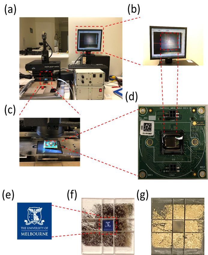
sensor is reduced to submicron dimensions [8], conventional CMY colour filters start to suffer from
colour cross talk as their performance deteriorates at nanoscale thicknesses [1-9]. Further, existing CMY
technology must be fabricated in several steps, which presents severe challenges when trying to accomplish
submicron-scale alignment. These issues demand the development of new CMY color filter technologies
that can be fabricated easily at nanoscale thickness, using CMOS compatible materials, and that will
support the creation of millions of filter pixels within a colour mosaic.
     Colour filters based on plasmonic effects [1-9, 11-27] are suitable candidates due to their ability to
be precisely tuned using nanoscale thick films. Colour filters based on localized surface plasmons are
superior to those based on surface plasmons as the former are angle independent. As a result, the
transmitted colours in LSP based filters are same for any angle of incidence, an important requirement
for image sensor applications. Recently, gold (Au) nano-disk based CMY filters have been demonstrated
with useful characteristics such as polarization independence and angle insensitivity [14]. However, Au
based plasmonic filters are limited in their colour tuning capability, especially below 550 nm as Au does
not readily support plasmonic resonance peaks below that wavelength [28].
     CMY filters with high transmission coefficients have been reported based on silver (Ag) nano-slits
[15], nano-disk [17] and Si meta-surfaces [18-19]. However, Ag oxidizes quickly in air and this degrades
the optical properties, thereby mandating additional protective coatings that can further affect the filter
characteristics. CMY filters operating in reflection mode based on surface plasmon polaritons (SPP) are
demonstrated in [21-24], but the reflection mode is not suitable for image sensor applications.
     In this paper, we present a colour filter mosaic built from a hexagonal array of Al-TiO2 -Al nanorods
on a quartz substrate that is derived from a subtractive MDM (metal-dielectric-metal) nanohole array
structure. The structure exhibits a high transmission efficiency and narrow bandwidth to produce supe-
rior colour separation. Colour tuning is achieved by varying the rod radius across the array, while keeping
the base thickness constant, thereby forming a mosaic of CMY filters across the substrate. Further, we
have applied this colour mosaic to develop a CMY camera. The 4mm x 4mm optical filter mosaic en-
compasses 0.82 million pixels, each pixel being 4.4 µm square and arranged in CMYM pattern. The
filter has been integrated onto a monochrome image sensor (MT9P031) to create a CMY camera and its
imaging capabilities demonstrated using a standard 12 colour Macbeth chart. To date, there has been
no prior demonstration of a full camera system using a nanoscale thick CMY mosaic integrated onto an
image sensor that illustrates its feasibility for imaging applications. This is the first such demonstration.

2     Results
2.1    Filter Design and Fabrication
Fig. 1a shows the proposed structure of the CMY colour filter, which is formed from Al-TiO2 -Al nanorods
fabricated on a quartz substrate and then embedded in a SOG (spin on glass [33]) matrix for refractive
index matching. The optical characteristics of this structure can be considered to arise from a Fano
resonance in which the top and bottom metal disk operate together as a coupled dipole, enhancing
the magnetic field between them to produce both destructive and constructive (i.e., in-phase and anti-
phase) interference modes. Choosing an appropriate radius and period for the structures results in a
narrow reflection peak and a deep transmission valley that are sensitive to the symmetry of the dipole
elements [32]. It has been shown in previous work related to nanodisks [27, 32] that these structures
exhibit a broad (in-phase) resonance at smaller wavelengths and a narrow anti-phase resonance at larger
wavelengths. This can be described in terms of a Q factor, which is proportional to the ratio of the
resonant frequency to the FWHM. It is also clear that, while introducing asymmetries can strengthen
the peaks (in particular, the anti-phase resonance), it introduces an undesirable sensitivity to the angle
of incidence [32]. As a result, our work has kept the thickness and radius of both the top and bottom
metal disks the same, which has the added advantage of simplifying its fabrication.
    The CMY filters were computationally investigated in 3D using finite element methods (FEM) im-
plemented in COMSOL MULTIPHYSICS. The simulation model consists of a unit cell on a semi-infinite
thick quartz substrate consisting of a single nanorod at the centre and one-quarter of a nanorod at each
corner as shown in Fig. 1a (red rectangle). Each rod consists of an Al-TiO2 -Al stack with thickness of 40
nm, 90 nm and 40 nm, respectively. The simulated unit cell on the semi-infinite glass substrate is covered
with spin on glass. The 3D simulation geometry has been truncated using perfect matched layer (PML)
and periodic boundary condition (PBC). The PML is applied on the top and at the bottom, PBCs are
applied on the four sides of the cell as highlighted in the red block of Fig. 1a. For calculating the peak
wavelengths, the refractive index of glass is set to 1.5, spin on glass 1.45 and the wavelength dependent

                                                     2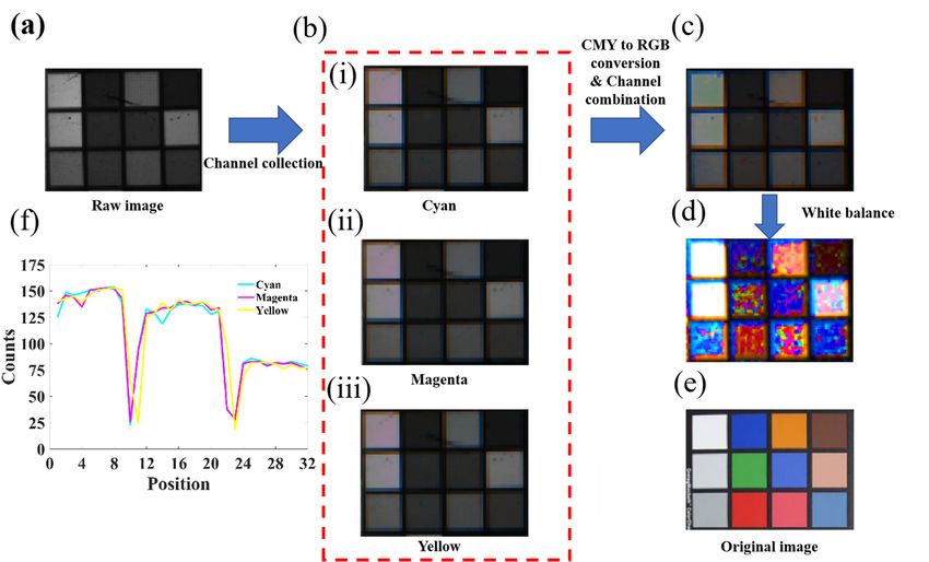
Figure 1: Simulation results of Al-TiO2 -Al nanorod based CMY (cyan, magenta, yellow) filter mosaic:
(a) Al-TiO2 -Al nanorods in hexagonal array on a quartz substrate covered with spin-on-glass, (b) The
normalized electric field at valley wavelength for the filters: yellow (470 nm), magenta (570 nm) and
cyan (670 nm). Electric field at 470 nm, (c) The normalized electric field of cross section (red dotted
line) at valley wavelength for the filters, (d) Numerically simulated transmission spectra of the CMY
colour filters. The wavelength is swept from 300 nm to 800 nm (e) CIE chart of simulated CMY colours
in the filter mosaic.

          Table 1: Parameters of Al-TiO2 -Al Nanorod (layer thickness, period, rod diameter)
                       Parameters                  Cyan Magenta Yellow
                       Top Al thickness (nm)        40         40        40
                       TiO2 thickness (nm)          90         90        90
                       Bottom Al thickness (nm)     40         40        40
                       Period (nm)                  500       430        350
                       Diameter (nm)                60         90         40

refractive index of Al was taken from Rakic’s data [34]. The refractive index of TiO2 (i.e., 2.1) was
obtained experimentally by measuring values from a TiO2 film deposited with an E-beam evaporator.
This value was also used in the simulation model. The transmission coefficient has been obtained from
S-parameters using the port boundary conditions.
    The wavelength of light was swept from 300 nm to 800 nm to find the valley transmission [35], keeping
the thickness values constant while varying the rod radius from 20 nm to 30 nm. The normalised electric
field of each colour filter-yellow (470 nm), magenta (570 nm) and cyan (670 nm)—at their resonant
wavelength (i.e., the valley wavelength) is shown in Figure 1b. The corresponding normalized electric
field across each CMY pillar is shown Fig. 1c while Fig. 1d shows the simulated transmission spectrum
for CMY filters. The layer parameters (thickness, period and rod diameter) are summarised in Table
1. Fig. 1e plots the simulated CMY filter wavelengths on the CIE chromaticity chart, illustrating that
these fall in an appropriate part of the colour space, thereby demonstrating their suitability for imaging
applications.
    As the refractive index of the middle (insulator) layer has substantial influence on the optical prop-
erties of the filter, we also investigated a number of alternative dielectric materials for this layer. In
our simulation model, we applied SiO2 , TiO2 , Si (assuming an ion assisted deposition with E-beam
evaporator) and Ge with refractive index values of 1.45, 2.1, 2.8 and 4, respectively. These materials
were used to simulate a cyan colour filter and the results are summarised in Figure 2. Note that these
data are measured using ellipsometry (J.A. Woollam M-2000DI). As shown in Fig. 2, the transmission
spectrum exhibits the largest transmission contrast and smallest linewidth (to produce a more vivid cyan

                                                    3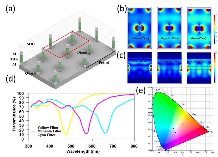
Figure 2: Comparison of transmission spectra from Al-X-Al, where X represents the middle dielectric
material: SiO2 , TiO2 , Si and Ge.

     Figure 3: Strategy for fabricating the Al-TiO2 -Al nanorod based CMY colour filter mosaic.

colour) with TiO2 compared to SiO2 , Si and Ge so this material was selected for the remainder of our
experiments.
    We fabricated a 4 mm x 4 mm mosaic onto a quartz substrate using standard nanofabrication tech-
niques [36-39]. The mosaic comprises repeating CMYM units in both the horizontal and vertical di-
rections to form a colour array. The fabrication strategy using a PMMA-MMA bilayer is described as
follows (see Fig. 3).
    Firstly, a 1 mm thick quartz substrate was cleaned with acetone under sonication for 5 minutes
followed by IPA and DI water rinse. The substrate was then preheated at 80°C for 10 minutes and a thin
EL9 (MMA) layer spin-coated onto the quartz at 3000 RPM for 1.5 minutes and baked at 180°for 15
minutes. A thin PMMA A2 layer was spin-coated onto the sample at 3000 RPM for 1.5 minutes and baked
at 180°C for 5 minutes. To ameliorate problems with charging of the quartz substrate under Electron
Beam Lithography (EBL), a 30 nm Cr layer was deposited on the sample by conformal sputtering to
finish the sample preparation.
    After patterning with EBL (Vistec EBPG5000plusES), the Cr layer was removed using 1 minute in a
Cr etchant, stopped by 5% H2 SO4 . The sample was then developed with diluted MIBK (MIBK:IPA=1:3)
for 1 minute and stopped by IPA and DI water. It can be seen in Fig. 3 that the MMA exhibits a bowl
shape after development, which makes subsequent lift off easier due to the smaller contact area between
the Al-TiO2 -Al nanorod and the quartz.
    Finally, the Al-TiO2 -Al nanorod was deposited by E-beam evaporator (Intlvac Nanochrome II). The
deposition rate for the TiO2 was 0.1 nm/s. After MMA/PMMA lift-off, the filter was completed by

                                                  4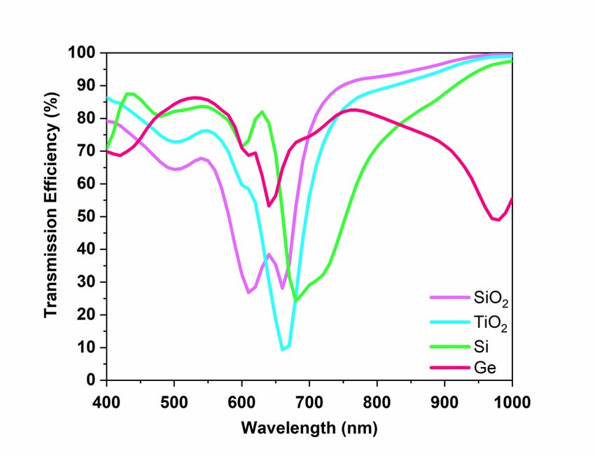
Table 2: Optical Characteristics of the CMY Filter Mosaic
Cyan Magenta Yellow
Transmission Characteristic Sim Expt Sim Expt Sim Expt
Valley Wavelength (nm) 660 670 580 580 470 480
Maximum Contrast (%) 60 45 70 47 80 50
Maximum Efficiency (%) 90 90 100 92 100 90
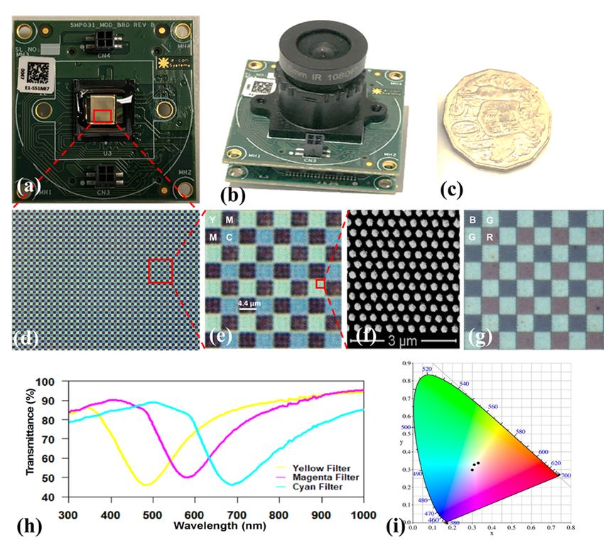
Figure 4: Integration of the CMY colour mosaic on the image sensor. (a) CMOS image sensor, MT9P031
integrated with 4 mm x 4 mm CMY colour mosaic using flip chip bonder for alignment; (b) CMY camera
developed with optics (f number 1.4) for imaging; (c) an Australian 50c coin as a reference to show the
size of the CMY camera; (d) the CMY colour mosaic under optical microscope; (d) magnification ×20
(e) magnification ×40; (f) SEM image of the filter mosaic made of Al-TiO2 -Al nanorods from top view
(cyan is shown); (g) Reflected RGB colours from (e); (h) Experimental transmission spectra of the CMY
color filters from the color mosaic; (i) CIE chromaticity chart of the CMY filters in the mosaic from
experimental data.
spin-coating with SOG (Desert NDG-2000) at 2000 RPM for 20 seconds and baking at 210°C for 15
minutes.
Fig. 4d shows an image of the CMYM mosaic in transmission mode under an optical microscope
(Olympus BX53M) with 20× magnification and an enlarged section of this is shown in Fig. 4e. A
SEM image of part of a cyan pixel (top view) is shown in Fig. 4f. Note that, as the sample surface is
non-conductive, 7nm of Cr was deposited prior to performing the SEM imaging, which altered the shape
of the nanorods. Finally, it can be seen from the reflection mode image (Fig. 4g) that the reflected light
from the sample (i.e., Fig. 4e) is RGB.
The transmission spectrum of the fabricated mosaic was measured using a CRAIC spectrometer
(Apollo Raman Microspectrometer). It can be seen from Fig. 4h that the maximum transmittance of
the individual Cyan, Magenta and Yellow cells is around 90%. The spectrum displays high transmission
without any secondary resonances from UV to Near-IR wavelengths. Figure 4i positions these exper-
imentally measured CMY data on the standard CIE chromaticity chart. The detailed results for the
CMY filter are collated in Table II.
As is evident from Table 2, generally good agreement was observed between the simulated and exper-
imental data in the case of the valley wavelength and efficiency values. However, the peak transmission
contrast is consistently smaller (by almost 40% for yellow). This difference may be caused by the surface
5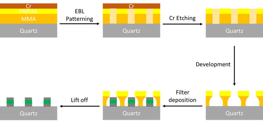
Figure 5: Integration of CMY filter mosaic on the CMOS image sensor MT9P031: (a) flip chip bonder,
(b) display showing the alignment of filter colour pixels on the sensor pixels, (c) placement of the filter
mosaic on the sensor (d) CMY filter aligned on the image sensor after being glued by PMMA powder
diluted with anisole, (e) logo of the University of Melbourne (f) CMY filter with the logo behind it to
show its high transmission efficiency, (g) CMY colour filter after being diced.

roughness of the deposited TiO2 . It has been observed in prior work [27] that defects and surface rough-
ness in the metal film can result in inhomogeneous broadening of the resonances without affecting the
FWHM and can even eliminate the anti-phase mode entirely. In order to achieve a relatively uniform
metal oxide layer, and therefore a high refractive index, the deposition rate of the E-beam evaporator
needs to be set as high as possible. This resulted in a surface roughness of around 3-5 nm in our work
(measured by Atomic Force Microscopy). In the absence of an additional planarization step, the top
Al disk becomes similarly rough, potentially affecting its behavior. However, this reduction in contrast
may be offset in part by the high transmission efficiency, which increases the received brightness. The
contrast can also be corrected by subsequent image processing.

2.2    Filter integration and Image Reconstruction
The CMYM mosaic was integrated onto a commercial CMOS sensor using a flip-chip bonder (Fineplacer
@Lambda) and raw images captured for further analysis as shown in Fig. 5. The CMOS image sensor
used in this experiment was a MT9P031 monochrome array with a pixel size of 2.2 µm. Fig. 5(a-d)
shows the CMY mosaic aligned and glued onto the image sensor. The glue was made in-house using
PMMA powder diluted with anisole solution and the filter was pressed onto the image sensor with just
sufficient force to exclude most of the air between them. The high transmission efficiency of the CMY
filter is demonstrated using the University logo on white paper which can be clearly seen through filter
(Fig. 5(e-g)). The overall filter mosaic size is 4 mm x 4 mm and each colour cell covers a 2 x 2 patch to
increase the light absorption and decrease the spatial crosstalk. Therefore, the pixel size in this mosaic
is 4.4 µm square. The image sensor integrated with the mosaic is then fitted with optics (f number =

                                                    6
Figure 6: Demonstration of colour imaging by the CMY camera: (a) 12-bit raw image of the 12 colour
Macbeth chart captured by CMY camera. (b) Three bands (cyan, magenta and yellow) extracted from
the raw image. (c) The three bands (three channel combination) are recombined to get a CMY color
image. (d) The CMY colour image is converted into RGB and applied color correction and white balance.
(e) Standard image of the 12 colour Macbeth color chart. (f) The plot shows signals from three pixel
numbers along the vertical red dotted line in the raw image.
1.4) for imaging as shown in Fig. 4b. The compact size of the CMY camera is shown by reference to an
Australian 50c coin1 (Fig. 4c).
The CMY camera was then used in an example imaging application shown in Fig. 6. Firstly, a raw
image of the standard 12-colour Macbeth chart (Figure 6e) was taken with the CMY camera (Fig. 6a).
The recorded 12-bit raw image data was then transmitted to a laptop for processing using MATLAB.
The raw data was first analyzed for saturation and signal intensity variation. Fig. 6f shows a plot of
the signals from the 12-colour Macbeth chart pixels across the transect indicated by the red dashed line.
The results show that the intensity variations are present in the raw image. Then, the individual CMY
pixel data were grouped to form separate images for each of cyan, magenta and yellow pixels (Fig. 6b).
Fig. 6c shows the reconstructed colour image. Next, a CMY to RGB conversion algorithm: R=Y+M-C;
G=Y+C-M; B=C+Y-M [10], was applied to transform the CMY image to RGB for display. Lastly,
colour correction and white balance were applied to recover the Macbeth chart as shown in Fig. 6e.
These results demonstrate that colours can be retrieved from the 12-bit raw image data and illustrate
correct operation of the CMY camera.
3 Conclusion
In conclusion, a CMY camera is demonstrated using a nanoscale CMY colour filter mosaic made of CMOS
compatible Al-TiO2 -Al nanorods with high transmission. The overall filter mosaic is 4 mm x 4 mm with
each pixel occupying 4.4 µm square in a CMYM pattern and is integrated onto a MT9P031 CMOS image
sensor using flip-chip bonding and an in-house prepared glue. The performance of the filter mosaic itself
was first characterised and then the correct operation of the integrated CMY camera was illustrated using
a 12 colour Macbeth chart as an object. The colours were retrieved using image processing algorithms.
The use of more powerful image processing algorithms (as employed by commercial camera systems)
will further improve the colour performance. This nanorod technology will overcome the limitations
imposed by conventional colour filter technology for creating CMY colour image sensors and cameras
with submicron pixel sizes. As a result, this technology is likely have applications ranging over astronomy,
low exposure time imaging in biology and general photography.
1A 12 sided coin measuring 31.65 millimetres between flat sides.
7Conflict of Interest
The authors declare that they have no conflict of interest.
Acknowledgment
This work was performed in part at the Melbourne Centre for Nanofabrication (MCN) in the Victorian
Node of the Australian National Fabrication Facility (ANFF). The authors acknowledge financial support
through ARC Discovery Project: DP170100363.
Author Contributions
X. H. and R. R. U conceived the idea. X. H carried out theoretical design, fabricated the CMY mosaic
filter and the optical measurements. X. H. Y. L performed the integration of the mosaic filter with
image sensor. X. H. Y. L. and P. B. processed the image data and analyzed the results. X. H and R.R.U
wrote the paper. R. R. U, H.U and A.N supervised the project. All authors discussed the results and
commented on the manuscript.
References
[1] S. Yokogawa, S. P. Burgos, H. A. Atwater, “Plasmonic Color Filters for CMOS Image Sensor
Applications,” Nano Letters, 12, 8, 4349-4354, 2012.
[2] S. P. Burgos, S. Yokogawa, H. A. Atwater, “Color Imaging via Nearest Neighbor Hole Coupling
in Plasmonic Color Filters Integrated onto a Complementary Metal-Oxide Semiconductor Image
Sensor,” Nano letter, 7, 11, 10038-10047, 2013.
[3] X. He, Y. Liu, K. Ganesan, A. Ahnood, P. Beckett, F. Eftekhari, D. Smith, Md H. Uddin, E.
Skafidas, A. Nirmalathas, R. R. Unnithan, “A single sensor based multispectral imaging camera
using a narrow spectral band color mosaic integrated on the monochrome CMOS image sensor,”
APL Photonics, 5, 046104, 2020.
[4] R. Rajasekharan, E. Balaur, A. Minovich, S. Collins, T. D. James, A. Djalalian-Assl, K. Ganesan, S.
Tomljenovic-Hanic, S. Kandasamy, E. Skafidas, D. N. Neshev, P. Mulvaney, A. Roberts, S. Prawer,
“Filling schemes at submicron scale: Development of submicron sized plasmonic colour filters,” Sci.
Rep, 4, 6435, 2014.
[5] X. He, N. O’Keefe, Y. Liu, D. Sun, H. Uddin, A. Nirmalathas, R. R. Unnithan, “Transmission
Enhancement in Coaxial Hole Array Based Plasmonic Color Filter for Image Sensor Applications,”
IEEE Photonics Journal, 10, 4, 4501409, 2018.
[6] M. Song, D. Wang, S. Peana, S. Choudhury, P. Nyga, Z. A. Kudyshev, H. Yu, A. Boltasseva, V. M.
Shalaev, A. V. Kildishev, “Colors with plasmonic nanostructures: A full-spectrum review,” Applied
Physics Reviews, 6, 041308, 2019.
[7] Q. Chen, D. Chitnis, K. Walls, T. D. Drysdale, S. Collins, D. R. S. Cumming, “CMOS photodetectors
integrated with plasmonic color filters,” IEEE Photonics Technology Letters, 24, 3, 2012.
[8] https://www.sony.net/SonyInfo/News/Press/201807/18-060E/, assessed in June, 2020
[9] R. R. Unnithan, M. Sun, X. He, E. Balaur, A. Minovich, D.N. Neshev, E. Skafidas, A. Roberts,
“Plasmonic Colour Filters Based on Coaxial Holes in Aluminium,” Materials, 10, 383, 2017.
[10] http://www.astrosurf.com/buil/us/cmy/cmy.htm, RGB VERSUS CMY COLOR IMAGERY, as-
sessed in June, 2020.
[11] T. W. Ebbesen, H. J. Lezec, H. F. Ghaemi, T. Thio, P. A. Wolff, “ optical transmission through
sub-wavelength hole arrays,” Nature, 391, 667–669, 1998.
[12] H. A. Beth, “Theory of Diffraction by Small Holes,” Phys. Rev. 1944, 66, 163-182.
8[13] C. Genet, T. Ebbesen, “Theory of diffraction by small holes,” Nature, 445, 39–46, 2007.
[14] J. Zhang, M. ElKabbash, R. Wei, S. C. Singh, B. Lam, C. Guo, “Light in tiny holes.” Nature, Light
Sci Appl, 8, 53, 2019.
[15] B. Zeng, Y. Gao, F. Bartoli, “Ultrathin Nanostructured Metals for Highly Transmissive Plasmonic
Subtractive Color Filters,” Sci Rep, 3, 2840, 2013.
[16] V. R. Shrestha, S. Lee, E. Kim, D. Choi, “Aluminum Plasmonics Based Highly Transmissive
Polarization-Independent Subtractive Color Filters Exploiting a Nanopatch Array,” Nano Lett, 14,
11, 6672-6678, 2014.
[17] M. Ye, L. Sun, X. Hu, B. Shi, B. Zeng, L. Wang, J. Zhao, S. Yang, R. Tai, H. Fecht, J. Jiang, D.
Zhang, “Angle-insensitive plasmonic color filters with randomly distributed silver nanodisks,” Opt.
Lett, 40, 4979-4982, 2015.
[18] Vishal Vashistha, Gayatri Vaidya, Pawel Gruszecki, Andriy E. Serebryannikov & Maciej Krawczyk,
“Polarization tunable all-dielectric color filters based on cross-shaped Si nanoantennas,” Sci Rep, 7,
8092, 2017.
[19] Chul-Soon Park, Vivek Raj Shrestha, Wenjing Yue, Song Gao, Sang-Shin Lee, Eun-Soo Kim &
Duk-Yong Choi, “Structural Color Filters Enabled by a Dielectric Metasurface Incorporating Hy-
drogenated Amorphous Silicon Nanodisks,” Sci Rep, 7, 2556, 2017.
[20] C. Yang, W. Shen, J. Zhou, X. Fang, D. Zhao, X. Zhang, C. Ji, B. Fang, Y. Zhang, X. Liu &
L. J. Guo, “Angle Robust Reflection/Transmission Plasmonic Filters Using Ultrathin Metal Patch
Array,” Advanced Optical Materials, 4, 1981-1986, 2016.
[21] Y. Wu, A. Hollowell, C. Zhang, & L. J. Guo, “Angle-Insensitive Structural Colours based on Metallic
Nanocavities and Coloured Pixels beyond the Diffraction Limit,” Sci Rep, 3, 1194, 2013.
[22] W. Yue, S. Gao, S. Lee, E.-S. Kim, & D.-Y. Choi, “Subtractive Color Filters Based on a Silicon-
Aluminum Hybrid-Nanodisk Metasurface Enabling Enhanced Color Purity,” Sci Rep, 6, 29756,
2016.
[23] F. Cheng, J. Gao, L. Stan, D. Rosenmann, D. Czaplewski, & X. Yang, “Aluminum plasmonic
metamaterials for structural color printing,” Opt. Express, 23, 14552-14560, 2015.
[24] C. Yang, W. Shen, Y. Zhang, H. Peng, X. Zhang, & X. Liu, “Design and simulation of omnidi-
rectional reflective color filters based on metal-dielectric-metal structure,” Opt. Express, 22, 11384-
11391, 2014.
[25] X. He, N. O’Keefe, D. Sun, Y. Liu, H.Uddin, A. Nirmalathas, R. R. Unnithan, “Plasmonic Narrow
Bandpass Filters Based on Metal-Dielectric-Metal for Multispectral Imaging,” CLEO Pacific Rim
Conference 2018, paper Th4E.5. OSA Technical Digest (Optical Society of America, 2018), Hong
Kong 2018.
[26] D. Fleischman, K. T. Fountaine, C. R. Bukowsky, G. Tagliabue, L. A. Sweatlock, H. A. Atwater,
“Hyper-selective plasmonic color filters,” ACS Photonics, 6, 332-338, 2019.
[27] H. Wang, X. Wang, C. Yan, H. Zhao, J. Zhang, C. Santschi, O. J. F. Martin, “Full Color Generation
Using Silver Tandem Nanodisks,” ACS Nano, 11, 5, 4419-4427, 2017.
[28] M. W. Knight, N. S. King, L. Liu, H. O. Everitt, P. Nordlander, N. J. Halas, “Aluminum for
Plasmonics,” ACS Nano, 8, 1, 2014.
[29] Y. Jen, A. Lakhtakia, M. Lin, W. Wang, H. Wu, H. Liao, “Metal/dielectric/metal sandwich film for
broadband reflection reduction,” Sci Rep, 3, 1672, 2013.
[30] V. V. Medvedev, V. M. Gubarev, and C. J. Lee, “Optical performance of a dielectric-metal-dielectric
antireflective absorber structure,” J. Opt. Soc. Am. A, 35, 1450-1456, 2018.
[31] Q. Li, Z. Li, X. Xiang, T. Wang, H. Yang, X. Wang, Y. Gong, J. Gao, “Tunable Perfect Narrow-Band
Absorber Based on a Metal-Dielectric-Metal Structure,” Coatings, 9, 393, 2019.
9[32] T. Pakizeh, A. Dmitriev, M. S. Abrishamian, N. Granpayeh, M. Käll, “Structural asymmetry and
induced optical magnetism in plasmonic nanosandwiches,” J. Opt. Soc. Am. B, 25, 659-667, 2008.
[33] http://desertsilicon.com/spin-on-glass/, Desert Spin-On Glass, assessed in Jan, 2020.
[34] A. D. Rakić. “Algorithm for the determination of intrinsic optical constants of metal films: appli-
cation to aluminium,” Appl. Opt, 34, 4755-4767, 1995.
[35] M Sun, M Taha, S Walia, M Bhaskaran, S Sriram, W Shieh, RR Unnithan,” A Photonic Switch
Based on a Hybrid Combination of Metallic Nanoholes and Phase-change Vanadium Dioxide,” Sci-
entific Reports 8 (11106), 2018
[36] R Rajasekharan, Q Dai, TD Wilkinson, “Electro-optic characteristics of a transparent nanophotonic
device based on carbon nanotubes and liquid crystals,” Applied optics 49 (11), 2099-2104, 2010
[37] H Butt, T Butler, Y Montelongo, R Ranjith, TD Wilkinson, A. Amarathunga,“Continuous diffrac-
tion patterns from circular arrays of carbon nanotubes, “Applied Physics Letters 101 (25), 251102,
2012
[38] K Won, A Palani, H Butt, PJW Hands, R Rajeskharan, Q Dai, AA Khan, G. Amarathunga, H.Coles
and T.D Wilkinson, “Electrically Switchable Diffraction Grating Using a Hybrid Liquid Crystal and
Carbon Nanotube-Based Nanophotonic Device,” Advanced Optical Materials 1(5), 368-373, 2013
[39] J.Yong, B. Hassan, Y. Liang, K. Ganesan, R. Ranjith, R. Evans, G. Egan, O. Kavehei, J. Li, G.
Chana, B. Nasr & E. Skafidas, “A Silk Fibroin Bio-Transient Solution Processable Memristor,”
Scientific Reports, 7,14731 (2017)
10You can also read