Kinetics of Initial Lithiation of Crystalline Silicon Electrodes of Lithium-Ion Batteries
←
→
Page content transcription
If your browser does not render page correctly, please read the page content below
Letter

                                                                                                                                    pubs.acs.org/NanoLett

Kinetics of Initial Lithiation of Crystalline Silicon Electrodes of
Lithium-Ion Batteries
Matt Pharr,† Kejie Zhao,† Xinwei Wang,‡ Zhigang Suo,† and Joost J. Vlassak*,†
†
School of Engineering and Applied Sciences and ‡Department of Chemistry and Chemical Biology, Harvard University, Cambridge,
Massachusetts 02138, United States
    *
    S Supporting Information

    ABSTRACT: Electrochemical experiments were conducted on {100}, {110}, and {111}
    silicon wafers to characterize the kinetics of the initial lithiation of crystalline Si
    electrodes. Under constant current conditions, we observed constant cell potentials for
    all orientations, indicating the existence of a phase boundary that separates crystalline
    silicon from the amorphous lithiated phase. For a given potential, the velocity of this
    boundary was found to be faster for {110} silicon than for the other two orientations. We
    show that our measurements of varying phase boundary velocities can accurately account
    for anisotropic morphologies and fracture developed in crystalline silicon nanopillars. We
    also present a kinetic model by considering the redox reaction at the electrolyte/lithiated
    silicon interface, diffusion of lithium through the lithiated phase, and the chemical
    reaction at the lithiated silicon/crystalline silicon interface. From this model, we quantify
    the rates of the reactions at the interfaces and estimate a lower bound on the diffusivity
    through the lithiated silicon phase.
    KEYWORDS: Lithium-ion batteries, silicon, kinetics, plasticity

L     ithium-ion batteries already dominate the market as the
      power source for portable electronics and are beginning to
find applications in electric vehicles.1,2 Ongoing research
                                                                            that the phase boundary between {100} crystalline silicon and
                                                                            amorphous lithiated silicon is atomically sharp.29 Additionally,
                                                                            Liu et al. have observed that under a constant potential the
involves the development of systems with high energy density,               motion of the phase boundary between crystalline silicon and
long cycle life, low cost, and safe operation.3,4 Of the potential          amorphous lithiated silicon is linear in time along the [112]
materials for anodes, silicon can host an extremely large amount            direction.30 This latter experiment indicates that the rate of
of lithium, making it one of the most promising candidates.5                lithiation is not limited by diffusion through the lithiated phase
However, associated with its large capacity, insertion of lithium           but instead by short-range atomic processes at the phase
into silicon causes large volumetric expansion of approximately             boundary. These processes include breaking Si−Si bonds and
300%.6 Under constraint, this enormous expansion can result in              forming Li−Si bonds. Further evidence of this phenomenon
large mechanical stress and fracture, leading to loss of active             was provided by the observation of lithiated silicon of
material and degradation of the capacity of the electrode.6                 anisotropic morphologies, which suggest that the reaction at
Fortunately, this mechanical damage can be mitigated through                the phase boundary is fastest in the ⟨110⟩ direction of
nanostructuring of the silicon anodes. Successful examples                  crystalline silicon.30−32 In a previous theoretical study, we
include nanowires,7,8 thin films,9−13 nanoporous structures,14               proposed that the observed anisotropic morphologies are due
and hollow nanoparticles.15,16 Specifically, recent experiments              to the variation in the short-range atomic processes at the
and theories indicate that one can prevent fracture by taking               reaction fronts in different crystallographic orientations.33 A
advantage of lithiation-induced plasticity.12,17−22 To develop              similar theoretical analysis was proposed by Yang et al.34 In
such nanostructured anodes, it is imperative to understand the              general, any of a number of kinetic processes may be rate-
interplay among the electrochemical driving forces and the                  limiting or multiple kinetic processes can significantly
resulting mechanisms of lithiation-induced deformation, stress,             contribute to the overall kinetics of lithiation. Moreover,
and fracture.                                                               experimental measurements of varying phase boundary
   Numerous nanostructured electrodes have been fabricated                  velocities for different crystallographic orientations are lacking.
from crystalline silicon. During the initial lithiation process,               To provide insight into the pertinent kinetic processes, we
crystalline silicon and lithium react at room temperature,                  present an experimental study quantifying the kinetics of the
forming an amorphous phase of lithiated silicon.7,23−32 First-              initial lithiation of crystalline silicon. Crystalline silicon wafers
principles calculations have revealed many atomic details of this           of {100}, {110}, and {111} orientations were lithiated at
phase transformation.23,24 Likewise, various experimental
techniques have provided insight into this amorphization                    Received: July 31, 2012
process.25−28 For example, Chon et al. have demonstrated                    Published: August 13, 2012

                               © 2012 American Chemical Society      5039                           dx.doi.org/10.1021/nl302841y | Nano Lett. 2012, 12, 5039−5047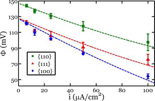
Nano Letters                                                                                                                                             Letter

various currents, and the response of the potential was                         crystalline silicon (c-Si) and amorphous lithiated silicon(a-
measured. To interpret these data, we have constructed a                        LiηSi) for all three orientations. This result agrees in part with a
kinetic model that considers three kinetic processes in series:                 previous work in which the boundary separating these two
the redox reaction at the electrolyte/lithiated silicon interface,              phases has been found to be atomically sharp for a {100}
the diffusion of lithium through the lithiated phase, and the                    wafer.29
chemical reaction at the lithiated silicon/crystalline silicon                    Figure 2 shows the measured plateau potentials as a function
interface. Using this model and experimental data, we can                       of the applied current density for all of the samples. The solid
determine which kinetic processes are the most important. In
particular, from our experiments we can quantify the rates of
reactions at the interfaces as a function of crystal orientation.
Additionally, we can provide a lower bound on the diffusivity of
lithium through the lithiated silicon phase. Using the measured
reaction rates, we have implemented a model of concurrent
reaction and plasticity into the finite element software
ABAQUS. This simulation accurately predicts anisotropic
morphological evolution and anisotropic fracture during initial
lithiation of crystalline silicon nanopillars of various axial
orientations.
   Figure 1 shows a typical response of the potential to a series
of applied currents for a {110} Si wafer. When a certain

                                                                                Figure 2. Measured potential versus Li/Li+, Φ, as a function of applied
                                                                                current density, i, for all three orientations. The solid symbols
                                                                                represent the mean of the tested samples, and the error bars represent
                                                                                ±1 standard deviation from the mean. The dashed lines represent fits
                                                                                from the kinetic model.

                                                                                symbols represent the mean of three samples for the given
                                                                                crystallographic orientation, and the error bars represent ±1
                                                                                standard deviation from the mean. The variation from sample
                                                                                to sample is quite small, demonstrating the reproducibility of
                                                                                the experiment.
                                                                                   Although Si transforms to numerous Li−Si crystalline phases
                                                                                at elevated temperatures,35 it has been shown that electro-
                                                                                chemical lithiation of Si at room temperature results in a
                                                                                metastable amorphous LiηSi phase, where η ≈ 3.5.36 It is likely
                                                                                that this phase exists over a finite range of lithium
                                                                                concentrations depending on the applied potential. However,
                                                                                assuming a composition of Li3.5Si and accounting for the
                                                                                corresponding volume expansion β = ΩLi3.5Si/ΩSi = 3.21,37 we
                                                                                have calculated the expected thickness for the current history
                                                                                corresponding to these experiments. These predicted thick-
                                                                                nesses were then compared to the measured thicknesses using
Figure 1. Typical sequence of applied current density, i, and measured          the SEM, and the values were in good agreement. Evidently, the
response of the potential versus Li/Li+, Φ, for a {110} Si wafer.
                                                                                velocity of the phase boundary is directly correlated with the
                                                                                applied current density. Hence, in our experiments one can
constant level of current density is applied for some duration of               think of the current density, for example, the horizontal axis in
time, the measured potential of Si vs Li/Li+ reaches a particular               Figure 2, as the velocity of the moving phase boundary. Thus,
value very quickly and remains at this value for the remainder of               Figure 2 shows that the {110} Si wafers are the “fastest” for a
the time. The measured potential provides information about                     given potential. For instance, at 120 mV vs Li/Li+ the
the concentration of lithium in the electrode at the interface                  interpolated average current densities for the {110}, {100},
with the electrolyte. For two-phase coexistence, lithium                        and {111} Si wafers are 47.1, 7.4, and 7.7 μA/cm2, respectively.
insertion is accommodated by the growth of the lithium-rich                     Such discrepancy in the velocities has important ramifications
phase at the expense of the lithium-poor phase. As a result, the                for lithiation of crystalline silicon structures with various crystal
concentration in the electrode at the interface with the                        facets exposed. For instance, these measurements of varying
electrolyte is fixed, rendering the potential constant in time                   phase boundary velocities can accurately account for aniso-
for a constant current density. These two-phase plateaus are                    tropic morphologies and fracture patterns developed in
evident for all three tested orientations (Figure 1, Supporting                 crystalline silicon nanopillars of various axial orientations, as
Information Figures S1, S2), suggesting the coexistence of                      will be discussed later.
                                                                         5040                          dx.doi.org/10.1021/nl302841y | Nano Lett. 2012, 12, 5039−5047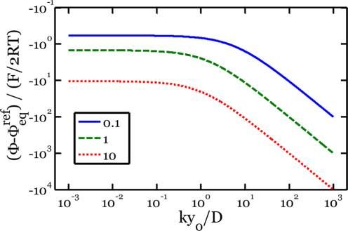
Nano Letters                                                                                                                                                   Letter

  Figure 3 illustrates an electrochemical cell in which                               LiηSi/c-Si interface. The three kinetic processes are concom-
crystalline silicon and metallic lithium react and form an                            itant and are in series; any of these processes may be rate-
amorphous phase of lithiated silicon                                                  limiting or they may occur at comparable rates such that
                                                                                      multiple processes govern the lithiation process.
   (η + δ)Li + Si = Li η + δSi                                          (1)              Associated with the redox reaction, Li+ + e− = Li, we take the
                                                                                      flux through the electrolyte/a-LiηSi interface, J1, as given by the
                                                                                      Butler−Volmer equation

                                                                                                 i 0 ⎡ ⎛ αF                    ⎞      ⎛ [1 − α]F
                                                                                         J1 =        ⎢exp⎜ −    [Φ − Φeq curr ]⎟ − exp⎜
                                                                                                 q ⎣ ⎝ RT                      ⎠      ⎝ RT
                                                                                                               ⎞⎤
                                                                                                [Φ − Φeq curr ]⎟⎥
                                                                                                               ⎠⎦                                                    (2)

                                                                                      where i0 is the exchange current density, q is the elementary
                                                                                      charge, α is the charge transfer coefficient, F is Faraday’s
                                                                                      constant, R is the ideal gas constant, T is the temperature, Φ is
                                                                                      the potential of the electrode (i.e., the measured voltage), and
Figure 3. In an electrochemical cell, crystalline silicon and lithium                 Φeqcurr is the equilibrium potential in the current state,
react at room temperature, forming an amorphous phase of lithiated
                                                                                      corresponding to the lithium concentration in the electrode
silicon. The concentrations C1 and C2 represent the concentration of
lithium in the lithiated silicon phase at the given interfaces. The dashed            near the electrolyte/a-LiηSi interface. Henceforth, we will use α
line represents the variation of the concentration of lithium as a                    = 1/2 for simplicity.
function of position in the Si electrode. The position in the a-Liη+δSi is               In the lithiated phase, η + δ is the number of lithium atoms
denoted by y and the total thickness of the layer by y0. The Ji denote                hosted by each silicon atom. We regard η as a constant and δ as
the fluxes of lithium at various positions: J1 at the interface between                a small deviation, δ ≪ η. As a result, the diffusion of lithium
the electrolyte and the lithiated silicon phase, J2 in the lithiated silicon          atoms in the lithiated silicon phase is driven by the position-
phase, J3 at the phase boundary between lithiated silicon and                         dependence of the composition, δ(y). Let C be the
crystalline silicon.                                                                  concentration of lithium in the lithiated phase (i.e., the amount
                                                                                      of lithium per unit volume of the lithiated phase). The
   The two electrodes are connected through a conducting wire                         concentration of lithium in this phase relates to the
and an electrolyte. The conducting wire may be connected to                           composition by C = (η + δ)/ΩLiηSi, where ΩLiηSi is the atomic
an external voltage source. At the interface between the metallic                     volume of the lithiated phase. We take the flux, J2, to be driven
lithium electrode and the electrolyte, lithium atoms dissociate                       by the gradient in the concentration of lithium through the
into lithium ions and electrons. Lithium ions pass through the                        thickness of the lithiated silicon
electrolyte while electrons pass through the conducting wire.
Upon reaching the silicon electrode, lithium ions and electrons                                      ∂C
recombine into lithium atoms. We expect that this latter                                 J2 = −D
                                                                                                     ∂y                                                              (3)
process occurs at the interface between the electrolyte and the
a-LiηSi, as the silicon samples have fairly large electric                            where D is the diffusivity of lithium in the lithiated silicon.
conductivity (see the Experimental Methods) and lithiated                             Because δ ≪ η, D is taken to be a constant, independent of the
silicon has even larger conductivity because of its metallic-like                     concentration. In the steady state, the flux is independent of the
properties.23,37 Lithium atoms then diffuse through the lithiated                      position, and the concentration varies linearly in the position,
silicon and react with the crystalline silicon (at the reaction                       so that J2 = D(C1 − C2)/y0, where C1 is the concentration of
front) to form fresh lithiated silicon, a-LiηSi. This process at the                  lithium in the lithiated silicon at the interface between the
c-Si/a-LiηSi interface involves breaking of silicon−silicon bonds                     electrolyte and the lithiated silicon, C2 is the concentration of
and formation of lithium−silicon bonds. Overall, this lithiation
                                                                                      lithium in the lithiated silicon at the interface between the
process causes lithiated silicon to grow at the expense of the
                                                                                      lithiated silicon and crystalline silicon phases, and y0 is the
crystalline silicon and metallic lithium.
                                                                                      thickness of the lithiated silicon.
   We now propose a model to quantify the relationship
                                                                                         At the interface between the lithiated silicon and the
between the measured potential and the applied current
                                                                                      crystalline silicon phases, a chemical reaction occurs, as given
density, accounting for the motion of the phase boundary. To
                                                                                      by eq 1. The reaction is driven by the excess lithium δ2 in the
do so, we adopt a modified version of the Deal−Grove model
                                                                                      lithiated silicon at this interface. The rate of reaction controls
for thermal oxidation of c-Si.38 In the model, the concentration
of lithium in the lithiated phase is a function of position, y                        the flux of lithium across the interface, and we take the
(Figure 3). We take the reference state as that of amorphous                          corresponding lithium flux to be given by the first-order relation
lithiated silicon of a given composition, LiηSi, in metastable                                     δ2
“equilibrium” with crystalline silicon. In the current state, the                        J3 = k
composition becomes Liη+δSi, where δ is a function of position                                    Ω Li ηSi                                                           (4)
y in the silicon electrode.
   Lithiation is driven by the externally applied voltage or                          where k is the rate of the reaction.
current density and involves three kinetic processes: the redox                          Using the Nernst equation, we can relate the equilibrium
reaction at the electrolyte/a-LiηSi interface, the diffusion of                        potential Φeqcurr to the excess lithium δ1 in the lithiated silicon
lithium through the a-LiηSi phase, and the reaction at the a-                         at the interface with the electrolyte
                                                                               5041                          dx.doi.org/10.1021/nl302841y | Nano Lett. 2012, 12, 5039−5047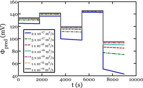
Nano Letters                                                                                                                                          Letter

                                   RT ⎡    δ1    ⎤                          that recovers the Butler−Volmer equation. It should be noted
    Φ − Φeq curr = Φ − Φeq ref +      ⎢          ⎥                          that the relative rates of diffusion and reaction at the a-LiηSi/c-
                                    F ⎣ η(η + 1) ⎦            (5)           Si interface are irrelevant in this limit. Instead, both of these
where Φeq is the equilibrium potential of a-LiηSi in the
           ref                                                              rates must be fast compared to the applied rate of insertion.
reference state (δ = 0).                                                    Once again, during a segment where the current density is
   With eqs 2−5, we can derive a relation between the applied               prescribed as a constant, the potential, Φ, is likewise a constant.
current density, i, and the measured potential, Φ, in the steady            This limit is known in literature as a process limited by the rate
state. For the full derivation of this relation, please see the             of the “surface reaction”.39
Supporting Information. The result of this derivation is:                      Figure 4 demonstrates the effects of varying the intrinsic
                                                                            dimensionless parameters ky0/D and i0ΩLiηSi/kqη for a fixed
               ⎧     ⎛
     i         ⎪  F ⎜                RT ⎡ Ω Li ηSi
       = 2 sinh⎨−    ⎜ Φ − Φ   ref
                                   +     ⎢
                                      F ⎢⎣ qη(η + 1)
               ⎪            eq
    i0         ⎩ 2RT ⎝
         ⎛   ky ⎞ 1 ⎤⎞⎪⎫
         ⎜1 + 0 ⎟ i ⎥⎟⎟⎬
         ⎝    D ⎠ k ⎥⎦⎠⎪
                       ⎭                                      (6)
   It is important to note that there are three intrinsic time
scales in this model: qy0η/i0ΩLiηSi, y02/D, and y0/k, associated
with the electrolyte/electrode surface reaction, the diffusion
through the a-LiηSi layer, and the reaction at the a-LiηSi/c-Si
interface. There is also a time scale qy0η/iΩLiηSi associated with
the applied current density. These four time scales form three
dimensionless groups: i0ΩLiηSi/kqη, ky0/D, and i/i0. The
parameter ky0/D characterizes the relative rates of reaction at
the a-LiηSi/c-Si interface and diffusion through the a-LiηSi
phase. If ky0/D ≫ 1, the reaction at the a-LiηSi/c-Si interface is          Figure 4. Potential predicted from kinetic model as a function of the
fast, and eq 6 becomes                                                      dimensionless constant ky0/D. The various curves represent different
               ⎧     ⎛                                                      values of the dimensionless constant i0ΩLiηSi/kqη. In this simulation, i/
     i         ⎪  F ⎜                RT                                     i0 = 1.
       = 2 sinh⎨−    ⎜ Φ − Φeq ref +
    i0         ⎪
               ⎩ 2RT ⎝                F
                                                                            value i/i0 = 1. To produce this figure, we have solved eq 6 for
         ⎡ Ω Li Si y ⎤⎞⎪   ⎫                                                the potential, Φ, for given values of the dimensionless
                      0 ⎟
         ⎢       η
                       i ⎥⎟⎬                                                constants. The various curves represent different values of the
         ⎢⎣ qη(η + 1) D ⎥⎦⎠⎪
                           ⎭                                  (7)           dimensionless constant i0ΩLiηSi/kqη. During an electrochemical
.                                                                           experiment at a constant current density, the thickness of the
   During a segment where the current density is prescribed as a            lithiated layer, y0, will increase in time. Thus, the horizontal axis
constant, the thickness of the lithiated layer, y0, increases with          is representative of time during such an experiment. The
time. As a result, the potential, Φ, decreases with time. Such              transition from a reaction-controlled to a diffusion-controlled
behavior is indeed observed in numerous electrochemical                     process can clearly be seen as ky0/D increases. Also, larger
experiments, including the lithiation of amorphous sputtered                values of i0ΩLiηSi/kqη indicate a slower rate of reaction at the
silicon, and is indicative of a diffusion-limited process.                   interface between the lithiated silicon and the crystalline silicon,
   In contrast, if ky0/D ≪ 1, the diffusion of lithium through the           which results in larger values of overpotential, |Φ−Φeqref |.
lithiated phase is fast, and eq 6 becomes                                      We should also remark that within this model it is impossible
                                                                            to separate the contributions of the reactions at each interface
               ⎧     ⎛                                    ⎞⎫
     i         ⎪  F ⎜                RT ⎡ Ω Li ηSi 1 ⎤⎟⎪                    from a single experiment. This is evident if we take the further
       = 2 sinh⎨−    ⎜ Φ − Φ   ref
                                   +     ⎢            i ⎥  ⎬                limit of eq 8 for which i ≪ i0
                                      F ⎢⎣ qη(η + 1) k ⎥⎦⎟⎠⎪
               ⎪            eq
    i0         ⎩ 2RT ⎝                                     ⎭
                                                                                                  RT ⎡ Ω Li ηSi 1    1⎤
                                                              (8)               Φ − Φeq ref = −       ⎢             + ⎥i
   Here, we take the reaction-rate, k, along a given crystal                                       F ⎢⎣ qη(η + 1) k  i0 ⎥⎦                                 (10)
direction as a constant. In this limit, during a segment where              .
the current density is prescribed as a constant, the potential, Φ,             From eq 10, it is clear that if one reaction is much faster than
is likewise a constant. This observation is consistent with the             the other, the measured relation between i and Φ gives
previous discussion concerning our observed plateaus in                     information on the slower process. If both contributions in
potential, that is, this reaction-limited situation corresponds             brackets are comparable, a single measurement relating i and Φ
to a moving phase boundary.                                                 does not give distinct information on both i0 and k. It may be
   Another possible limit of eq 6 occurs when the applied                   possible, however, to quantify the individual contributions of
current density is very small such that {[ΩliηSi/qη(η + 1)](1 +             the reactions at these interfaces from a set of multiple
kyo/D)(1/k)i} ≪ 1, giving                                                   experiments in which one of these parameters is constant (or
     i         ⎡ F                   ⎤                                      does not exist). For instance, one could measure the velocity of
       = 2 sinh⎢ −     (Φ − Φeq ref )⎥                                      the phase boundary in lithium−silicon diffusion couples for
    i0         ⎣   2RT               ⎦                        (9)           silicon wafers of various orientations. This experiment would
                                                                     5042                           dx.doi.org/10.1021/nl302841y | Nano Lett. 2012, 12, 5039−5047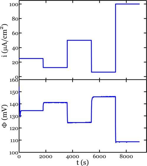
Nano Letters                                                                                                                                               Letter

give information on the parameter k, as the parameter i0                      produce a relationship between the applied current densities
associated with the redox reaction is unimportant. In another                 and predicted potentials. We have then performed a least-
experiment, amorphous silicon samples could be examined. In                   squares fit between the measured and predicted potentials to
these amorphous silicon samples, the electrode is a single phase              find the appropriate values of k for each orientation and i0. The
with a continuous variation in the lithium concentration during               parameters used in this simulation are given in Table 1. The
lithiation. Hence, only diffusion and the redox reaction at the
electrolyte/electrode contribute to the kinetics of the insertion             Table 1. Parameters Used in Simulations and Calculated
process. Thus, experiments could be performed to carefully                    Resultsa
characterize i0(C) near the compositions of interest. Fur-
                                                                                          parameter                                        value
thermore, a set of multiple experiments in which i0 is a constant
but k varies would give information on both parameters. We                              T                                          20 °C
believe this latter situation applies to our experiments, as k                          η                                          3.536
depends on the crystallographic orientation, while i0 is the same                       ΩLi3.5Si                                   6.91 × 10⁻²⁹ m3 37
during each experiment.                                                                 Φeqref: ⟨110⟩                              149.2 ± 2.33 mV
   We now apply the kinetic model to our experimental data.                             Φeqref: ⟨111⟩                              129.4 ± 2.41 mV
Upon close examination of all of our data, we have found that                           Φeqref: ⟨100⟩                              128.3 ± 3.05 mV
the majority of the nonzero constant current segments produce                           β = ΩLiηSi/ΩSi                             3.2137
extremely flat profiles in potential with time (see for instance,                         σY                                         1 GPa18
Figure 1). The only exception to flat potential profiles occurred                         ESi                                        160 GPa46
in some of the {100} and {111} samples during the largest                               ELiηSi                                     12 GPa47
current density used, 100 μA/cm2. In these anomalous                                    νSi = νLiηSi                               0.2246
segments, the potential increased with time (Supporting                                 i0*                                        0.45   A/m2
Information Figures S1, S2). As mentioned in the previous                               k: ⟨110⟩*                                  1.63   × 10−10 m/s
section, if the lithiation process were controlled by diffusion                          k: ⟨111⟩*                                  7.05   × 10−11 m/s
through the lithiated silicon phase, the potential would decrease                       k: ⟨100⟩*                                  2.54   × 10−11 m/s
with time. Thus, we do not believe that the lithiation process is             a
                                                                               Results calculated from a fit of the model to the experimental data are
controlled by diffusion during these segments. We are uncertain                denoted by *.
about the precise origin of these upward sloping potentials,
although they may correspond to some lithium from a-LiηSi                     value used for η is a representative value found in other
being consumed by the formation of solid electrolyte interphase               experiments under similar conditions.36 Although this number
(SEI).                                                                        may not be entirely accurate for our experiments, changing the
   The data in Figure 2 and other experiments also suggest                    value of η will only scale the predicted value of k by some
anisotropy in lithiation of crystalline silicon.30−32 Recalling that          constant numerical factor and will not affect the relative values
the lithiated phase is amorphous, it is difficult to imagine a                  of k for the various orientations. Also, the equilibrium potentials
source of anisotropy if the kinetics of the lithiation process were           used in the simulation are the instantaneous values measured
dominated by the reduction reaction at the electrolyte/a-LiηSi                during the open circuit voltage segments in our experiments. It
interface. One may argue that the redox reaction depends on                   is important to note that the equilibrium potential associated
the nature of the SEI that forms between the electrolyte and the              with the {110} Si is approximately 20 mV larger than the other
specific electrode, potentially leading to anisotropy. However, it             two orientations.
seems improbable that the structure and composition of this                      The results of this fit are shown in Table 1. Using these
SEI are strongly affected by the crystal orientation of the silicon,           values, the predicted relationships between potential and
as the lithiated silicon side of this interface becomes amorphous             current density are shown as dashed lines in Figure 2. The
during the early stages of the lithiation process. In contrast,               predictions from the fit agree well with the data. Both the
anisotropy seems natural if the reaction at the a-LiηSi/c-Si                  calculated reaction rate at the a-LiηSi/c-Si interface and the
interface contributes to the overall kinetics of the lithiation               measured equilibrium potential are largest for {110} Si. Each of
process. For this reaction to advance, cooperative rearrange-                 these characteristics contributes to the phase boundary moving
ment of atoms must occur, involving breaking and reforming                    “fastest” in the ⟨110⟩ direction for a given potential.
bonds. Surfaces of silicon in various crystallographic orienta-                  In the model, we have assumed a metastable equilibrium
tions have drastically different atomic structures, which can                  state, Li3.5Si, as motivated by the observations of Li et al.36 For
readily result in different rates of reaction on these different                small deviations from this composition, we can treat the
surfaces. For instance, such anisotropy has been observed in the              quantities γ, D, i0, and k as constants, independent of the
rate of thermal oxidation of silicon of various crystal                       concentration of lithium in the lithiated silicon phase. As a
orientations.40,41 Thus, we believe that the reaction at the a-               particular example, with the assumption that the lithiated phase
LiηSi/c-Si interface must contribute to the observed relation-                is Li3.5Si, we would expect the measured equilibrium potentials
ship between current density and potential as shown in Figure                 during open-circuit segments to be independent of the crystal
2.                                                                            orientation of the silicon. It was found, however, that the
   As previously mentioned, it is impossible to separate the                  equilibrium potential for {110} Si was about 20 mV larger than
contributions of the reactions at each interface from a single                for the other two orientations. It is possible that this
experiment. However, we believe that i0 is independent of                     discrepancy is due to a slightly different composition existing
crystal orientation, while k is a function of crystal orientation.            in the amorphous phase during the experiments on {110} Si.
Since we have experiments for various crystal orientations of                 For instance, if the rate of the reaction at the a-LiηSi/c-Si
the silicon, we can fit both i0 and k. To do so, we have written               interface for {110} Si is fast compared to the insertion rate (i.e.,
in a program in Matlab to solve eq 8 for a given k and i0 to                  applied current density), then the concentration of lithium in
                                                                       5043                              dx.doi.org/10.1021/nl302841y | Nano Lett. 2012, 12, 5039−5047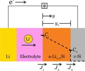
Nano Letters                                                                                                                                              Letter

the lithiated phase may be slightly smaller than that of the                      room temperature.42 Similarly, Xie et al. found a value of 3 ×
{100} and {111} orientations. This effect would result in a                        10−17−3 × 10⁻¹⁶ m2/s for sputtered amorphous silicon films
larger measured equilibrium potential, Φeqref, for {110} Si                       using EIS at 20 °C.43
compared to the other orientations, which is consistent with the                     As a final comment, we have seen no evidence of diffusion-
experiments. Such dependence of the composition of the                            limited kinetics despite having lithiated samples to thicknesses
metastable phase on the orientation of the crystalline phase is                   on the order of micrometers. In contrast, typical nanostructured
not considered in our model; Φeqref is simply taken as an input                   electrodes of silicon have feature sizes less than a few hundred
parameter measured from our experiments. This interplay may                       nanometers.7,9,14,15,44 Thus, under normal operating conditions,
be important for the lithiation process, however, as it further                   lithiation of crystalline silicon will be limited by the reaction of
amplifies the anisotropy along different crystal directions. Thus,                  silicon and lithium at the reaction front, rather than by the
once functions such as γ(C), D(C), i0(C), and so forth are more                   diffusion of lithium through the amorphous phase.
carefully characterized, they can be incorporated into the                           We now use the measured velocities of the reaction fronts to
kinetic model to make it more complete. Still, we believe that                    quantify recent experimental observations. This analysis is
the important physics associated with the initial lithiation of                   performed under the framework of a previously developed
crystalline silicon have been captured in our kinetic model.                      model of concurrent reaction and plasticity; for more on this
   The model also provides some information of the value of                       model, please see ref 33. The concurrent reaction and plasticity
the diffusivity of lithium in amorphous silicon. As discussed                      are simulated using the finite element program ABAQUS.
previously, it is evident from the flat potential profiles that                     Within the context of the program, the lithiation-induced
diffusion through the lithiated phase is not the rate-limiting                     volumetric expansion is simulated as thermal expansion, while
step. Using the values from the fit for i0 and k, however, we can                  deformation in the lithiated silicon is modeled by the elastic-
substitute various values of D into eq 6 and evaluate the effect                   plastic theory (J2 plasticity).45 The crystalline silicon is modeled
on the potential profiles. The results are shown in Figure 5,                      as an elastic material. To simulate the movements of the
                                                                                  reaction fronts, we prescribe a moving temperature field. To
                                                                                  avoid computational singularity, the temperature front, which
                                                                                  simulates the reaction front, is located within a thin shell, whose
                                                                                  size is much smaller than the feature size of the nanopillar but is
                                                                                  sufficiently larger than the mesh size. Such regularization is used
                                                                                  to afford a compromise between computational cost and
                                                                                  accuracy.
                                                                                     To illustrate this model in combination with our
                                                                                  experimental data, we simulate the morphological evolution
                                                                                  and stress development during the lithiation of crystalline
                                                                                  silicon nanopillars of various axial orientations.32 The black
                                                                                  lines in the second column of Figure 6 show the crystal
                                                                                  orientations of the sidewalls of these silicon nanopillars. The
                                                                                  velocities of the fronts depend on the crystallographic
                                                                                  orientation, with values given by our experiments at 120 mV
Figure 5. Predicted potential response versus Li/Li+, Φpred, for a {110}          (so-called “partial lithiation” by Lee et al.32). In particular, at
Si wafer with initial lithiated thickness of 1 μm subject to the current
                                                                                  this potential the relative velocities were found to be V⟨110⟩ =
loading shown in Figure 1. The various curves represent different
hypothetical values of the diffusivity of lithium through the lithiated            6.4V⟨100⟩ = 6.1V⟨111⟩. It is important to note that within this
silicon phase.                                                                    model, the absolute velocities of the reaction fronts are not
                                                                                  important in developing the stress and deformation fields; only
                                                                                  the relative velocities matter. In this simulation, we have used
where it is evident that the potential profiles would look                         the following parameters: β = ΩLiηSi/ΩSi = 3.21,37 σY = 1 GPa,18
drastically different if the diffusivity were as slow as 2 × 10⁻¹⁷
                                                                                  ESi = 160 GPa,46 ELiηSi = 12 GPa,47 νSi = νLiηSi = 0.22.46 It should
m2/s. In comparison to the reaction-limited case, the measured
potentials would be much smaller and would create profiles                         be noted that the modulus and Poisson’s ratio of the crystalline
decreasing with time. Moreover, these slopes would increase in                    Si phase are taken as independent of orientation. This
absolute value with current density, as given by eq 6. If we                      approximation is made for simplicity of implementation into
applied our kinetic model to a system that is rate-limited by                     the ABAQUS model. The modulus used for the crystalline
diffusion through the electrode, we could fit eq 6 to the data to                   phase is that of polycrystalline silicon, which is a representative
measure the value of diffusivity but as previously discussed, the                  modulus of the core in an average sense. The pillars are
overall kinetic process does not seem to be limited by diffusion                   modeled using plane−strain conditions, as motivated by
through the amorphous layer during the initial lithiation of                      experimental observations of a lack of growth in the axial
crystalline silicon. The results in Figure 5 can be used to                       direction.32 Figure 6 shows the stress and morphology of the
estimate a lower bound on the diffusivity. Bearing in mind that                    nanopillars after partial lithiation simulated using the procedure
the actual data are similar to the solid gray line in Figure 5, a                 described above. The simulated anisotropic patterns agree
reasonable estimate of the lower bound for the diffusivity of                      extremely well with the experimental observations.32
lithium in a-Li3.5Si is D = 2 × 10⁻¹⁶ m2/s. In comparison to                         Recently, it has been observed that under certain conditions
values in the literature, Ding et al. found a value of 1 × 10⁻¹⁶                  these nanopillars will fracture anisotropically.48 Moreover, Lee
m2/s for nanocrystalline silicon particles using the galvanostatic                et al. surmised that this anisotropic fracture results from stress
intermittent titration technique (GITT), cyclic voltammetry                       concentrations due to the anisotropic expansion of the
(CV), and electrochemical impedance spectroscopy (EIS) at                         nanopillars.48 Here, we quantify this idea using ABAQUS and
                                                                           5044                         dx.doi.org/10.1021/nl302841y | Nano Lett. 2012, 12, 5039−5047
Nano Letters Letter
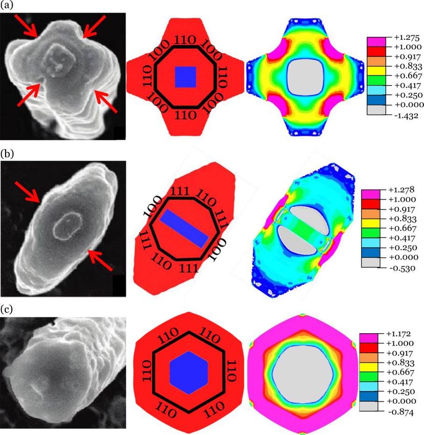
Figure 6. Comparison between experiments and finite element simulation of lithiation of crystalline silicon nanopillars of various axial orientations:
(a) ⟨100⟩, (b) ⟨110⟩, and (c) ⟨111⟩. The first column shows the experimentally observed morphology after lithiation from Lee et al.32 The red
arrows indicate the fracture sites observed most frequently in experiments.47 The second column shows simulated morphology at a certain stage of
lithiation. The fully lithiated phase is given in red while the crystalline silicon phase is shown in blue. The black outline shows the initial shape in the
simulation and the corresponding orientations of the crystal facets. The third column shows the maximum in plane stress at the same stage of
lithiation. The pink regions have stresses exceeding the yield strength. The legend shows the stress in units of GPa.
our experimentally measured reaction front velocities. In Figure In conclusion, silicon can host a large amount of lithium,
6, we observe that for the ⟨100⟩ and ⟨111⟩ nanopillars the making it one of the most promising materials for anodes.
maximum principal tensile stress occurs at the locations midway Crystalline silicon is of particular importance due to its use in
between neighboring {110} planes. These locations are recent anode architectures such as nanowires, nanoporous
consistent with the fracture locations most frequently observed structures, thin films, nanoparticles, and so forth. In this study,
in the work of Lee et al.48 Furthermore, we observe that the we have performed electrochemical experiments on {100},
maximum tensile stress can exceed the yield strength due to the {110}, and {111} crystalline silicon wafers. These experiments
triaxiality of the state of stress at these locations. In the indicate the existence of a moving phase boundary for all three
simulation of the ⟨111⟩ nanopillar, the state of stress was found orientations, indicating that short-range processes at the a-
to be approximately axisymmetric, implying that there should LiηSi/c-Si interface significantly contribute to the kinetics of the
be little anisotropy in the locations of fracture. In the work of lithiation process. The velocity of this phase boundary was
Lee et al., fracture was indeed observed at arbitrary locations found to be faster for {110} silicon than for the other
albeit with a slightly higher incidence at locations between the orientations. Using the measured velocities, we have
{110} planes.48 Thus, our simulations agree quite well with implemented a model of concurrent reaction and plasticity
their experiments. into ABAQUS. This simulation accurately accounts for
5045 dx.doi.org/10.1021/nl302841y | Nano Lett. 2012, 12, 5039−5047Nano Letters Letter
anisotropic morphologies and fracture patterns developed in such as continuous growth of the solid electrolyte interphase
crystalline silicon nanopillars of various axial orientations. affects the measured potentials in a time-dependent manner. It
Furthermore, we have presented a kinetic model accounting for is possible that the effect of the SEI is minimized because most
the redox reaction at the electrolyte/a-LiηSi interface, diffusion of the growth may occur during the initial 5 h current segment.
through the a-LiηSi, and the chemical reaction at the a-LiηSi/ Still, it is important to note that the SEI will form during this
crystalline silicon interface. From this model, we have experiment. This growth process may be different from cell to
quantified the rates of reactions at the interfaces and have cell and may be one source of variation in the measured
provided a lower bound for the diffusivity through the lithiated potentials from sample to sample. Additionally, it has been
silicon phase. We believe that this model accounts for the shown that below a potential of about 50 mV versus Li/Li+,
pertinent physics in electrodes that undergo two-phase amorphous LiηSi transforms to crystalline Li3.75Si.36 Thus, in an
coexistence and will have further value beyond the silicon attempt to avoid this amorphous to crystalline phase trans-
system. Thus, we hope this model will provide guidance for the formation, the applied currents were selected such that the
design of future experiments and atomistic simulations. potential is maintained above 50 mV versus Li/Li+.
Experimental Methods. Silicon wafers of three orienta- To image the phase boundary, the samples were removed
tions, {100}, {110}, and {111}, were used as the working from the cell in the glovebox, rinsed in DEC, dried, and broken
electrodes. The wafers were all doped with phosphorus and had into fragments. These fragments were sealed in a container in
similar and low resistivity (5−10 Ω·cm). Because of the low the glovebox and immediately transferred to the SEM chamber.
resistivity, the maximum ohmic drop in potential through the It was estimated that they were exposed to air for less than two
thickness of the wafer was calculated to be less than 50 μV for minutes during the transfer process.
the current densities used in these experiments. The {100} and
{110} wafers were 500 μm thick, and the {111} wafer was 250
μm thick. The wafers were cut into 6 cm × 1 cm sections.
■
*
ASSOCIATED CONTENT
S Supporting Information
The samples were cleaned with acetone and isopropanol.
Next, they were placed into a sputter deposition system (AJA Additional figures. This material is available free of charge via
the Internet at http://pubs.acs.org.
■
Int. ATC 1800). All sputtering targets used had a 50.8 mm
diameter, and depositions were performed at room temperature
(22 °C). First, the samples were plasma-cleaned in Ar at 20 AUTHOR INFORMATION
mTorr and 24 W (RF) for 5 min. Then, a 50 nm thick layer of Corresponding Author
Ti was deposited, 3 mTorr of Ar at 100 W (DC) for 5 min, *E-mail: vlassak@seas.harvard.edu.
followed by a 250 nm layer of Cu, 5 mTorr of Ar at 200 W
Notes
(DC) for 12.5 min. These layers serve as the current collector.
The authors declare no competing financial interest.
■
On top of these layers, 500 nm of Si3N4 was deposited using
plasma-enhanced chemical vapor deposition (Nexx Cirrus 150
PECVD) to prevent electrochemical reaction of Li with the Cu ACKNOWLEDGMENTS
and Ti layers. During PECVD, a small region of the Cu layer This work is supported by the National Science Foundation
was masked to allow for electrical contact with the electrode. It through a grant on Lithium-ion Batteries (CMMI-1031161).
was observed in control experiments that no significant This work was performed in part at the Center for Nanoscale
electrochemical signal was produced for an electrode coated Systems (CNS), a member of the National Nanotechnology
with 500 nm of Si3N4; thus, the nitride served its purpose as a Infrastructure Network (NNIN), which is supported by the
passivating layer. National Science Foundation under NSF Award No. ECS-
Electrochemical cells were assembled in a glovebox (Vacuum 0335765. C.N.S. is part of Harvard University. M.P. acknowl-
Atmospheres HE-43) in an ultrahigh purity Ar atmosphere with edges government support under and awarded by DoD, Air
less than 0.1 ppm moisture content. The Si wafer was Force Office of Scientific Research, National Defense Science
incorporated as the working electrode into a homemade and Engineering Graduate (NDSEG) Fellowship, 32 CFR
three-electrode electrochemical cell with lithium foil used as the 168a.
■
counter and reference electrodes. One molar LiPF6 in 1:1 (vol
%) ethylene carbonate (EC)/diethyl carbonate (DEC) was REFERENCES
used as the electrolyte (Novolyte Technologies). The cells were
(1) Armand, M.; Tarascon, J. M. Nature 2008, 451 (7179), 652−657.
hermetically sealed inside the glovebox using paraffin wax and (2) Service, R. F. Science 2011, 332 (6037), 1494−1496.
tested using a VersaSTAT 3 potentiostat (Princeton Applied (3) Ellis, B. L.; Lee, K. T.; Nazar, L. F. Chem. Mater. 2010, 22 (3),
Research) outside of the glovebox. The wafers were initially 691−714.
lithiated at a constant current density of 12.5 μA/cm2 for 5 h (4) Marom, R.; Amalraj, S. F.; Leifer, N.; Jacob, D.; Aurbach, D. J.
followed by four other current densities: 6.25, 25, 50, and 100 Mater. Chem. 2011, 21 (27), 9938−9954.
μA/cm2 applied in random order for 1 h each with a 30 min (5) Zhang, W. J. J. Power Sources 2011, 196 (1), 13−24.
open-circuit segment between each imposed current density. (6) Beaulieu, L. Y.; Eberman, K. W.; Turner, R. L.; Krause, L. J.;
To observe time-dependent effects in the experiments, all five Dahn, J. R. Electrochem. Solid-State Lett. 2001, 4 (9), A137−A140.
current densities were then applied again (also in random (7) Chan, C. K.; Peng, H. L.; Liu, G.; McIlwrath, K.; Zhang, X. F.;
Huggins, R. A.; Cui, Y. Nat. Nanotechnol. 2008, 3 (1), 31−35.
order) for 30 min each. Finally, an open-circuit segment was
(8) Peng, K. Q.; Jie, J. S.; Zhang, W. J.; Lee, S. T. Appl. Phys. Lett.
applied for 30 min. For each sample, the two values of the 2008, 93 (3), 033105.
measured potential corresponding to each current density were (9) Takamura, T.; Ohara, S.; Uehara, M.; Suzuki, J.; Sekine, K. J.
observed to be quite similar (usually within 1 mV), Power Sources 2004, 129 (1), 96−100.
demonstrating that the results are quite reproducible. In (10) Haftbaradaran, H.; Xiao, X. C.; Verbrugge, M. W.; Gao, H. J. J.
other words, it does not seem that a time-dependent process Power Sources 2012, 206, 357−366.
5046 dx.doi.org/10.1021/nl302841y | Nano Lett. 2012, 12, 5039−5047Nano Letters Letter
(11) Yu, C. J.; Li, X.; Ma, T.; Rong, J. P.; Zhang, R. J.; Shaffer, J.; An, (41) Kao, D. B.; McVittie, J. P.; Nix, W. D.; Saraswat, K. C. IEEE
Y. H.; Liu, Q.; Wei, B. Q.; Jiang, H. Q. Adv. Energy Mater. 2012, 2 (1), Trans. Electron Devices 1987, 34 (5), 1008−1017.
68−73. (42) Ding, N.; Xu, J.; Yao, Y. X.; Wegner, G.; Fang, X.; Chen, C. H.;
(12) Soni, S. K.; Sheldon, B. W.; Xiao, X. C.; Tokranov, A. Scr. Mater. Lieberwirth, I. Solid State Ionics 2009, 180 (2−3), 222−225.
2011, 64 (4), 307−310. (43) Xie, J.; Imanishi, N.; Zhang, T.; Hirano, A.; Takeda, Y.;
(13) Soni, S. K.; Sheldon, B. W.; Xiao, X. C.; Verbrugge, M. W.; Ahn, Yamamoto, O. Mater. Chem. Phys. 2010, 120 (2−3), 421−425.
D.; Haftbaradaran, H.; Gao, H. J. J. Electrochem. Soc. 2012, 159 (1), (44) Yamada, M.; Ueda, A.; Matsumoto, K.; Ohzuku, T. J.
A38−A43. Electrochem. Soc. 2011, 158 (4), A417−A421.
(14) Baggetto, L.; Danilov, D.; Notten, P. H. L. Adv. Mater. 2011, 23 (45) Hill, R. The Mathematical Theory of Plasticity; Oxford University
(13), 1563−1566. Press: Oxford, 1950.
(15) Yao, Y.; McDowell, M. T.; Ryu, I.; Wu, H.; Liu, N. A.; Hu, L. B.; (46) Freund, L. B.; Suresh, S. Thin Film Materials: Stress, Defect
Nix, W. D.; Cui, Y. Nano Lett. 2011, 11 (7), 2949−2954. Formation and Surface Evolution; Cambridge University Press:
(16) Wu, H.; Chan, G.; Choi, J. W.; Ryu, I.; Yao, Y.; McDowell, M. Cambridge, U.K., 2003.
T.; Lee, S. W.; Jackson, A.; Yang, Y.; Hu, L. B.; Cui, Y. Nat. (47) Hertzberg, B.; Benson, J.; Yushin, G. Electrochem. Commun.
Nanotechnol. 2012, 7 (5), 309−314. 2011, 13 (8), 818−821.
(17) Hertzberg, B.; Alexeev, A.; Yushin, G. J. Am. Chem. Soc. 2010, (48) Lee, S. W.; McDowell, M. T.; Berla, L. A.; Nix, W. D.; Cui, Y.
132 (25), 8548−+. Proc. Natl. Acad. Sci. U.S.A. 2012, 109 (11), 4080−4085.
(18) Sethuraman, V. A.; Chon, M. J.; Shimshak, M.; Srinivasan, V.;
Guduru, P. R. J. Power Sources 2010, 195 (15), 5062−5066.
(19) Huang, J. Y.; Zhong, L.; Wang, C. M.; Sullivan, J. P.; Xu, W.;
Zhang, L. Q.; Mao, S. X.; Hudak, N. S.; Liu, X. H.; Subramanian, A.;
Fan, H. Y.; Qi, L. A.; Kushima, A.; Li, J. Science 2010, 330 (6010),
1515−1520.
(20) Zhao, K. J.; Pharr, M.; Cai, S. Q.; Vlassak, J. J.; Suo, Z. G. J. Am.
Ceram. Soc. 2011, 94, S226−S235.
(21) Zhao, K. J.; Pharr, M.; Vlassak, J. J.; Suo, Z. G. J. Appl. Phys.
2011, 109 (1), 016110.
(22) Bower, A. F.; Guduru, P. R.; Sethuraman, V. A. J. Mech. Phys.
Solids 2011, 59 (4), 804−828.
(23) Wan, W. H.; Zhang, Q. F.; Cui, Y.; Wang, E. G. J. Phys.:
Condens. Matter 2010, 22 (41), 415501.
(24) Zhao, K. J.; Wang, W. L.; Gregoire, J.; Pharr, M.; Suo, Z. G.;
Vlassak, J. J.; Kaxiras, E. Nano Lett. 2011, 11 (7), 2962−2967.
(25) Obrovac, M. N.; Christensen, L. Electrochem. Solid-State Lett.
2004, 7 (5), A93−A96.
(26) Li, H.; Huang, X. J.; Chen, L. Q.; Zhou, G. W.; Zhang, Z.; Yu, D.
P.; Mo, Y. J.; Pei, N. Solid State Ionics 2000, 135 (1−4), 181−191.
(27) Key, B.; Bhattacharyya, R.; Morcrette, M.; Seznec, V.; Tarascon,
J. M.; Grey, C. P. J. Am. Chem. Soc. 2009, 131 (26), 9239−9249.
(28) Key, B.; Morcrette, M.; Tarascon, J. M.; Grey, C. P. J. Am. Chem.
Soc. 2011, 133 (3), 503−512.
(29) Chon, M. J.; Sethuraman, V. A.; McCormick, A.; Srinivasan, V.;
Guduru, P. R. Phys. Rev. Lett. 2011, 107 (4), 045503.
(30) Liu, X. H.; Zheng, H.; Zhong, L.; Huan, S.; Karki, K.; Zhang, L.
Q.; Liu, Y.; Kushima, A.; Liang, W. T.; Wang, J. W.; Cho, J. H.;
Epstein, E.; Dayeh, S. A.; Picraux, S. T.; Zhu, T.; Li, J.; Sullivan, J. P.;
Cumings, J.; Wang, C. S.; Mao, S. X.; Ye, Z. Z.; Zhang, S. L.; Huang, J.
Y. Nano Lett. 2011, 11 (8), 3312−3318.
(31) Goldman, J. L.; Long, B. R.; Gewirth, A. A.; Nuzzo, R. G. Adv.
Funct. Mater. 2011, 21 (13), 2412−2422.
(32) Lee, S. W.; McDowell, M. T.; Choi, J. W.; Cui, Y. Nano Lett.
2011, 11 (7), 3034−3039.
(33) Zhao, K. J.; Pharr, M.; Wan, Q.; Wang, W. L.; Kaxiras, E.;
Vlassak, J. J.; Suo, Z. G. J. Electrochem. Soc. 2012, 159 (3), A238−A243.
(34) Yang, H.; Huang, S.; Huang, X.; Fan, F. F.; Liang, W. T.; Liu, X.
H.; Chen, L. Q.; Huang, J. Y.; Li, J.; Zhu, T.; Zhang, S. L. Nano Lett.
2012, 12 (4), 1953−1958.
(35) Boukamp, B. A.; Lesh, G. C.; Huggins, R. A. J. Electrochem. Soc.
1981, 128 (4), 725−729.
(36) Li, J.; Dahn, J. R. J. Electrochem. Soc. 2007, 154 (3), A156−A161.
(37) Zhao, K. J.; Tritsaris, A. G.; Pharr, M.; Wang, W. L.; Okeke, O.;
Suo, Z. G.; Vlassak, J. J.; Kaxiras, E. Nano Lett. 2012, 12 (8), 4397−
4403.
(38) Deal, B. E.; Grove, A. S. J. Appl. Phys. 1965, 36 (12), 3770−&.
(39) Li, J. C.; Xiao, X. C.; Yang, F. Q.; Verbrugge, M. W.; Cheng, Y.
T. J. Phys. Chem. C 2012, 116 (1), 1472−1478.
(40) Gonzalez, C.; McVittie, J. P. IEEE Electron Device Lett. 1985, 6
(5), 215−218.
5047 dx.doi.org/10.1021/nl302841y | Nano Lett. 2012, 12, 5039−5047You can also read