Molecular embroidering of graphene - ARTICLE - Nature
←
→
Page content transcription
If your browser does not render page correctly, please read the page content below
ARTICLE
                  https://doi.org/10.1038/s41467-020-20651-w                OPEN

                  Molecular embroidering of graphene
                  Tao Wei         1,   Malte Kohring2, Heiko B. Weber                 2,   Frank Hauke1 & Andreas Hirsch                    1✉

                  Structured covalent two-dimensional patterning of graphene with different chemical func-
                  tionalities constitutes a major challenge in nanotechnology. At the same time, it opens
                  enormous opportunities towards tailoring of physical and chemical properties with limitless
1234567890():,;

                  combinations of spatially defined surface functionalities. However, such highly integrated
                  carbon-based architectures (graphene embroidery) are so far elusive. Here, we report a
                  practical realization of molecular graphene embroidery by generating regular multiply func-
                  tionalized patterns consisting of concentric regions of covalent addend binding. These spa-
                  tially resolved hetero-architectures are generated by repetitive electron-beam lithography/
                  reduction/covalent-binding sequences starting with polymethyl methacrylate covered gra-
                  phene deposited on a Si/SiO2 substrate. The corresponding functionalization zones carry
                  bromobenzene-, deutero-, and chloro-addends. We employ statistical Raman spectroscopy
                  together with scanning electron microscopy/energy dispersive X-ray spectroscopy for an
                  unambiguous characterization. The exquisitely ordered nanoarchitectures of these covalently
                  multi-patterned graphene sheets are clearly visualized.

                  1 Department  of Chemistry and Pharmacy & Joint Institute of Advance Materials and Processes (ZMP), Friedrich-Alexander University of Erlangen-
                  Nuremberg (FAU), Nikolaus-Fiebiger-Strasse 10, 91058 Erlangen, Germany. 2 Department of Applied Physics & Institute of Condensed Matter Physics,
                  Friedrich-Alexander University of Erlangen-Nuremberg (FAU), Staudtstrasse 7/Bau A3, 91058 Erlangen, Germany. ✉email: andreas.hirsch@fau.de

                  NATURE COMMUNICATIONS | (2021)12:552 | https://doi.org/10.1038/s41467-020-20651-w | www.nature.com/naturecommunications                            1
ARTICLE                                                                 NATURE COMMUNICATIONS | https://doi.org/10.1038/s41467-020-20651-w

M
          ultiply functionalized and hierarchically patterned gra-            withdrawing, neutral). (II) The introduction of addends, which
          phene sheets with a spatially defined two-dimensional                could subsequently be exchanged by subsequent chemical trans-
          (2D)-architecture are still elusive. The realization of this        formations, can enhance the spectrum of potential applications,
challenge constitutes the next higher level of graphene chemistry.            expanding the available addends that can be used for covalent
Such tailored nanosurfaces are highly attractive for high-                    patterning on graphene. (III) The introduced addends can be
performance applications, for example, in the fields of optoelec-              identified and characterized by the present set of analytical tools.
tronics and sensors1–4. Key to this endeavor is providing facile              The activation of the EBL-patterned graphene substrate towards
and flexible synthetic approaches for 2D-patterning of graphene.               addend binding was initiated by reduction with sodium/potas-
So far, shape control over graphene nanostructures has been                   sium (Na/K) alloy, an elegant strategy that we recently developed
targeted either by top-down etching5–10 or by bottom-up                       for the efficient covalent mono-patterning of graphene24. The
synthesis of nanoribbons using low-molecular precursors on                    commercially available graphene monolayer was deposited on a
surfaces11–15. Covalent graphene chemistry, in principle, provides            Si/SiO2 wafer by a wet-transfer technique. Here, the PMMA-
another opportunity by addend binding to defined lattice regions.              supported graphene, floating on top of a water surface, was fished
This approach also has the advantage that, next to the spatial                onto the prepared Si/SiO2 wafer and subsequently, the initial
structuring of graphene, chemical surface functionalities can be              PMMA coating was removed by acetone and a fresh PMMA
introduced which are located in the proximity of the conductive               double-layer mask was applied by spin-coating. The usage of a
regions of intact graphene. To date, a few first examples of                   reactive Si/SiO2 substrate — reactivity provided by the presence
covalently 2D-patterned graphene have been prepared by a                      of accessible surface atoms (O, etc.) — is a fundamental pre-
combination of wet-chemical and classical patterning techni-                  requisite as it allows for a strain-free antaratopic graphene
ques16–25. However, all covalent patterning protocols established             addition scenario, which is in sharp contrast to supratopic
so far are limited to one-step chemical patterning of graphene                addition reactions that would generate enormous strain in the
only. For the realization of more complex 2D-architectures                    graphene lattice27–29. By this technique, a comparatively high
involving the regular arrangement of addend regions with dif-                 degree of functionalization can be established.
ferent surface functionalities, a detailed understanding of covalent             The circular patterns in the PMMA mask (array of 40 × 40
reaction mechanisms and concepts such as surface activations are              circles) for the subsequent three reductive activation/functiona-
required. In the macroscopic world, such a 2D-engineering                     lization sequences were generated via EBL. After each individual
approach finds an analogy in embroidery. This is a long-existing               functionalization step, the complete PMMA mask (which
decoration technique, in which a needle is used as a tool for                 becomes partly damaged by the addition of the electron-
applying patterns onto fabric and other materials. Following a                trapping reagent benzonitrile) was completely removed by
similar manner, once the chemical needle (as referred to graphene             acetone vapor and a fresh PMMA double-layer mask has been
chemistry) was manipulated, the analogous chemical embroidery                 applied via spin-coating to enable the next EBL patterning cycle
will provide access to structured graphene nanoarchitectures with             (Supplementary section S2 and S3). In the first EBL patterning
a multifunctional array of addend zones next to patterns of intact            step, periodic dots with a hole diameter of 5 µm were generated
graphene. Owing to its versatility and chemical tailorability,                (Fig. 1a) and the irradiated PMMA areas were cleaned by washing
lithography-assisted chemical functionalization17,20 is assumed to            with an isopropanol-methyl/isobutyl ketone solution. In this way,
be one important component for the realization of graphene                    uncovered graphene regions (zone Ia) are generated that are
embroidery. Very recently, we demonstrated a one-step patterned               available for the first addend-binding process. The graphene in
graphene functionalization protocol with diazonium salts invol-               the PMMA–free zone Ia was activated by a treatment with a Na/K
ving lithography as a pattern defining tool24. We were able to                 alloy. Briefly, a drop of liquid Na/K alloy was dropped onto the
fabricate well-defined nanostructures down to the submicrometer                graphene monolayer24,27. As a result, graphene was negatively
scale. Another pillar for this success was the realization of com-            charged, which increases the reactivity towards electrophiles. As
paratively high degrees of functionalization in the addend-                   soon as the Na/K alloy was removed by a gentle stream of argon,
binding zones by using reductively activated graphene and                     the efficient addend binding was accomplished by a reaction with
allowing for substrate-mediated antaratopic additions.                        4-bromobenzene diazonium-tetrafluoroborate30,31. As a conse-
   Here, we realize graphene embroidery by generating regular                 quence, an array of the first dot-shaped addend zone Ib was
multiply functionalized patterns, consisting of concentric regions            generated. The second concentric addend zones were generated
with covalent addend binding. These spatially resolved 2D-                    following the analog concept. For this purpose, a second
hetero-architectures are generated by repetitive electron-beam                lithographic procedure was applied expanding the diameter of
lithography (EBL)/reduction/covalent-binding sequences starting               the concentric dots to 15 µm (zone IIa). After activation and
with polymethyl methacrylate (PMMA)-covered graphene,                         exposure to deuteroxide, an efficient deuteration of the second
deposited on a Si/SiO2 substrate. We employ statistical Raman                 patterning zone (zone IIb) was accomplished. This represents the
spectroscopy (SRS) together with scanning electron microscopy/                first example for the generation of a deuterated monolayer
energy dispersive X-ray spectroscopy (SEM-EDS) for an unam-                   graphene and remarkably, the achieved degrees of functionaliza-
biguous characterization which clearly shows that covalently                  tion are comparable to that of deuterated bulk graphite and
functionalized, multi-patterned graphene exhibits an exquisitely              significantly exceed the numbers reported for deuterated multi-
ordered nanostructure.                                                        layer graphene obtained by alternative functionalization
                                                                              approaches32,33. A third diameter expansion of the periodic dots
                                                                              to 20 µm (zone IIIa) allows for the final concentric graphene
Results                                                                       patterning. Activation with Na/K and subsequent quenching with
Reaction sequence for the sequential pattern functionalization.               iodine monochloride (ICl) gave rise to a mild chlorination (no
As a prototype for the sequential multiple functionalization of               necessity of hazardous chlorine, Cl2 gas34–36) generating the third
graphene we developed the generation of three concentric zones                addend zone (zone IIIb). Strikingly, ICl was developed as a facile
carrying bromobenzene-, deutero-, and chloro-addends (Fig. 1).                and mild chlorination source for graphene chlorination. The last
These three functionalities were chosen in present study because:             step of the entire patterning procedure was the removal of the
(I) The physical properties of the covalently grafted addends                 protective PMMA layer by a treatment with acetone. The final
should be complementary (electron donating, electron                          outcome was the first demonstration of a sequential multiple

2                NATURE COMMUNICATIONS | (2021)12:552 | https://doi.org/10.1038/s41467-020-20651-w | www.nature.com/naturecommunications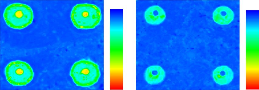
NATURE COMMUNICATIONS | https://doi.org/10.1038/s41467-020-20651-w                                                                      ARTICLE

    a                                                 Zone Ia                                                                              Zone Ib

                                                      5 µm                                                    1.
           PMMA
                                   EBL                                   Na/K
           Graphene
           Si / SiO2                                                                                         2. PhCN
                                                                                                             3. Acetone
                                                                                                             4. PMMA                  EBL

               D        Zone IIIa                    D       Zone IIb                                                                       Zone IIa

               20 µm                EBL                                 1. D2O                                     Na/K            15 µm
                                                                        2. PhCN
                                                                        3. Acetone
                    Na/K                                                4. PMMA
                                                                                                                                   Zone Ib
                                                                      Zone IIIb                                                Zone IIb
               D                             Zone IV D           Cl                                                         Zone IIIb
                                                                                               D       Cl                                 D Cl
                                                                                                                        Zone V
                                  1. ICl                                    Acetone
                                 2. PhCN

    b                                                                                                               c
                                                                                                                                  D      Cl

                                                                                                                                  . . .

                                       Graphene embroidery                                                                        X X X X= O, H

Fig. 1 Reaction sequence towards multiply patterned graphene architectures. a Schematic illustration of the reaction sequence for the multiple patterning
functionalization of a graphene monolayer. PMMA: polymethyl methacrylate. EBL: electron-beam lithography; zone Ia, IIa, and IIIa: the step-wise EBL
exposed graphene areas (black circle with diameters of 5 µm, black concentric ring with diameters of 15 µm, and 20 µm) before functionalization; zone Ib,
IIb, and IIIb: reagent-accessible graphene areas after activation/functionalization. The first addend zone (zone Ib), showing covalently bound bromophenyl
units, is indicated in red; the second addend zone (zone IIb), covalently bound deutero-atoms, is indicated in blue; the third addend zone (zone IIIb),
covalently bound chloro-atoms, is indicated in orange. Zone IV: PMMA-covered graphene and zone V: intact monolayer graphene after final PMMA
removal. Each patterning process includes first spin-coating of a PMMA double-layer mask, and then EBL-based patterning of the graphene–PMMA
assembly. The subsequent 2D-functionalization comprises: (1) addition of the trapping electrophile including 4-bromobenzene diazonium-
tetrafluoroborate, deuteroxide, and iodine monochloride to graphene area reductively activated by sodium/potassium (Na/K) alloy; (2) quenching the
reaction and the removal of residual charges by the addition of benzonitrile (PhCN);26 (3) washing with acetone to remove unreacted chemicals as well as
the old PMMA coverage. As this reagent leads to a partial degradation of the protective PMMA layer, the old PMMA coverage is removed by acetone. By
this procedure, the initially created addend patterns (zone Ib, zone IIb) become covered by PMMA, but can be retrieved by the aid of a lithographically
applied crosshair pattern, for details see supplementary section S2; and (4) re-spin-coating of a fresh PMMA layer. b Example image of the resulting
graphene embroidery via molecular embroidering strategy. c During the entire reaction procedures, strain-free antaratopic additions provided by surface
atoms (i.e., O) of the underlying Si/SiO2 substrate were enabled. Inert substrates would allow only for successive supratopic additions, which however are
forbidden due to the enormous amount of strain energy that would be built up27.

patterning of graphene with different addends bound to spatially                  the constructed 2D-hetero-architecture can be tailored. Regular
defined addend zones. The concept can be considered as a                           patterns of hydrogen/deuteration-covered regions result in a
molecular embroidery analogy to the traditional embroidery                        confinement potential for the carriers in the pristine graphene
manufacturing, that is, employing spatially resolved graphene                     regions, thus leading to a bandgap opening and characteristic for
chemistry (needle) to embroider regularly patterned addend                        a n-type semiconductor3. The bandgap depends on the amount of
zones to graphene (fabric). With this pioneering concept various                  attached hydrogen/deuterium atoms. On the other hand
2D-patterns beyond this concentric pattern can easily be                          chlorination causes p-doping36. By the attachment of differently
accomplished by a tailor-made modification of the respective e-                    substituted aromatic substituents (σ/π-donor or acceptor) a
beam lithographic masks.                                                          specific geometrically defined region of the graphene lattice can
  For our multiply patterned graphene, where the different                        be addressed directly (here is aromatic acceptor) and fine-tuned
functionalities including deuterium, chlorine, and bromobenzene                   with respect to its electrical properties. As a consequence, our
were selectively bound to the graphene surface, the properties of                 constructed multiply patterned graphene with concentric

NATURE COMMUNICATIONS | (2021)12:552 | https://doi.org/10.1038/s41467-020-20651-w | www.nature.com/naturecommunications                                 3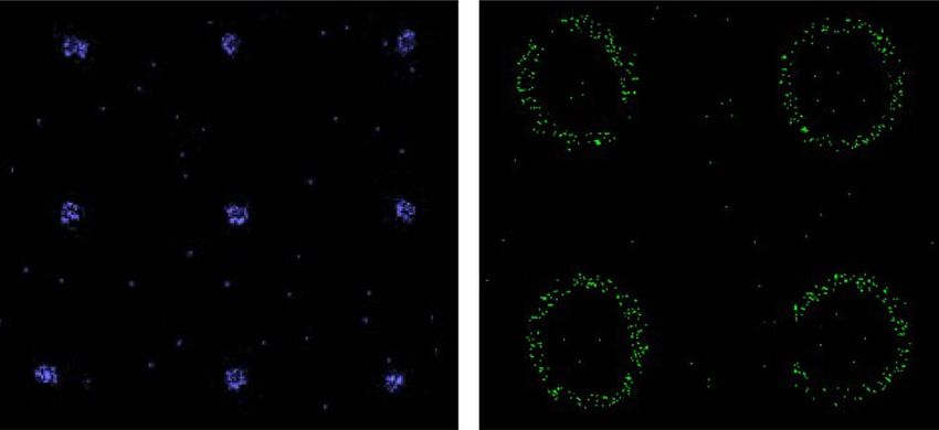
ARTICLE                                                                                                          NATURE COMMUNICATIONS | https://doi.org/10.1038/s41467-020-20651-w

             a                                                                                                         b

             Normalized Raman G Band Intensity / a.u.

                                                                                                                        Normalized Raman G Band Intensity / a.u.
                                                                               Zone Ia
                                                                                                                                                                                     Zone IIa

                                                                               Zone V
                                                                                                                                                                                     Zone V

                                                                               Zone Ib                                                                                               Zone IIb

                 1000                                             1500    2000        2500                 3000             1000                                          1500    2000         2500         3000
                                                                     Raman shift / cm-1                                                                                      Raman shift / cm -1

                c                                                                                                          d
               Normalized Raman G Band Intensity / a.u.

                                                                                                                                                                                                      Zone V

                                                                                                                                    Normalized Frequency / a.u.
                                                                                                                                                                                                      Zone Ib
                                                                                 Zone IIIa                                                                                                            Zone IIb
                                                                                                                                                                                                      Zone IIIb

                                                                                 Zone V

                                                                                 Zone IIIb

                   1000                                           1500    2000        2500                 3000                                                    0.0   0.5   1.0     1.5     2.0    2.5     3.0
                                                                                                                                                                                     ID / IG
                                                                     Raman shift / cm-1
Fig. 2 Statistical Raman analysis of a multiply patterned graphene monolayer. a Raman spectra of zone Ia (before arylation), zone V (after arylation and
PMMA removal) and zone Ib (after arylation). b Raman spectra of zone IIa (before deuteration), zone V (after deuteration and PMMA removal) and zone
IIb (after deuteration). c Raman spectra of zone IIIa (before chlorination), zone V (after chlorination and PMMA removal) and zone IIIb (after chlorination).
d Statistical Raman histograms of ID/IG ratio extracted from Raman spectra of: (a) zone Ib (blue), (b) zone IIb (cyan), (c) zone IIIb (green), and (d) zone V
(black). ID/IG: Raman D-band to G-band intensity ratio. Averaged spectra (∼200 single point spectra) of the respective zones, λexc = 532 nm.

patterns, where each patterned graphene nanodomain has distinct                                                        attached chromophore) in different areas on the same electrical
semi-conducting behavior (n-type and p-type), bears promising                                                          conducting substrate. Thus, it may also find applications in
potential to form graphene p–n junctions. Furthermore, the                                                             nanometer scale optoelectronics such as light sensor. Finally, our
properties of these type of chemically written p–n junctions may                                                       innovative approach of writing chemical information into
further be fine-tuned by the control of the degree of functiona-                                                        spatially defined patterns may also become of great importance
lization in each addend zone (for details see section Thermal                                                          in a field of information storage based on distinct chemical
stability and reversibility). Semiconductor p–n junctions are                                                          molecules where more than only two states (on/off, which is the
elementary building blocks for many electronic devices such as                                                         typical two-state electrical process of traditional information
transistors, solar cells, photodetectors, and integrated circuits and                                                  storage) of information can be stored.
the potential applications of our constructed graphene p–n
junctions in these fields can be reasonably expected. Besides, these                                                    Statistical Raman analysis. For the characterization of the con-
constructed p–n junctions are always combined with the electric                                                        centrically patterned graphene sheets we applied SRS. The mean
conductivity of the surround intact graphene regions (zone V),                                                         Raman spectra of the patterned zones are shown in Fig. 2. The
whose geometry can be tailored on demand upon the strategy that                                                        zone Ia (before functionalization) shows a pronounced G-band at
we introduce here. In view of this, the blueprint for promising all-                                                   1582 cm−1 indicative for a sp2 carbon lattice along with a negli-
graphene nanoscale electronic circuits is laid. Moreover, con-                                                         gible defect-induced D-band at 1350 cm−1. This is the char-
sidering the fact that some aromatic systems are sensitive to light,                                                   acteristic feature of an intact monolayer graphene. The absence of
the 2D-architectures we constructed can write phenyl-based                                                             a D-band demonstrates that during the EBL process no defects in
substituents to distinct areas on the graphene flake, resulting in                                                      the graphene lattice were generated. After the reductive arylation
harvesting light of different wavelengths (based on the type of                                                        a very intense D-band emerged, demonstrating the efficient

4                                                         NATURE COMMUNICATIONS | (2021)12:552 | https://doi.org/10.1038/s41467-020-20651-w | www.nature.com/naturecommunications
NATURE COMMUNICATIONS | https://doi.org/10.1038/s41467-020-20651-w ARTICLE
a b c
d e f
ID /IG
0.0
0.4
0.8
1.2
1.6
2.0
2.4
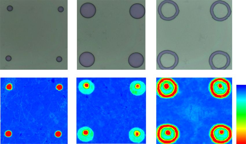
Fig. 3 Optical images of pattern and large-scale Raman ID/IG mapping. a, b, c Optical image of PMMA (polymethyl methacrylate) patterned graphene
(precursor masks) for each step. The purple areas are the exposed graphene regions and the light green areas are covered by PMMA. d, e, f The
corresponding Raman ID/IG mapping images after addend binding and removal of the PMMA layer. ID/IG: Raman D-band to G-band intensity ratio. The
variations in color from blue to red in (d, e, f) represent the change in ID/IG ratio from 0 to 2.4. The red circles (exposed regions, zone Ib) and blue
background (covered regions, zone V) in (d) denote the ID/IG ratios are 2.4 and 0, respectively. The red circles (zone Ib), turquoise concentric rings (zone
IIb), and blue background (zone V) in (e) denote ID/IG ratios are 2.4, 0.7, and 0, respectively. The red circles (zone Ib), turquoise concentric rings (zone IIb),
red concentric rings (zone IIIb), and blue background (zone V) denote ID/IG ratios are 2.4, 0.7, 2.4, and 0, respectively. Scale bar = 5 µm.
conversion of sp2 into sp3 carbon atoms within the corresponding system within zone IIb as manifested by a downshift of the Raman
carbon lattice of zone Ib. The ID/IG (Raman D-band to G-band G-band to 1567 cm−1 (the G-band locates at 1582 cm−1 before
intensity ratio) ratio raised fromARTICLE NATURE COMMUNICATIONS | https://doi.org/10.1038/s41467-020-20651-w
Fig. 4 Temperature-dependent Raman analyses. Temperature-dependent statistical Raman spectra of: a zone Ib, b zone IIb, and c zone IIIb. d Mean Raman
ID/IG ratio extracted from the temperature-dependent Raman spectra of (a, b, c). Raman ID/IG mapping after: e 250 °C annealing and f 400 °C annealing.
The variations in color from blue to red in (e) and (f) represent the change in ID/IG ratio from 0 to 2.4. The yellow circles, turquoise concentric rings, green
concentric rings, and blue background in (e) denote ID/IG ratios are 1.8, 0.7,1, and 0, respectively. The turquoise hollow rings and blue background in (f)
denote ID/IG ratios are 1 and 0, respectively. ID/IG: Raman D-band to G-band intensity ratio. Scale bar = 5 µm.
a b 200 °C for zone IIIb and at 250 °C for zone Ib. The experimentally
observed different thermal stabilities for zone Ib (C–C bond
cleavage), zone IIb (C–D bond cleavage), and zone IIIb (C–Cl
bond cleavage) correlate very well with the corresponding bond
strengths (BE (C–Cl) = 328 kJ mol−1, BE (C–C) = 332 kJ mol−1,
and BE (C–D) = 414 kJ mol−1)40–44.
As mentioned above, the reversible defunctionalization process
mainly occurs in the temperature range between 200 and 350 °C
for zone Ib and IIIb. Therefore, for instance, upon heating to
250 °C, we can tune the ID/IG ratio of zone Ib and zone IIIb to
Br Cl around 1.8 and 1, respectively. The large-scale Raman mapping
clearly displayed the pattern image with the corresponding
Fig. 5 SEM-EDS analyses. a EDS elemental mapping of bromine (Br, blue decreased ID/IG ratios, respectively, encoded in yellow for zone Ib
circles). b EDS elemental mapping of chlorine (Cl, green concentric rings). and green for zone IIIb (Fig. 4e). The 400 °C heating treatment
SEM-EDS: Scanning electron microscopy/energy dispersive X-ray resulted in the complete defunctionalization of both zone Ib
spectroscopy. Scale bar = 5 µm. and IIIb and leave only zone IIb intact, which is confirmed by
large-scale Raman mapping that the corresponding pattern image
up to 500 °C, indicating a very high thermal stability (Fig. 4b). changes from the previous concentric circle to the hollow circle
Further increasing the temperature to 600 °C causes the complete (Fig. 4f). Taking into account that the electronic character of
loss of all Raman features including the G- and 2D-bands and the the remaining conjugated π-system within a functionalized zone
establishment of a flat line. This demonstrates the complete depends on the extent of functionalization such as chlorination,
destruction of the graphene framework rather than just the this reversible defunctionalization process enables the adjustment
cleavage of C–D bonds. Similar to zone Ib, the temperature- of the electronic properties (band gap engineering).
correlated D-band alteration was also found in zone IIIb and the The defunctionalization behavior of this 2D-hetero-
D-band decreases continuously with increasing temperature architectures also can be triggered by a re-reduction treatment
(Fig. 4c). The decline of the D-band is a result of the C–Cl bond with Na/K alloy (Supplementary section S6) and the different
cleavage accompanied by sp3 to sp2 rehybridization. A closer look addend zones (Ib, IIb, and IIIb) exhibit different defunctionaliza-
at the addend cleavage as a function of temperature nicely reflects tion processes (Supplementary Figs. 8–10). For zones Ib and IIIb,
the different thermal stabilities of zones Ib and IIIb. For the as the reduction time increases, the Raman D-band decreases
chlorinated zone IIIb, the Raman features approaches that of continuously, which is indicative of an ongoing defunctionaliza-
pristine graphene at 300 °C instead of 350 °C, observed for the tion reaction. After 4 and 3 h of reductive treatment, respectively,
arylated zone Ib. Besides, the main addend cleavage sets in at the D-band of zone Ib and zone IIIb have almost vanished,
6 NATURE COMMUNICATIONS | (2021)12:552 | https://doi.org/10.1038/s41467-020-20651-w | www.nature.com/naturecommunicationsNATURE COMMUNICATIONS | https://doi.org/10.1038/s41467-020-20651-w ARTICLE
suggesting a reversible defunctionalization processes. This is in Spec 5. The temperature-dependent Raman measurements were performed in a
clear line with similar studies carried out for carbon nanotubes45, Linkam stage THMS 600, equipped with a liquid nitrogen pump MS94 for tem-
perature stabilization under a constant flow of nitrogen. Nitrogen gas needs to be
bulk graphene46, and C60 derivatives47,48 and a clear indication filled for 20 min before starting the measurements to remove air. The measure-
that also in monolayer graphene systems, a post-functionalization ments were carried out on Si/SiO2 wafers with a heating rate of 10 K min−1.
reduction leads to a detachment of the previously introduced
covalent functionalities. However, a completely different behavior SEM-EDS. SEM-EDS was performed on a GeminiSEM 500 equipped with Oxford
was observed for deuterated graphene within zone IIb (Supple- X-max 150. The working conditions were set at an operating at accelerating voltage
mentary Fig. 10). After 4 h and even up to 24 h of re-reduction of 5 kV, working distance of 7.3 mm, the elevation angle of detector is 35°, and the
sample is vertical to the secondary-electron emission.
treatment, the corresponding Raman D-band remains unchanged
(Supplementary Fig. 11 and Supplementary Table 3), indicative
for its high stability. These results are in line with the thermal Data availability
The authors declare that the data supporting the findings of this study are available
treatment investigations.
within the article and its Supplementary Information files. All other relevant data
supporting the findings of this study are available from the corresponding author on
SEM-EDS analyses. To track the chemical nature of this multiply request.
patterned graphene, we carried out SEM-EDS (Fig. 5). Our pat-
terned graphene containing the three addend zones Ib–IIIb con- Received: 17 April 2020; Accepted: 11 December 2020;
tains the SEM-EDS detectable elements Br (zone Ib) and Cl (zone
IIIb). As expected, SEM-EDS investigation of the Br distribution
in zone Ib revealed periodic solid circular dot configurations
correlating very well with the extension of zone Ib. When it comes
to the element Cl, a distribution related to zone IIIb, namely, a References
periodic ring configuration, is observed. The SEM-EDS results 1. Bai, J. W., Zhong, X., Jiang, S., Huang, Y. & Duan, X. F. Graphene nanomesh.
strongly correlate with the Raman data outlined above. In addi- Nat. Nanotechnol. 5, 190–194 (2010).
tion, the Br and Cl atoms are quite homogeneously distributed 2. Li, X. L., Wang, X. R., Zhang, L., Lee, S. W. & Dai, H. J. Chemically derived,
ultrasmooth graphene nanoribbon semiconductors. Science 29, 1229–1232
with the corresponding addend zones Ib and IIIb, demonstrating a
(2008).
homogeneous addend coverage. Moreover, no further element 3. Balog, R. et al. Bandgap opening in graphene induced by patterned hydrogen
signals are found, which indicates the efficiency of all washing adsorption. Nat. Mater. 9, 315–319 (2010).
and work-up procedures and underlines the covalent nature of 4. Elias, D. C. et al. Control of graphene’s properties by reversible hydrogenation:
the patterned regions evidence for graphane. Science 323, 610–613 (2009).
5. Bai, J., Duan, X. & Huang, Y. Rational fabrication of graphene nanoribbons
using a nanowire etch mask. Nano Lett. 9, 2083–2087 (2009).
Discussion 6. Wang, X. & Dai, H. Etching and narrowing of graphene from the edges. Nat.
In summary, we have realized the first prototype of multiply Chem. 2, 661–665 (2010).
functionalized and hierarchically patterned graphene sheets with 7. George, A. et al. Large area resist-free soft lithographic patterning of graphene.
Small 9, 711–715 (2013).
a spatially defined 2D-hetereo-architecture. The chemical 8. Zhang, L. M. et al. Photocatalytic patterning and modification of graphene. J.
embroidery was accomplished by repetitive EBL/reduction/ Am. Chem. Soc. 133, 2706–2713 (2011).
antaratopic-covalent-binding sequences starting with PMMA- 9. Abbas, A. N. et al. Patterning, characterization, and chemical sensing
covered graphene deposited on a Si/SiO2 substrate. The corre- applications of graphene nanoribbon arrays down to 5 nm using helium ion
sponding functionalization zones carry bromobenzene-, deutero-, beam lithography. ACS Nano 8, 1538–1546 (2014).
10. Hyun, W. J., Secor, E. B., Hersam, M. C., Frisbie, C. D. & Francis, L. F. High-
and chloro-addends. The successful covalent patterning was resolution patterning of graphene by screen printing with a silicon stencil for
unequivocally demonstrated by SRS and SEM-EDS. In addition, highly flexible printed electronics. Adv. Mater. 27, 109–115 (2015).
the constructed concentric hetero-architectures were very clearly 11. Cai, J. et al. Atomically precise bottom-up fabrication of graphene
visualized by large-scale Raman ID/IG mapping. Moreover, the nanoribbons. Nature 466, 470–473 (2010).
different thermal stabilities for each addend zone were revealed 12. Narita, A. et al. Synthesis of structurally well-defined and liquid phase-
processable graphene nanoribbons. Nat. Chem. 6, 126–132 (2014).
by temperature-dependent Raman investigations and the rever- 13. Dössel, L., Gherghel, L., Feng, X. & Müllen, K. Graphene nanoribbons by
sibility of the covalent binding, as seen for the chloro- and bro- chemists: nanometer-sized, soluble, and defect-free. Angew. Chem. Int. Ed. 50,
mobenzene-functionalities, provide a feasible means for property 2540–2543 (2011).
engineering (e.g., electronic structure). The construction principle 14. Schwab, M. G. et al. Structurally defined graphene nanoribbons with high
of 2D-patterning that we have introduced here opens enormous lateral extension. J. Am. Chem. Soc. 134, 18169–18172 (2012).
15. Narita, A., Feng, X. L. & Müllen, K. Bottom-up synthesis of chemically precise
opportunities towards tailoring the physical and chemical prop- graphene nanoribbons. Chem. Rec. 15, 295–309 (2015).
erties of graphene sheets with apparently limitless combinations 16. Koehler, F. M. et al. Permanent pattern-resolved adjustment of the surface
of spatially defined surface functionalities. Such tailored nano- potential of graphene-like carbon through chemical functionalization. Angew.
surfaces are highly attractive for high-performance applications, Chem. Int. Ed. 48, 224–227 (2009).
for example, in the fields of optoelectronics, sensors, and catalysis. 17. Sun, Z. Z. et al. Towards hybrid superlattices in graphene. Nat. Commun. 2,
559–564 (2011).
18. Liu, L. H. et al. A simple and scalable route to wafer-size patterned graphene.
Methods J. Mater. Chem. 20, 5041–5504 (2010).
Covalent patterning and reductive functionalization of graphene. The details 19. Bian, S. et al. Covalently patterned graphene surfaces by a force-accelerated
on the multi-step covalent patterning and activation/functionalization of graphene Diels-Alder reaction. J. Am. Chem. Soc. 135, 9240–9243 (2013).
and the involved chemicals are given in the Supplementary Information S2 and S3. 20. Li, J. et al. Click and patterned functionalization of graphene by Diels-Alder
reaction. J. Am. Chem. Soc. 138, 7448–7451 (2016).
21. Ye, D. et al. Patterned graphene functionalization via mask-free scanning of
Raman spectroscopy. The Raman spectroscopic characterization was performed
micro-plasma jet under ambient condition. Appl. Phys. Lett. 104,
on a Horiba Jobin Yvon LabRAM Aramis. The spectrometer was calibrated by
103105–103109 (2014).
using crystalline graphite. All measurements were conducted using a laser
22. Lee, W. K., Whitener, K. E., Robinson, J. J. T. & Sheehan, P. E. Patterning
(Olympus LMPlanFl50x, NA 0.50) with an excitation wavelength of 532 nm, with
magnetic regions in hydrogenated graphene via e-beam irradiation. Adv.
an acquisition time of 2 s. Spectral data were obtained through a motorized x-y
table in a continuous line scan mode (SWIFT-module). The step sizes in the Mater. 27, 1774–1778 (2015).
Raman mappings were kept in the range of 0.1–0.5 µm depending on the experi- 23. Lee, W. H. et al. Selective-area fluorination of graphene with fluoropolymer
ments. The corresponding data processing was performed using software of Lab and laser irradiation. Nano Lett. 12, 2374–2378 (2012).
NATURE COMMUNICATIONS | (2021)12:552 | https://doi.org/10.1038/s41467-020-20651-w | www.nature.com/naturecommunications 7ARTICLE NATURE COMMUNICATIONS | https://doi.org/10.1038/s41467-020-20651-w
24. Wei, T. et al. Highly efficient and reversible covalent patterning of graphene: 48. Moonen, N.N.P. et al. The chemical retro-Bingel reaction: selective removal of
2D-management of chemical information. Angew. Chem. Int. Ed. 59, bis(alkoxycarbonyl)methano addends from C60 and C70 with amalgamated
5602–5606 (2020). magnesium.Chem. Commun. 36, 335–336 (2000).
25. Bao, L. P. et al. Spatially resolved bottom-side fluorination of graphene by 2D-
substrate patterning. Angew. Chem. Int. Ed. 59, 6766–6771 (2020).
26. Vecera, P. et al. Solvent-driven electron trapping and mass transport in Acknowledgements
reduced graphites to access perfect graphene. Nat. Commun. 7, 12411–12418 This work was financially supported by Deutsche Forschungsgemeinschaft (DFG, Ger-
(2016). man Research Foundation) – Project number 182849149 – SFB 953.
27. Schäfer, R. A. et al. Substrate-modulated reductive graphene functionalization.
Angew. Chem. Int. Ed. 55, 14858–14862 (2016). Author contributions
28. Wang, Q. H. et al. Understanding and controlling the substrate effect on A.H. and T.W. conceived the research, designed the experiments and co-wrote the paper.
graphene electron-transfer chemistry via reactivity imprint lithography. Nat. A.H. and F.H. supervised the project as scientific group leader and principal investigator.
Chem. 4, 724–732 (2012). T.W. synthesized the samples, performed Raman spectroscopy, SEM/EDS measurement
29. Amsharov, K. et al. Fractal-seaweeds type functionalization of graphene. and analyzed the data. M.K. and H.B.W. prepared the patterns on graphene. All the
Carbon 158, 435–448 (2020). authors discussed the results and contributed to writing the manuscript.
30. He, P. L. et al. Capillary electrophoresis of covalently functionalized single-
chirality carbon nanotubes. Electrophoresis 38, 1669–1677 (2017).
31. Peng, Z. W. et al. Graphene as a functional layer for semiconducting carbon Funding
nanotube transistor sensors. Carbon 125, 49–55 (2017). Open Access funding enabled and organized by Projekt DEAL.
32. Mazza, A. R. Atomic deuteration of epitaxial many-layer graphene on 4H-SiC
(0001−). J. Vac. Sci. Technol. B 37, 0418041–0418046 (2019).
33. Schäfer, R. A. et al. On the way to graphane—pronounced fluorescence of
Competing interests
The authors declare no competing interests.
polyhydrogenated graphene. Angew. Chem. Int. Ed. 52, 754–757 (2013).
34. Li, B. et al. Photochemical chlorination of graphene. ACS Nano 5, 5957–5961
(2011). Additional information
35. Wu, J. et al. Controlled chlorine plasma reaction for noninvasive graphene Supplementary information is available for this paper at https://doi.org/10.1038/s41467-
doping. J. Am. Chem. Soc. 133, 19668–19671 (2011). 020-20651-w.
36. Zhang, X. et al. Impact of chlorine functionalization high-mobility chemical
vapor deposition grown graphene. ACS Nano 7, 7262–7270 (2013). Correspondence and requests for materials should be addressed to A.H.
37. Dong, X. C. et al. Doping single-layer graphene with aromatic molecules.
Small 5, 1422–1426 (2009). Peer review information Nature Communications thanks M. Angeles Herranz, and the
38. Das, B., Voggu, R., Rout, C. S. & Rao, C. N. R. Changes in the electronic other, anonymous, reviewer(s) for their contribution to the peer review of this work. Peer
structure and properties of graphene induced by molecular charge-transfer. reviewer reports are available.
Chem. Commun. 5155–5157 (2008).
39. Cançado, L. G. et al. Quantifying defects in graphene via Raman spectroscopy Reprints and permission information is available at http://www.nature.com/reprints
at different excitation energies. Nano Lett. 11, 3190–3196 (2011).
40. Paris, A. et al. Kinetic isotope effect in the hydrogenation and deuteration of Publisher’s note Springer Nature remains neutral with regard to jurisdictional claims in
graphene. Adv. Funct. Mater. 23, 1628–1635 (2013). published maps and institutional affiliations.
41. Sinitskii, A. et al. Kinetics of diazonium functionalization of chemically
converted graphene nanoribbons. ACS Nano 4, 1949–1954 (2010).
42. Ijäs, M. & Harju, A. Fracturing graphene by chlorination: a theoretical
Open Access This article is licensed under a Creative Commons
viewpoint. Phys. Rev. B 85, 035440–035450 (2012).
Attribution 4.0 International License, which permits use, sharing,
43. Liu, X. Y., Zhang, J. M. & Xu, K. W. Chlorine molecule adsorbed on
adaptation, distribution and reproduction in any medium or format, as long as you give
graphene and doped graphene: a first-principle study. Phys. B 436, 54–58
appropriate credit to the original author(s) and the source, provide a link to the Creative
(2014).
44. Pykal, M., Jurečka, P., Karlický, F. & Otyepka, M. Modelling of graphene Commons license, and indicate if changes were made. The images or other third party
functionalization. Phys. Chem. Chem. Phys. 18, 6351–6372 (2016). material in this article are included in the article’s Creative Commons license, unless
45. Syrgiannis, Z. et al. Reductive retrofunctionalization of single-walled carbon indicated otherwise in a credit line to the material. If material is not included in the
nanotubes. Angew. Chem. Int. Ed. 49, 3322–3325 (2010). article’s Creative Commons license and your intended use is not permitted by statutory
46. Knirsch, K. C. et al. Mono- and ditopic bisfunctionalization of graphene. regulation or exceeds the permitted use, you will need to obtain permission directly from
Angew. Chem. Int. Ed. 55, 5861–5864 (2016). the copyright holder. To view a copy of this license, visit http://creativecommons.org/
47. Kessinger, R. et al. Preparation of enantiomerically pure C76 with a general licenses/by/4.0/.
electrochemical method for the removal of di(alkoxycarbonyl)methano
bridges from methanofullerenes: the retro-Bingel reaction. Angew. Chem. Int.
© The Author(s) 2021
Ed. 37, 1919–1922 (1998).
8 NATURE COMMUNICATIONS | (2021)12:552 | https://doi.org/10.1038/s41467-020-20651-w | www.nature.com/naturecommunicationsYou can also read