How antisolvent miscibility affects perovskite film wrinkling and photovoltaic properties
←
→
Page content transcription
If your browser does not render page correctly, please read the page content below
ARTICLE
                  https://doi.org/10.1038/s41467-021-21803-2                 OPEN

                  How antisolvent miscibility affects perovskite film
                  wrinkling and photovoltaic properties
                  Seul-Gi Kim1, Jeong-Hyeon Kim1, Philipp Ramming2,3, Yu Zhong2,3, Konstantin Schötz3, Seok Joon Kwon1,4,
                  Sven Huettner 2, Fabian Panzer 3 & Nam-Gyu Park 1 ✉
1234567890():,;

                  Charge carriers’ density, their lifetime, mobility, and the existence of trap states are strongly
                  affected by the microscopic morphologies of perovskite films, and have a direct influence on
                  the photovoltaic performance. Here, we report on micro-wrinkled perovskite layers to
                  enhance photocarrier transport performances. By utilizing temperature-dependent miscibility
                  of dimethyl sulfoxide with diethyl ether, the geometry of the microscopic wrinkles of the
                  perovskite films are controlled. Wrinkling is pronounced as temperature of diethyl ether (TDE)
                  decreases due to the compressive stress relaxation of the thin rigid film-capped viscoelastic
                  layer. Time-correlated single-photon counting reveals longer carrier lifetime at the hill sites
                  than at the valley sites. The wrinkled morphology formed at TDE = 5 °C shows higher power
                  conversion efficiency (PCE) and better stability than the flat one formed at TDE = 30 °C.
                  Interfacial and additive engineering improve further PCE to 23.02%. This study provides
                  important insight into correlation between lattice strain and carrier properties in perovskite
                  photovoltaics.

                  1 School
                         of Chemical Engineering, Sungkyunkwan University (SKKU), Suwon, Korea. 2 Department of Chemistry, University of Bayreuth, Bayreuth, Germany.
                  3 Chair
                        for Soft Matter Optoelectronics, University of Bayreuth, Bayreuth, Germany. 4 Nanophotonics Research Center, Korea Institute of Science and
                  Technology (KIST), Seoul, Korea. ✉email: npark@skku.edu

                  NATURE COMMUNICATIONS | (2021)12:1554 | https://doi.org/10.1038/s41467-021-21803-2 | www.nature.com/naturecommunications                         1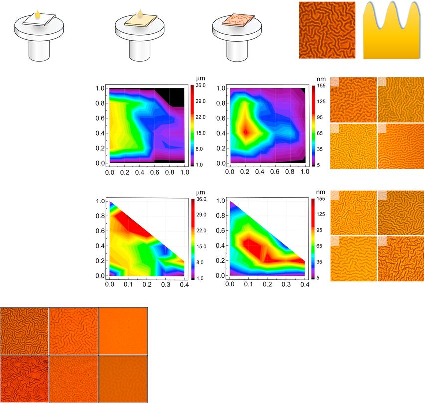
ARTICLE NATURE COMMUNICATIONS | https://doi.org/10.1038/s41467-021-21803-2
S
ince the pioneering reports on the ~10% efficient solid-state represented as a sinusoidal curve with a wavelength (λ) and an
perovskite solar cell (PSC) in 20121,2, demonstrating long- amplitude (A). λ is estimated by calculating the governing char-
term stability by resolving the dissolution issue of acteristic periodic length scales from the 2D Fourier transform of
organic–inorganic lead halide perovskite in photoelectrocehmical- optical microscope images (Supplementary Fig. 1) and A by cal-
type solar cell employing liquid electrolyte3,4, the perovskite culating the average height difference between the hill (hhill) and
photovoltaics has surged swiftly. As a result, the power conversion the valley (hvalley) such that A = (hhill − hvalley)/2. From the
efficiency (PCE) as high as 25.5% has been achieved in 20205. experiments, we found that the wrinkling geometry is affected by
Although the composition of perovskite started with methy- substrate temperature (TSub) and the temperature of diethyl ether
lammonium lead iodide, abbreviated to MAPbI3, the recent (TDE), as well as the perovskite composition. For example, the
excellent performing PSCs are based on formamidinium lead wrinkle geometry exhibited a dependence on the compositions of
iodide, abbreviated to FAPbI36–8 or its derivatives with a certain FAPbI3 perovskite. Hereby MA (or Cs) and Br are used as a
amount of other cations in FA-site and/or bromide in I site9–11. substitute for FA and I in FAPbI3 to form nominal compositions
Along with compositional engineering for making progress of FA1–xMAxPb(BryI1–y)3 and FA1–zCszPb(BryI1–y)3, and MA and I
toward higher PCE, methods for controlling crystal growth have are partially substituted with Cs and Br in MAPbI3, leading to
significantly contributed to producing defect-less high-quality MA1–wCswPb(BryI1–y)3. Figure 1b, c show detailed phase diagram
perovskite films12,13. Forming Lewis acid–base adduct inter- of the wrinkle geometries as a function of the composition para-
mediate via antisolvent engineering was widely adapted to achieve meters (i.e., x and y for Fig. 1b and z and y for Fig. 1c, respectively)
large perovskite crystals with less grain boundaries14,15, instead of (see Supplementary Fig. 1a, b for entire experimental data for the
a direct conversion of wet film to the perovskite phase. Despite the wrinkled morphologies). We observed that the wrinkling occurs in
enlarged perovskite grains, the crystal growth by solvent engi- selective range of the compositions (i.e., 0 ≤ x ≤ 0.4 and 0.2 ≤ y ≤
neering can hardly manipulate morphology of perovskite layer. 0.8) or (0.6 ≤ x ≤ 0.8 and 0.4 ≤ y ≤ 0.6) in FA1–xMAxPb(BryI1–y)3
Epitaxial growth, for example, could provide crystal growth nor- and (z = 0.1 and 0 ≤ y ≤ 0.8), (z = 0.2 and 0 ≤ y ≤ 0.6), (z = 0.3 and
mal to the substrate, which is expected to be beneficial to carrier 0.2 ≤ y ≤ 0.4) or (z = 0.4 and y = 0.2) in FA1–zCszPb(BryI1–y)3)
transport. In addition, a flat perovskite surface induced by the Notably, we also observe that there is no wrinkling in MAPbI3 or
solvent engineering may not be effective in optimizing light in- its derivatives (see Supplementary Fig. 1c, d). In addition, hundred
and out-coupling. Thus, it is still required to develop a metho- percent Br (FA1–xMAxPbBr3) would not lead to wrinkling (i.e., for
dology enabling an opto-electronically optimized perovskite layer. the FA1–xMAxPb(BryI1–y)3 perovskite, λ tends to increase with
Recently, an approach to control the perovskite morphology decreasing x (Fig. 1b)). From these experimental observations, it is
has been explored. For example, microscopic wrinkles have been obvious that the presence of limited amount of Br plays an
observed for a certain composition of perovskite that suffers important role in introducing the wrinkled morphology. With a
buckling of the perovskite thin film16,17. In particular, the composition of Br in the range of 0.2 ≤ y ≤ 0.8, λ decreases with
buckling was explained as a result of local compressive stress increasing the composition of MA (i.e., λ~20 μm for 0 ≤ x ≤ 0.2,
relaxation17. However, detailed and comprehensive studies for λ~15 μm for 0.2 ≤ x ≤ 0.4, and λ~8 μm for x ≈ 0.6). It is also
effects of the microscopic wrinkles on the photovoltaic perfor- notable that wrinkling hardly occurs for higher composition of x
mances, as well as wrinkling mechanism have not been reported and y such that being >0.8. We also observe that A is relatively
yet. Here, we report a simple and yet effective experimental shallow (~65 nm) for the composition range with 0 ≤ x ≤ 0.4 and
approach to control and optimize the microscopic geometry of 0.2 ≤ y ≤ 0.8, while is deep (~100 nm) for the composition range
the wrinkles of perovskite thin films to maximize the photovoltaic with 0.1 ≤ x ≤ 0.3 and 0.3 ≤ y ≤ 0.6. As shown in Fig. 1c, sub-
performances, as well as long-time durability. We also suggest a stitution of FA with Cs, the wrinkled morphology is accompanied
theoretical model elucidating the wrinkling mechanism based on by further amplified value of A ( > 100 nm) in the range of 0.05 ≤
the detailed experimental data. To control the wrinkled mor- z ≤ 0.4 and 0.2 ≤ y ≤ 0.6. The sampled composition can be
phology, we have designed an experimental method based on expressed as (FAPbI3)1–z(CsPbBr3)z in case of z = y and more
temperature-dependent miscibility of dimethyl sulfoxide (DMSO) detailed phase diagram and images of the wrinkled morphology
with diethyl ether (DE) and composition optimization of per- are provided in Supplementary Fig. 2a, b, and d. Interestingly, the
ovskite materials (i.e., FA1–xMAxPb(BryI1–y)3, FA1-zCszPb(BryI1–y)3 as-spun films prior to the annealing also show a wrinkled mor-
and MA1–wCswPb(BryI1–y)3). To study the detailed mechanism of phology in the range of 0.1 ≤ z ≤ 0.2 (Supplementary Fig. 2a),
the wrinkling, we suggest a bilayer wrinkling model with a the- which is sustained even after the annealing (Supplementary
oretical analysis supported by numerical simulations and Fig. 2b), with slightly decrease in λ (Supplementary Fig. 2d). This
experimental measurement of optical diffraction. We extend a indicates that the solvent evaporation during the annealing pro-
scope of the study to the investigation of the effects of the cess hardly affects the wrinkle framework, as is the context in the
microscopic wrinkles on the charge carrier dynamics with time- case of (FAPbI3)1–x(MAPbBr3)x in Supplementary Fig. 2c, e. The
correlated single-photon counting (TCSPC) coupled with fluor- annealed films show a decrease in the value of λ from 19.7 to
escence lifetime imaging microscopy (FLIM) and photo- 13.9 μm when increasing z from 0.1 to 0.2, while an increase in the
conductive atomic force microscope (pc-AFM). From the value of A from 46.5 nm (z = 0.1) to 112.5 nm (z = 0.2).
combined experimental data, we have found that the wrinkled
morphology notably facilitates the charge carriers transport inside
the perovskite films. Effect of TDE on wrinkled morphologies. Next, with a pre-
sentative sample with the maximum amplitude (i.e., (FAP-
bI3)0.875(CsPbBr3)0.125 (z = 0.125)), we have examined the effects
Results and discussion of TSub and TDE on the wrinkling morphology as shown in
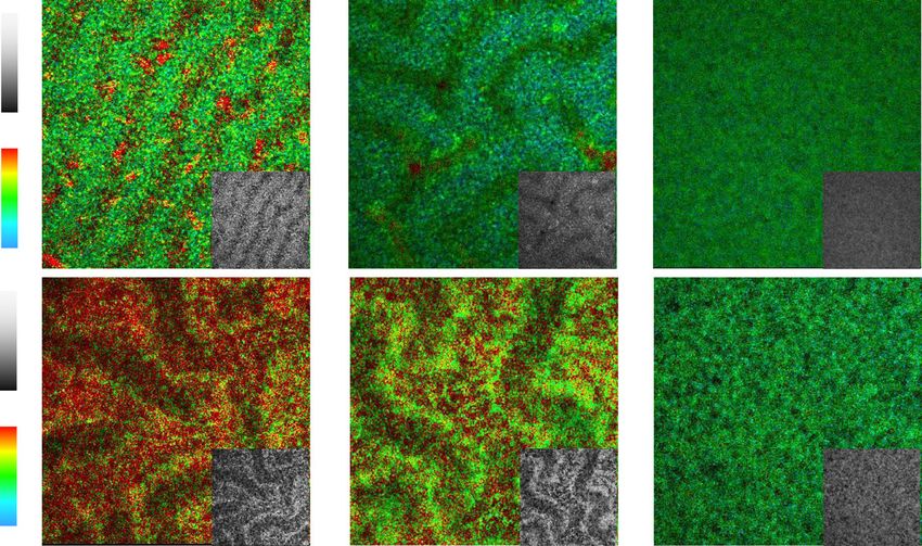
Formation of wrinkled morphologies depending on perovskite Fig. 1d. With fixed TSub, λ decreases and A increases with
composition. Experimental procedure to control microscopic decreasing TDE. The effects of TDE on the wrinkled morphology
wrinkles in PSC is schematically illustrated in Fig. 1a. The per- can be explained by the microscopic phase separation of solvent
ovskite precursor solution is first spin-coated on a solid substrate and antisolvent mixture in which the lower the mixture tem-
for 20 s, followed by dripping DE 10 s right after spinning. The perature the less molar fraction of the solvent, which in turn
cross-sectional profile of the microscopic wrinkles can be shorter wavelength and greater amplitude. Detailed theoretical
2 NATURE COMMUNICATIONS | (2021)12:1554 | https://doi.org/10.1038/s41467-021-21803-2 | www.nature.com/naturecommunications
NATURE COMMUNICATIONS | https://doi.org/10.1038/s41467-021-21803-2                                                                      ARTICLE

Fig. 1 Wrinkled morphologies of perovskite thin film. a A schematic illustration of the experimental procedure to control wrinkled morphology in the
perovskite film, together with an optical microscope image of the wrinkled morphology having amplitude (A) and wavelength (λ). Phase diagrams of the
wrinkled morphology for (b) FA1–xMAxPb(BryI1–y)3 (annealed at 145 °C for 10 min) and (c) FA1–zCszPb(BryI1–y)3 (annealed at 145 °C for 10 min) perovskite
thin films with different compositions. Color maps of wavelength (λ) and amplitude (A) are presented in the middle panels for each composition. Selected
optical microscope images of a1–a4 and b1–b4 are presented in the right panels for each composition. d Optical microscope images for the FA0.875Cs0.125Pb
(Br0.125I0.875)3 perovskite films with different temperatures of TDE and TSub. Scale bar is 50 μm. Dependence of A and λ values on TDEs at a given TSub is
illustrated with bar graph on the right panels.

analysis on the effects of TDE can be found in Supplementary note               and the substrate18. Previous study on the wrinkling of perovskite
1. In addition, there are no wrinkles at sufficiently high TDE such              thin films suggested that the compressive stress can be developed
as 30 °C at a given TSub = 15 °C.                                               by the volume change during a fast perovskite formation by using
                                                                                wafer curvature stress measurements17. This mechanism requires
                                                                                relatively long-time wrinkle formation dynamics up to several
Bilayer model for wrinkling mechanism. The formation of                         minutes to hours19,20. However, we observe that the wrinkles
wrinkling can be explained with a simple thin film mechanics                     form within 10 s. Therefore, we have developed a more detailed
model. In particular, we can employ a bilayer model in which                    model by which the overall morphology of wrinkles can be elu-
wrinkles form in the course of relaxation of a compressive stress               cidated, as well as the wrinkling mechanism based on previous
developed in the perovskite film. It was reported that the com-                  reports17,18. Using a model based on the thin film mechanics, the
pressive stress is due mainly to the differences in the thermal                 wrinkle geometry can be described as a function of the thickness
expansion coefficients between the perovskite precursor solution                 and mechanical constants of the materials. We also derive

NATURE COMMUNICATIONS | (2021)12:1554 | https://doi.org/10.1038/s41467-021-21803-2 | www.nature.com/naturecommunications                               3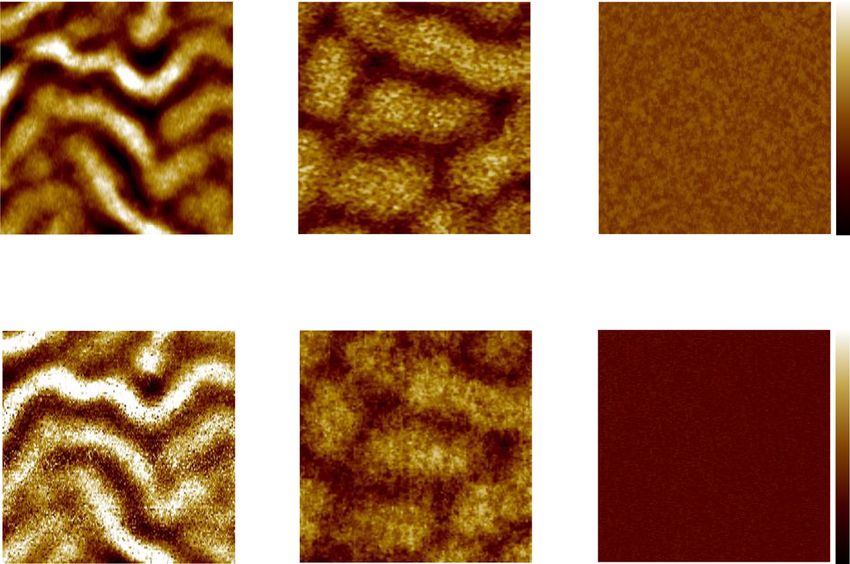
ARTICLE                                                                  NATURE COMMUNICATIONS | https://doi.org/10.1038/s41467-021-21803-2

relationships of λ and A of the wrinkles with the compositions                (samples shown in Supplementary Fig. 5a, b), the viscosity in
and TDE (see detailed analysis in Supplementary note 1).                      the bottom layer indicates that the layer is assuredly different
   To confirm the wrinkling mechanism, in situ photolumines-                   from the top capping layer. Based on the in situ absorption
cence (PL) and simultaneous absorption are examined within the                and emission studies, combined with dynamic viscosity measure-
first 24 s of spinning (see ref. 21. for details of the setup). PL and         ments, we conclude, that the wrinkled structure is likely formed
absorption signals commonly emerge immediately after the                      via a bilayer intermediate with a perovskite top layer on a viscous
contact with DE with duration of spinning of 10 s, indicating                 amorphous bottom layer (case 2 in Fig. 2f), while a flat surface
that perovskite phase forms. As shown in Fig. 2a, the PL peak                 results when not undergoing the bilayer intermediate (case 1 in
initially occurs at 712 nm and then shifts to longer wavelengths              Fig. 2f). Interestingly, too high viscosity (solid precipitate) with
from 10 s to 24 s. A faster change in PL from 712 nm to over                  the composition of z ≥ 0.3 also leads to no wrinkle formation as
760 nm is observed for TDE = 5 and 15 °C, whereas a more                      shown in the Case 3 in Fig. 2f. This indicates that the compressive
gradual change is observed for TDE = 30 °C (Fig. 2b). Extracting              stress of the underlying layer is not dissipated in a local manner,
the band edge evolution from the in situ absorption data (Fig. 2c),           which results in disordered morphological deformation as shown
and comparing it to the corresponding evolution of PL peak                    in the optical microscope image in the Case 3. These findings are
position show, that early after dripping diethyl ether, the PL peak           clearly different from the previous study, suggesting that the
position is at a lower wavelength than the band edge                          crystallization (or nucleation) occurs from the bottom17.
(Supplementary Fig. 3). We interpret this as the optical signature
of a confinement effect, while the subsequent continuous red-shift
of PL and band edge indicates a more Cs and Br rich                           Experimental evidence and numerical simulation for bilayer
stoichiometry at early times followed by more pronounced                      model. To further confirm the bilayer model for the wrinkling
incorporation of FA and I at longer times (see Supplementary                  mechanism, we have numerically simulated the morphological
note 2 for details). We also observe that absorbance becomes                  evolution of the thin film wrinkling based on temporal evolution
stronger at later stage and with increased TDE. This indicates that           of the wrinkle geometry (see details in Supplementary note 3)22.
the growth rate of the thin film thickness (hf) is faster for higher           As shown in Supplementary Figs. 7 and 8, we can find that the
TDE. The absorbance variation dynamics is translated into the                 bilayer model provides qualitatively similar wrinkling morphol-
thin film growth dynamics using the absorption coefficient of the               ogies accompanied by two-dimensional (2D) fast Fourier trans-
perovskite thin films and reference data at equilibrium as shown               form (FFT) images to the experimentally observed images. We
in Fig. 2d demonstrating that the thickness of the perovskite layer           have also tested again the bilayer model by examining the optical
becomes thinner as TDE decreases. (see Supplementary Fig. 3d                  diffraction patterns of the wrinkled thin films (Fig. 2g). As shown
and Supplementary note 2 for detailed procedure). It is also                  in Fig. 2h, the optical diffraction patterns would exhibit different
notable that the PL red-shift is faster for lower TDE (Fig. 2b).              patterns (i.e., concentric ring patterns for the wrinkled bilayer,
   From the in situ PL and absorbance spectra, we can propose                 while dot or single ring pattern for the wrinkled monolayer) with
that the spin-coated perovskite thin film suffers morphological                different configurations as denoted in Fig. 2g. Indeed, we observe
evolution from viscoelastic layer to elastic layer-capped viscoe-             concentric ring patterns at glass side (bottom) of film just after
lastic bilayer. The formation of the elastic capping layer is due             contacted with diethyl ether (10 s after spin started), and the
mainly to the antisolvent, which drives solvents out of the top               patterns disappears with time, whereas the transmitted concentric
part of the coated thin film. In particular, solution of precursor             ring patterns was sustained for long time as shown in Fig. 2i. This
materials of perovskite in DMSO suffers rapid phase separation                can be compared to the diffraction patterns of the wrinkled
by introducing the antisolvent DE at the top surface of the film.              perovskite films obtained from reflected side and transmitted side,
This leads to the fast crystallization of the top region of the spin-         which are commonly sustained over long time (Supplementary
coated layer, which turns into the thin capping layer. The phase              Fig. 9a, b). With the theoretical analysis supported by numerical
separation at lower temperature also gives rise to higher                     calculations and experimental observations of the diffraction
concentration of the perovskite in the top capping layer, which               patterns, we can suggest that the wrinkling of the perovskite thin
can explain the dependences of the wrinkle geometry on TDE (see               films can be elucidated by a bilayer model.
Figs. 1d and 2f, and details in Supplementary note 1with mixing
behavior test in Supplementary Fig. 4). In particular, as shown in            Comparison of photovoltaic property between wrinkled and
Supplementary Fig. 4, we observe higher miscibility at relatively             flat morphology. To study the effect of bilayer-engineered
higher temperatures (i.e., >25.4 °C), while phase separation                  wrinkled perovskite layer to photovoltaic property, current den-
of DMSO and DE mixture at relatively low temperature (i.e.,                   sity(J)–voltage(V) characteristics and external quantum efficiency
NATURE COMMUNICATIONS | https://doi.org/10.1038/s41467-021-21803-2 ARTICLE
a 25 IPL b
175
770 T = 15 oC
PL peak position (nm)
Sub
20 760
200
750
15
Time (s)
740
230 TDE
10 730 5 oC
5
260
720 15 oC
TDE = 5 oC TDE = 15 oC TDE = 30 oC 30 oC
710
0 290
500 600 700 800 500 600 700 800 500 600 700 800 10 12 14 16 18 20 22 24
Wavelength (nm) Wavelength (nm) Wavelength (nm) Time (s)
c 25 O.D. d 500
0 0.000
TSub = 15 oC o
0 C
20 0.1125
=3
400 TDE
Thickness, hf (nm)
0.2250
o
C
= 15
0.3375
Time (s)
15 0.5
0.4500
0.5625
300 TDE
0.6750
0.7875
10 200 TDE = 5 oC
0.9000
1.0 1.013
1.125
5 1.238 100
TDE = 5 oC TDE = 15 oC TDE = 30 oC 1.350
1.462
0 1.5 1.500
0
600 700 800 600 700 800 600 700 800 10 12 14 16 18 20 22 24
Wavelength (nm) Wavelength (nm) Wavelength (nm) Time (s)
e f flat
200 Viscous precipitate Solid or
Case 1 viscous layer
(FAPbI3)1-z(CsPbBr3)z
(FAPbI3)1-z(MAPbBr3)z
Viscosit y (Pa s)
. 150 Z = 0.05
Perovskite Layer hf wrinkle
100 Case 2 Viscous layer H
o
TDE = 15 C Z = 0.15
50 trace
Perovskite Layer hf
Case 3 Solid layer H
0.0 0.1 0.2 0.3 0.4 0.5 0.6 Z = 0.3
Z
g Reflected
patterns i
650 nm 11 s 12 s 14 s 16 s
Laser
Bilayer Monolayer
Transmitted
h patterns
Bilayer Monolayer
Fig. 2 Bilayer-induced wrinkling mechanism. a In situ photoluminescence (PL) measured in the course of spinning from 0 s to 24 s at TSub = 15 °C and
TDE = 5, 15, and 30 °C. b Plot of PL peak positions as a function of spinning time. Spin-coating duration was 20 s (dashed line). c In situ UV–Vis absorption
spectra measured during spinning from 0 s to 24 s at TSub = 15 °C and TDE = 5, 15 °C and 30 °C. d The evolution of the thin solid upper perovskite layer
thickness (hf) calculated from the measured absorption data. Spin-coating duration was 20 s. e Viscosity of an amorphous viscous precipitates obtained
by pouring diethyl ether to the perovskite precursor solution for (FAPbI3)1–z(CsPbBr3)z with z = 0–0.2 and (FAPbI3)1–x(MAPbBr3)x with x = 0–0.6
(Supplementary Fig. 5). f An intermediate layer structure for the flat surface (case 1), the wrinkled structure (case 2) and the coarse surface with trace of
wrinkle (case 3). A bilayer model with a solid upper layer with thickness of hf was proposed to explain the wrinkling process. g Schematic representation of
setup for measuring optical diffraction pattern at bottom surface of bilayer film. h Reflected optical diffraction patterns for bilayer and monolayer films.
i Photographs of reflected (up), transmitted (down) optical diffraction patterns as function of spin-coating time (11, 12, 14, and 16 s) after perovskite
precursor is contacted with diethyl ether at 10 s (TSub = 15 °C and TDE = 5 °C).
NATURE COMMUNICATIONS | (2021)12:1554 | https://doi.org/10.1038/s41467-021-21803-2 | www.nature.com/naturecommunications 5ARTICLE NATURE COMMUNICATIONS | https://doi.org/10.1038/s41467-021-21803-2
a
Current density (mA/cm2)
25
b 100
20 80
TDE
5
EQE (%)
15 60 15
(FAPbI3)0.875(CsPbBr3)0.125
90 30
10
Reverse / Forward / TDE (oC) 40
/ /5
80
5
/ / 15 20
/ / 30 500 600 700 800
0 0
0.0 0.2 0.4 0.6 0.8 1.0 1.2 300 400 500 600 700 800 900
Voltage (V) Wavelength(nm)
TDE = 5 oC TDE = 15 oC TDE = 30 oC nm
50 50 50 180 TDE (oC) 5 15 30
40 40 40 100 120
Height (nm)
60
30 30 y (Pm) 30
y (Pm)
y (Pm)
0 0
20 20 20
-60
10 10 10 -100 -120
0 0 0 -180 FTO/SnO2/Perovskite
0 10 20 30 40 50 0 10 20 30 40 50 0 10 20 30 40 50 0 10 20 30 40 50
x (Pm) x (Pm) x (Pm) y (Pm)
TDE = 5 oC TDE = 15 oC TDE = 30 oC pA
50 50 50 90
TDE (oC) 5 15 30
40 40 40 90
Photocurrent (nA)
80
30 30 30
y (Pm)
y (Pm)
y (Pm)
80
70
20 20 20
70
10 10 10
60
60
0 0 0 50
0 10 20 30 40 50 0 10 20 30 40 50 0 10 20 30 40 50 0 10 20 30 40 50
x (Pm) x (Pm) x (Pm) y (Pm)
Fig. 3 Dependence of current-voltage curves on TDE and photocurrent depending on the hills and the valleys. a Current density (J) − voltage (V) curves
of PSCs employing (FAPbI3)0.875(CsPbBr3)0.125 films formed from different TDE. Solid and dashed lines represent reverse and forward scanned data,
respectively. b External quantum efficiency (EQE) for each condition. Inset shows EQE from 500 to 800 nm. c Atomic force microscopy (AFM)
topographies of the annealed (FAPbI3)0.875(CsPbBr3)0.125 films deposited on the SnO2-coated FTO substrate at TSub = 15 °C and at different TDE of 5, 15,
and 30 °C. λ and A are estimated to be 13.4 μm and 120 nm for TDE = 5 °C, 17.1 μm, and 62 nm for TDE = 15 °C. d Height profile with respect to the contour
lines in c. e Photoconductive AFM (pc-AFM) images of the annealed (FAPbI3)0.875(CsPbBr3)0.125 films deposited on the SnO2-coated FTO substrate at
TSub = 15 °C and at different TDE of 5, 15, and 30 °C on the same areas in c. f pc-AFM data-based photocurrent profile with respect to the contour lines in
c or e.
Table 1 and Supplementary Fig. 10, the forward- and reverse- layers, the spiro-MeOTAD layer also exhibits a wrinkle mor-
scanned photovoltaic measurements exhibited improvement of phology (Supplementary Fig. 11), which indicates that spiro-
the overall average PCE from 19.46% (Jsc: 22.365 mA/cm2, Voc: MeOTAD layer forms conformal contact with the wrinkled
1.123 V, FF: 0.7729) to 21.00%. (Jsc: 22.662 mA/cm2, Voc: 1.158 V, perovskite thin film without delamination (A is reduced to 70 nm
FF: 0.8004) upon decreasing TDE from 30 to 5 °C. In Fig. 3b, we for TDE = 5 °C and 25 nm for TDE = 15 °C). As shown in Fig. 3f, it
can identify the possible contributions made by the wrinkled is remarkable that the photocurrent is higher for the hill sites with
morphology. For example, in the spectral range between 600 and lower TDE, while photocurrent for the valley sites is nearly con-
750 nm, EQE shows enhancement for the wrinkled morphology stant regardless of TDE. The average photocurrent (over the area
(TDE = 5 °C) compared to the flat reference (TDE = 30 °C). This of 50 × 50 μm2) increases from 62.1 to 69.6 pA and to 76.0 pA as
enhancement can be attributed by extended collection length (LC) TDE decreases from 30 to 15 °C and to 5 °C. To study the
of carriers responsible for the longer wavelength incident pho- dependence of perovskite thickness on the measured photo-
tons. The extended charge carrier collection length corresponds current, J–V curves and pc-AFM are measured for the flat
to the longer carrier diffusion length (LD)23. This implies that the (FAPbI3)0.875(CsPbBr3)0.125 films with different film thickness of
enhanced photovoltaic performances of the wrinkled morphology 477 and 693 nm. As shown in Supplementary Fig. 12, the dif-
is due mainly to the facilitated transport property of photo- ference in the measured Jsc and in the pc-AFM photocurrent is
carriers. To verify the facilitated transport, microscopic pc-AFM negligible, i.e., ΔJsc = 0.5 mA/cm2 and Δphotocurrent = ~2.9 pA,
images are measured for the wrinkled sample. As shown in respectively. This indicates that the photocurrent difference at the
Fig. 3c–f, pc-AFM images clearly exhibit the strong correlation hill and valley sites is not due to the thickness difference. In
between the wrinkle morphology and the photocurrent. In a addition, it was reported that the concentration of photo-
device configuration with FTO/SnO2/Perovskite/spiro-MeOTAD generated carriers is reduced to about 1/10 at a depth of
6 NATURE COMMUNICATIONS | (2021)12:1554 | https://doi.org/10.1038/s41467-021-21803-2 | www.nature.com/naturecommunicationsNATURE COMMUNICATIONS | https://doi.org/10.1038/s41467-021-21803-2 ARTICLE 412 nm under the film surface and to 1/100 at 709 nm as com- decrease with higher amplitude wrinkle morphology (with lower pared to the carrier concentration at near surface (~67 nm)24. TDE), which indicates that defects densities at the hill sites decrease Therefore, it is expected that difference in photocurrent between with amplitude. This can be attributed to the reduced structural 477 nm- and 693 nm-thick perovskite layers is
ARTICLE NATURE COMMUNICATIONS | https://doi.org/10.1038/s41467-021-21803-2
TDE = 5 oC TDE = 15 oC TDE = 30 oC
50
a Top Top Top
Counts
T-c
5 T-b T-e
100
T-a T-d
Lifetime (ns)
10
b 100
Counts
B-f
B-g B-i
5
100
B-h B-j
Lifetime (ns)
Bottom Bottom Bottom
10
c 105 o 105 105
Top TDE = 5 C Top TDE = 15 oC Top TDE = 30 oC
T-a T-b T-c T-d T-e
Normalized PL
104 104 104
103 103 103
102 102 102
0 100 200 300 400 0 100 200 300 400 0 100 200 300 400
Time (ns) Time (ns) Time (ns)
d 105 105 105
TDE = 5 oC TDE = 15 oC TDE = 30 oC
B-f B-g B-h B-i B-j
Normalized PL
104 104 Top 104
Bottom
103 103 103
Bottom Bottom Bottom
2 2 2
10 10 10
0 100 200 300 400 0 100 200 300 400 0 100 200 300 400
Time (ns) Time (ns) Time (ns)
e
100 13
bar Photocurrent
Photocurrent (pA)
90 lifetime
Ave. carrier lifetime
12
80
11
70
10
60
50 9
Hill Valley Hill Valley Flat
TDE = 5 oC TDE = 15 oC TDE = 30 oC
Fig. 4 Carrier lifetime on the hills and the valleys on top and bottom of the sinusoidal wrinkled structures. Fluorescence lifetime imaging microscopy
(FLIM) images on (a) the top and (b) the bottom of the PMMA/(FAPbI3)0.875(CsPbBr3)0.125/Glass device, where the perovskite layers were prepared at
TDE = 5, 15, and 30 °C at the given TSub = 15 °C. PMMA (poly(methyl methacrylate)) and glass are top and bottom side, respectively. Insets are gray scale
images. Plots of time-correlated single-photon counting (TCSPC) measured on the selected areas (hill (T-a, B-f, T-c, and B-h), valley (T-b, B-g, T-d, and B-i)
and flat (T-e and B-j) on (c) the top and (d) the bottom surface, where top and bottom sites are illustrated in inset. Imaging area was 50 × 50 μm2 and each
pixel was about ~97 nm in diameter (excitation/PL collection spot: 512 × 512 pixels). e Plot of τav1/2 (τav = (τhill + τvalley)/2) and photocurrent values from
pc-AFM at hill and valley (three positions of each area) in Fig. 3e of the PMMA/(FAPbI3)0.875(CsPbBr3)0.125/Glass device.
8 NATURE COMMUNICATIONS | (2021)12:1554 | https://doi.org/10.1038/s41467-021-21803-2 | www.nature.com/naturecommunicationsNATURE COMMUNICATIONS | https://doi.org/10.1038/s41467-021-21803-2 ARTICLE
temperature and substrate temperature. We provided a funda- sun (100 mW/cm2) illumination using a solar simulator (Oriel Sol 3A, class AAA)
mental analysis based on the theoretical model supported by equipped with 450 W Xenon lamp (Newport 6280NS) and a Kiethley 2400 source
meter. The light intensity was adjusted by NREL-calibrated Si solar cell having KG-5
experiments to elucidate the wrinkling mechanism. In addition, filter. The device was covered with a metal mask with aperture area of 0.125 cm2.
we also provided the detailed mechanism underlying the The External Quantum Efficiency (EQE) spectra were collected by using an QEX-7
microscopic wrinkle-driven enhancement of photocurrents. From series system (PV measurements Inc.) in which a monochromatic beam was gen-
the experimental observations, we found that the hill sites with erated from a 75 W Xenon source lamp (USHIO, Japan) under DC mode. Steady-
higher amplitude of the wrinkles suffer less defects, which in turn state photoluminescence (PL) were measured by a Quantaurus-Tau compact
fluorescence lifetime spectrometer (Quantaurus-Tau C11367-12, Hamamatsu). The
extended photocarrier lifetime, which results in enhanced photo- film samples were excited with 464 nm laser (PLP-10, model M12488-33, peak
response and Voc. The wrinkling process was also found to be power of 231 mW and pulse duration of 53 ps, Hamamatsu) pulsed at repetition
beneficial to both ETL and hole transport layer (HTL) interfaces frequency of 10 MHz for steady-state PL. All measurements were done at room
because of a decreased defect concentration in the perovskite. temperature (∼298 K). Viscosity was measured by using rheometer (25 mm alumi-
num parallel plate, TA Instruments, New Castle, DE, USA) at different temperature
Based on the understanding the fundamental mechanism of the with 0.6 rad/s for solid (Zero shear-rate viscosity) and 120 rad/s for liquid of angular
wrinkling and its effects on the photovoltaic performances, we frequency and oscillation strain 1%. The atomic force microscopy (AFM) and
tailored the morphology to maximize the photovoltaic properties, photoconductive AFM (pc-AFM) were measured with a perovskite/SnO2/FTO and a
and could obtain a PCE as high as 23% with satisfactory long-term spiro-MeOTAD/perovskite/SnO2/FTO structured samples, respectively, by using
white LED (light intensity: 0.228 mW/cm2) and 1 V of sample bias (NX10 system,
stability. We expect the present study delivers a substantial benefit AD-2.8-AS (k = 2.8 N/m, conductive diamond coating, radius = 10 nm) or CDT-
in further exploring the possibility of enhancement of photovoltaic CONTR (k = 0.5 N/m, conductive diamond coating, Park Systems). All images were
performance and stability by tailoring photocarriers via wrinkling obtained under the ambient condition. Ellipsometry measurements were carried out
the perovskite films. with the perovskite/c-Si, the SnO2/c-Si and the spiro-MeOTAD/c-Si samples by
using Elli-SE Ellipsometer from 240 to 1000 nm (1.2–5.2 eV) wavelength. In situ
photoluminescence (PL) and UV–Vis absorption were measured while spinning the
Methods samples by custom-built setup. In detail, brushless DC motor (Trinamic BLDC4208)
Materials synthesis. Formamidinium iodide (FAI, FA = HC(NH2)2+) or was connected with the rotatable chuck that was connected with Peltier element
methylammonium iodide (MAI, MA = CH3NH3+) was synthesized by reacting located on a heat diffusor via a cogged V-belt. RPM was controlled with a motor
20 mL hydroiodic acid (57 wt% in water, Sigma Aldrich) with 10 g of formamidinium driver (Trinamic TMCM-1640). To allow quasi-simultaneous detection of both
acetate (99%, Sigma Aldrich) or 18.2 mL of methylamine (40 wt% in methanol, TCI) absorption and PL during processing, a diode laser (520 nm) was supplied on the
in an ice bath. After stirring for 30 min, brown precipitate was formed, which was substrate and white light (generic cold white LED) was incident above the substrate.
collected by evaporating the solvent at 60 °C using a rotary evaporator. The solid The optical fiber was used for gathering the signals. By using a mechanical chopper
precipitate was washed with diethyl ether (99.0%, Samchun) several times, followed by with blade and mirror, light path was separated and gathered spectrometers for
recrystallization in anhydrous ethanol. The white precipitate was dried under vacuum absorption and for PL. The fluorescence lifetime imaging microscopy (FLIM)
for 24 h and then stored in a glove box filled with Ar. measurement was carried out on a PicoQuant MicroTime 200. The FLIM system is
based on an inverted optical microscope (Olympus IX71). A pulsed laser source with
561 nm (PicoQuant) was operated at 2.5 MHz and a fluence of about 0.5 μJ/cm2. The
Device fabrication. The patterned FTO glass (Pilkington, TEC-8, 8 Ω/sq) was laser was focused on the sample through a high numerical aperture objective lens
ultrasonically cleaned with detergent, DI water, ethanol and acetone, successively, (Olympus PlanApo 60×/1.20 water immersion and 100×/0.9 air). The emission from
which was treated with Ultraviolet–Ozone (UVO) for 40 min to remove organic the sample was passed through a long-pass filter and a 100 μm pinhole before being
contaminants. The 15 wt% SnO2 aqueous colloidal solution (Alfa Aesar) was detected by a single-photon avalanche diode (SPCM-AQRH SPAD, Excelitas
diluted to 4 wt%, which was spin-coated on the FTO-coated glass substrates at Technologies) and processed by time-correlated single-photon counting (TCSPC)
3000 rpm for 30 s and then annealed on a hot plate in ambient air atmosphere at electronics (Time harp 260 Pico, PicoQuant). The FLIM images were analyzed by
185 °C for 30 min. After cooling down to room temperature, the film was exposed PicoQuant SynPhoTime 64 (v. 2.4.4874).
again to UVO for 40 min prior to coating the perovskite layer. Perovskite films with
different compositions were spin-coated using precursor solutions. For example,
the (FAPbI3)0.875(CsPbBr3)0.125 perovskite was deposited using a precursor solution Long-term stability test. Long-term light soaking test for over 1000 h was con-
prepared by mixing 0.1505 g of FAI, 0.4034 g of PbI2 (99.9985%, Alfa Aesar), ducted by exposing the unsealed device to a white LED light with intensity of 97
0.0459 g of PbBr2 (99.999%, Sigma Aldrich) and 0.0266 g of CsBr (99.999%, Sigma mW/cm2 (0.97 sun) in N2 glove box at temperature ranging between 25 and 31 °C,
Aldrich) in 75 μL dimethyl sulfoxide (DMSO, > 99.5%, Sigma Aldrich), 0.525 mL of where UV filter (Schott, GG-400) was applied to the device and pre-conditioning
N,N’-dimethylformamide (99.8% anhydrous, Sigma Aldrich). The solutions were was performed before light soaking experiment by aging the fresh device for 96 h
filtered with 0.20 μm-pore-sized PTFE-H filter (Hyundai MICRO). Prior to coat- under 0.6 mW/cm2. The J–V curves and the steady-state PCE at maximum power
ing, the precursor solutions were mildly stirred at 50 °C for 10 min in ambient point tracking (MPPT) were measured every 12 h or 24 h in dry room with relative
condition to remove unwanted gas molecules dissolved in the solutions. The humidity of 99.5%, Sigma Aldrich), 0.465 mL of Received: 7 September 2020; Accepted: 5 February 2021;
N,N’-dimethylformamide (99.8% anhydrous, Sigma Aldrich) and 60 μL KI solution
(0.166 g of KI (99.999%, Sigma Aldrich) in 10 mL of DMF). The precursor solution
kept at temperature of 15 °C was spin-coated on the substrate (substrate tem-
perature was 15 °C) at 4000 rpm for 20 s, where 0.35 mL of diethyl ether (TDE =
5 °C) was dropped in 10 s after spinning. The brownish adduct film formed right
after deposition was heated at 145 °C for 10 min. After the perovskite film was References
cooled down to room temperature, 30 μL of 4-fluoro phenylethylammonium iodide 1. Kim, H.-S. et al. Lead iodide perovskite sensitized all-solid-state submicron
(4F-PEAI) solution (10 mM in IPA) was spin-coated at 6,000 rpm for 20 s. thin film mesoscopic solar cell with efficiency exceeding 9%. Sci. Rep. 2, 591
(2012).
Characterizations. Optical images were obtained by using an inverted optical 2. Lee, M. M., Teuscher, J., Miyasaka, T., Murakami, T. N. & Snaith, H. J.
microscope (Primo Vert, Carl Zeiss) with objective lens (Primo Plan-ACHROMAT Efficient hybrid solar cells based on meso-superstructured organometal halide
20x/0.30). Current density-voltage (J–V) curves were measured under AM 1.5 G one perovskites. Science 338, 643–647 (2012).
NATURE COMMUNICATIONS | (2021)12:1554 | https://doi.org/10.1038/s41467-021-21803-2 | www.nature.com/naturecommunications 9ARTICLE NATURE COMMUNICATIONS | https://doi.org/10.1038/s41467-021-21803-2
3. Kojima, A., Teshima, K., Shirai, Y. & Miyasaka, T. Organometal halide 33. Kim, S.-G. et al. Potassium ions as a kinetic controller in ionic double layers
perovskites as visible-light sensitizers for photovoltaic cells. J. Am. Chem. Soc. for hysteresis-free perovskite solar cells. J. Mater. Chem. A 7, 18807–18815
131, 6050–6051 (2009). (2019).
4. Im, J.-H., Lee, C.-R., Lee, J.-W., Park, S.-W. & Park, N.-G. 6.5% efficient 34. Kim, J. Y., Lee, J.-W., Jung, H. S., Shin, H. & Park, N.-G. High-efficiency
perovskite quantum-dot-sensitized solar cell. Nanoscale 3, 4088–4093 (2011). perovskite solar cells. Chem. Rev. 120, 7867–7918 (2020).
5. Green, M. A. et al. Solar cell efficiency tables (version 55). Prog. Photovolt. Res. 35. Chen, J. & Park, N.-G. Materials and methods for interface engineering
Appl. 28, 3–15 (2020). toward stable and efficient perovskite solar cells. ACS Energy Lett. 5,
6. Lee, J.-W., Seol, D.-J., Cho, A.-N. & Park, N.-G. High‐efficiency perovskite 2742–2786 (2020).
solar cells based on the black polymorph of HC(NH2)2PbI3. Adv. Mater. 26,
4991–4998 (2014).
7. Koh, T. M. et al. Formamidinium-containing metal-halide: an alternative Acknowledgements
material for near-IR absorption perovskite solar cell. J. Phys. Chem. C. 118, This work was supported by the National Research Foundation of Korea (NRF) grants
16458–16462 (2014). funded by the Ministry of Science, ICT Future Planning (MSIP) of Korea under contracts
8. Pang, S. et al. NH2CH=NH2PbI3: an alternative organolead iodide perovskite NRF-2012M3A6A7054861 (Global Frontier R&D Program on Center for Multiscale
sensitizer for mesoscopic solar cells. Chem. Mater. 26, 1485–1491 (2014). Energy System) and NRF-2016M3D1A1027663 and NRF-2016M3D1A1027664 (Future
9. Lee, J.-W. et al. Formamidinium and cesium hybridization for photo- and Materials Discovery Program). This work was supported in part by Basic Science
moisture-stable perovskite solar cell. Adv. Energy Mater. 5, 1501310 (2015). Research Program through the NRF under contract NRF-2018K2A9A2A15075785
10. Saliba, M. et al. Cesium-containing triple cation perovskite solar cells: (Germany-Korea Partnership Program). S.-G.K. acknowledges financial support from
improved stability, reproducibility and high efficiency. Energy Environ. Sci. 9, NRF under contact 2016R1A2B3008845, NRF-2017H1A2A1046990 (NRF-2017-Foster-
1989–1997 (2016). ing Core Leaders of the Future Basic Science Program/Global Ph.D. Fellowship Pro-
11. Jeon, N. J. et al. Compositional engineering of perovskite materials for high- gram). Corresponding support was provided by the German Academic Exchange Service
performance solar cells. Nature 517, 476–480 (2015). (DAAD project-ID 57449733). S.H. and P.R. thank the German Science Foundation
12. Seok, S. I., Grätzel, M. & Park, N.-G. Methodologies toward highly efficient (DFG) for financial support and the BPI KeyLab Electron and Optical Microscopy. S.H.
perovskite solar cells. Small 14, 1704177 (2018). thanks the Bavarian framework program Soltech for funding. K.S. acknowledges financial
13. Park, N.-G. & Zhu, K. Scalable fabrication and coating methods for perovskite support from the German National Science Foundation (Project KO 3973/2-1 and GRK
solar cells and solar modules. Nat. Rev. Mater. 5, 333–350 (2020). 1640). F.P. acknowledges support by the German National Science Foundation via the
14. Jeon, N. J. et al. Solvent engineering for high performance inorganic–organic Project PA 3373/3-1. Y.Z. acknowledges funding from China Scholarship Council. The
hybrid perovskite solar cells. Nat. Mater. 13, 897–903 (2014). authors thank PicoQuant Inc for providing SynPhoTime 64(v. 2.4.4874) Program.
15. Ahn, N. et al. Highly reproducible perovskite solar cells with average efficiency
of 18.3% and best efficiency of 19.7% fabricated via Lewis base adduct of lead Author contributions
(II) iodide. J. Am. Chem. Soc. 137, 8696–8699 (2015). N.-G.P., F.P., and S.H. supervised the research; S.-G.K. designed and conducted
16. Bercegol, A. et al. Spatial inhomogeneity analysis of cesium-rich wrinkles in experiments and measurements; J.-H.K. conducted experiments and measurements; Y.Z.,
triple-cation perovskite. J. Phys. Chem. C. 122, 23345–23351 (2018). S.-G.K., and K.S. measured and analyzed in situ PL and absorbance measurements. P.R.
17. Bush, K. A. et al. Controlling thin-film stress and wrinkling during perovskite and S.-G.K. measured and analyzed FLIM and TCSPC. S.J.K. conducted simulation study
film formation. ACS Energy Lett. 3, 1225–1232 (2018). of bilayer wrinkle system. S.-G.K. and N.-G.P. wrote manuscript; and all authors dis-
18. Sveinbjörnsson, K. et al. Ambient air-processed mixed-ion perovskites for cussed the results and revised the manuscript.
high-efficiency solar cells. J. Mater. Chem. A 4, 16536–16545 (2016).
19. Yoo, P. J. & Lee, H. H. Morphological diagram for metal/polymer bilayer
wrinkling: influence of thermomechanical properties of polymer layer. Competing interests
Macromolecules 38, 2820–2831 (2005). The authors declare no competing interests.
20. Shugurov, A. R., Kozelskaya, A. I. & Panin, A. V. Wrinkling of the
metal–polymer bilayer: the effect of periodical distribution of stresses and
strains. RSC Adv. 4, 7389–7395 (2014).
Additional information
Supplementary information The online version contains supplementary material
21. Buchhorn, M., Wedler, S. & Panzer, F. Setup to study the in situ evolution of
available at https://doi.org/10.1038/s41467-021-21803-2.
both photoluminescence and absorption during the processing of organic or
hybrid semiconductors. J. Phys. Chem. A. 122, 9115–9122 (2018).
Correspondence and requests for materials should be addressed to N.-G.P.
22. Im, S. H. & Huang, R. Evolution of wrinkles in elastic-viscoelastic bilayer thin
films. J. Appl. Mech. 72, 955–961 (2005).
Peer review information Nature Communications thanks the anonymous reviewer(s) for
23. Nakane, A. et al. Quantitative determination of optical and recombination
their contribution to the peer review of this work. Peer reviewer reports are available.
losses in thin-film photovoltaic devices based on external quantum efficiency
analysis. J. Appl. Phys. 120, 064505 (2016).
Reprints and permission information is available at http://www.nature.com/reprints
24. Patel, J. B. et al. Light absorption and recycling in hybrid metal halide
perovskite photovoltaic devices. Adv. Energy Mater. 10, 1903653 (2020).
Publisher’s note Springer Nature remains neutral with regard to jurisdictional claims in
25. Wieghold, S. et al. Precursor concentration affects grain size, crystal
published maps and institutional affiliations.
orientation, and local performance in mixed-ion lead perovskite solar cells.
ACS Appl. Energy Mater. 1, 6801–6808 (2018).
26. Braunger, S. et al. CsxFA1–xPb(I1–yBry)3 perovskite compositions: the
appearance of wrinkled morphology and its impact on solar cell performance. Open Access This article is licensed under a Creative Commons
J. Phys. Chem. C. 122, 17123–17135 (2018). Attribution 4.0 International License, which permits use, sharing,
27. Herz, L. M. Charge-carrier dynamics in organic-inorganic metal halide adaptation, distribution and reproduction in any medium or format, as long as you give
perovskites. Annu. Rev. Phys. Chem. 67, 65–89 (2016). appropriate credit to the original author(s) and the source, provide a link to the Creative
28. Stranks, S. D. et al. Recombination kinetics in organic-inorganic perovskites: Commons license, and indicate if changes were made. The images or other third party
excitons, free charge, and subgap states. Phys. Rev. Appl. 2, 034007 (2014). material in this article are included in the article’s Creative Commons license, unless
29. Jiao, Y. et al. Strain Engineering of metal halide perovskites on coupling indicated otherwise in a credit line to the material. If material is not included in the
anisotropic behaviors, Adv. Funct. Mater. 2020, 2006243 (2020). article’s Creative Commons license and your intended use is not permitted by statutory
30. Jones, T. W. et al. Lattice strain causes non-radiative losses in halide regulation or exceeds the permitted use, you will need to obtain permission directly from
perovskites. Energy Environ. Sci. 12, 596–606 (2019). the copyright holder. To view a copy of this license, visit http://creativecommons.org/
31. Jariwala, S. et al. Local crystal misorientation influences non-radiative licenses/by/4.0/.
recombination in halide perovskites. Joule 3, 1–13 (2019).
32. Son, D.-Y. et al. Universal approach toward hysteresis-free perovskite solar
cell via defect engineering. J. Am. Chem. Soc. 140, 1358–1364 (2018). © The Author(s) 2021
10 NATURE COMMUNICATIONS | (2021)12:1554 | https://doi.org/10.1038/s41467-021-21803-2 | www.nature.com/naturecommunicationsYou can also read