Monolithic integration of microlenses on the backside of a silicon photonics chip for expanded beam coupling
←
→
Page content transcription
If your browser does not render page correctly, please read the page content below
Research Article                                       Vol. 29, No. 5 / 1 March 2021 / Optics Express   7601

Monolithic integration of microlenses on the
backside of a silicon photonics chip for
expanded beam coupling
N IVESH M ANGAL , 1,2 B RADLEY S NYDER , 2 J ORIS VAN
C AMPENHOUT, 2 G EERT VAN S TEENBERGE , 1 AND J EROEN
M ISSINNE 1,*
1 Centre for Microsystems Technology, Ghent University—imec, Technologiepark-Zwijnaarde 126, 9052
Ghent, Belgium
2 imec, Kapeldreef 75, Heverlee B- 3001, Belgium
* jeroen.missinne@ugent.be

Abstract: To increase the manufacturing throughput and lower the cost of silicon photonics
packaging, an alignment tolerant approach is required to simplify the process of fiber-to-chip
coupling. Here, we demonstrate an alignment-tolerant expanded beam backside coupling interface
(in the O-band) for silicon photonics by monolithically integrating microlenses on the backside of
the chip. After expanding the diffracted optical beam from a TE-mode grating through the bulk
silicon substrate, the beam is collimated with the aid of microlenses resulting in an increased
coupling tolerance to lateral and longitudinal misalignment. With an expanded beam diameter
of 32 µm, a ±7 µm lateral and a ±0.6° angular fiber-to-microlens 1-dB alignment tolerance
is demonstrated at the wavelength of 1310 nm. Also, a large 300 µm longitudinal alignment
tolerance with a 0.2 dB drop in coupling efficiency is obtained when the collimated beam from
the microlens is coupled into a thermally expanded core single-mode fiber.

© 2021 Optical Society of America under the terms of the OSA Open Access Publishing Agreement

1.   Introduction
Silicon photonics technology provides integrated die-level optical functionalities with advantages
such as single-mode transmission, wavelength division multiplexing and compatibility with
established CMOS-manufacturing facilities, leveraging advanced 3D integration schemes to
meet high bandwidth demands with low power dissipation [1–3]. This has led to its widespread
adoption across several domains such as high-speed optical transceivers [4,5], beam-steering for
lidar applications [6,7], metamaterial devices [8,9], mid-infrared sensing [10,11], microwave
photonics [12,13], nonlinear optics [14,15], quantum computing [16,17], deep learning [18–20],
and neuromorphic networks [21,22]. Optical coupling to silicon photonics chips is performed
mostly either by attaching a fiber (with or without incorporating a lens) to an edge coupler or a
grating coupler [23]. Due to the submicrometer dimensions of on-chip waveguides (e.g., 0.45
× 0.22 µm2 ), coupling light from the external world is not straightforward and poses a serious
challenge. Due to that, highly precise alignment accuracies are needed to ensure optimal coupling
efficiency. For example, an optical beam when coupled out of a standard grating coupler, that is
usually mode-matched to a standard single mode fiber (9.2 µm mode-field diameter at λ = 1310
nm), at best, provides a ±2.5 µm lateral alignment tolerance and necessitates an active alignment
driven fiber-array packaging [24]. For a high volume production, this process is time consuming
and affects the overall throughput, thereby making the photonics packaging process one of the
leading contributing factors to the overall cost of a silicon photonics based functional module
[25–27].
   Thus, robust passive alignment based strategies are needed that can be low-cost, scalable,
generic to any material platform, and are mass deployable. This can be realized by expanding

#412353                                                                     https://doi.org/10.1364/OE.412353
Journal © 2021        Received 13 Oct 2020; revised 15 Jan 2021; accepted 26 Jan 2021; published 25 Feb 2021
Research Article                                   Vol. 29, No. 5 / 1 March 2021 / Optics Express   7602

       Fig. 1. (a) An expanded mode provides improvement in lateral alignment tolerance in
       comparison to a standard fiber-like mode. (b) The graph shows the scaling of ±1-dB
       lateral and angular alignment tolerances with the expansion of beam (Gaussian) diameter
       (calculations performed using analytical relations in [28]).

the optical beam from the coupling interface to realize a relaxed fiber-to-chip lateral alignment
tolerance. As an example, one can obtain a 3x improvement in the lateral alignment tolerance
with an expanded mode diameter of 32 µm when compared to a standard fiber mode diameter
of 9.2 µm at 1310 nm wavelength (Fig. 1). Although this results in an increased sensitivity to
angular misalignment, it can be controlled with the use of an appropriate mechanical design
during assembly as long as it is better than 0.1◦ -limit [29]. Moreover, for beam diameters
increasing between 25-50 µm, while the gain in 1-dB lateral alignment tolerance occurs by ±6
µm, the 1-dB angular alignment tolerance shrinks by only ±0.5◦ . Thus, the penalty incurred to
the angular alignment tolerance is not so high compared to the improvements obtained in the
lateral alignment tolerance for expanded mode field diameters above 25 µm.
   Several efforts have been made in the recent past utilizing V-grooves [25], inverted tapers and
sub-wavelength metamaterial mode converters [30,31], forked couplers [32] and 3D-printed optics
[33] to relax the alignment margins needed for passive assembly [26,34]. In addition, chip-surface
out-of-plane beam expansion and collimation from grating couplers has been a subject of great
interest recently. In this direction, a demonstration was made by coupling between a glass-based
lens integrated fiber array and microlens hybrid-integrated on the "topside" of a standard grating
coupler to result in a ±30 µm 1-dB lateral alignment tolerance [35]. In comparison, efficient
"backside" (through-substrate) coupling demonstrations using grating couplers (with metal
reflectors) hybrid integrated with backside microlenses fabricated in polymer [36] and silicon [37]
have been reported by ourselves in the past, showcasing a fiber-to-grating 1-dB lateral alignment
tolerance of ±12 µm and ±7 µm respectively. A backside coupling interface not only avoids the
necessity to reserve space for interfacing of a fiber array on the topside of the die but also avoids
increasing the thickness of the whole assembly. Furthermore, it offers an alternate route to guide
the resultant optical output other than in the conventional device-side direction. This aspect can
be utilized for applications such as sensing where the device topside can be kept clear, enabling
the interaction between a photonic circuit and biomarkers or trace gas molecules and the optical
readout performed using a lensed fiber array from the backside of the chip [38]. Similarly, for
co-packaged solutions in datacenters, a face-up bonding scheme of the photonics die is desirable
from the perspective of 3D electrical integration of the memory/logic driver chips on the top of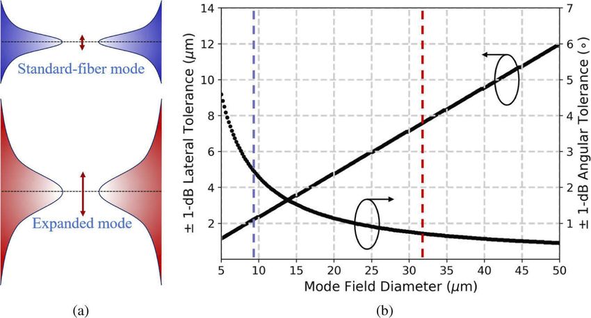
Research Article                                  Vol. 29, No. 5 / 1 March 2021 / Optics Express   7603

a photonics chip interposer [39]. A backside coupling interface in this scenario allows a high
density optical I/O for high speed transfer of data across the server backplanes [40,41].
   An initial demonstration of a monolithic backside coupling interface was showcased recently
[38], but it was targeted towards the wavelength range of C-band and a system-level analysis
was not performed at that time. Also, the discussion in our earlier work was only limited
to the alignment tolerant aspect of the concept, but did not provide the coupling analysis in
greater detail. Moreover, the fiber-to-fiber coupling results presented in our previous work
were obtained by using a multimode fiber as the output fiber. In comparison, in this paper, we
provide a complete single-mode fiber-to-fiber coupling analysis for a target wavelength range
in O-band, and investigate the individual contributions in coupling loss of an expanded beam
interface. Based on these results, we provide suggestions for future improvements and project
the net reduction in overall loss that can be achieved in a monolithically fabricated expanded
beam interface. Also, in comparison to our previous work on Si microlenses using hybrid
integration [37], this paper discusses the generic design challenges in greater detail incorporating
all the parametric degrees of freedom in the design space, when implementing expanded beam
coupling interfaces for integrated photonics chips for any wavelength range and material platform.
Separately, both top-side and back-side coupling and testing strategies are explored to arrive
at an optimum coupling performance of the expanded beam interface. This also generates
different application-dependent integration possibilities for a designer targeting to implement the
concept. Lastly, by integrating microlenses monolithically, the paper demonstrates the potential
of extending this concept at wafer-scale for alignment-tolerant optics across different material
platforms.

2.   Generic concept and design principles to realize An expanded beam cou-
     pling interface
The concept of expanded beam collimation in itself is very generic, and can be implemented for
other wavelength bands and material platforms for integrated optics (e.g. SiN, InP etc.), as long as
the substrate material is transparent to a corresponding wavelength range. The operating principle
of expanded beam collimation using a photonics chip integrated with backside microlenses is
as follows: the photonics chip consists of downward directionality based grating couplers that
diffract the incoming optical waveguide mode at an angle into the bulk silicon substrate. The
diffracted beam expands in the silicon substrate and is collimated with the help of a microlens
with a particular radius of curvature. The expanded and collimated optical beam from the
backside microlens is then coupled into a thermally expanded-core (TEC) fiber with a similar
mode-field diameter (Fig. 2). The enlarged mode field diameter of a thermally expanded core

              Fig. 2. An overview of photonics chip expanded-beam coupling interface.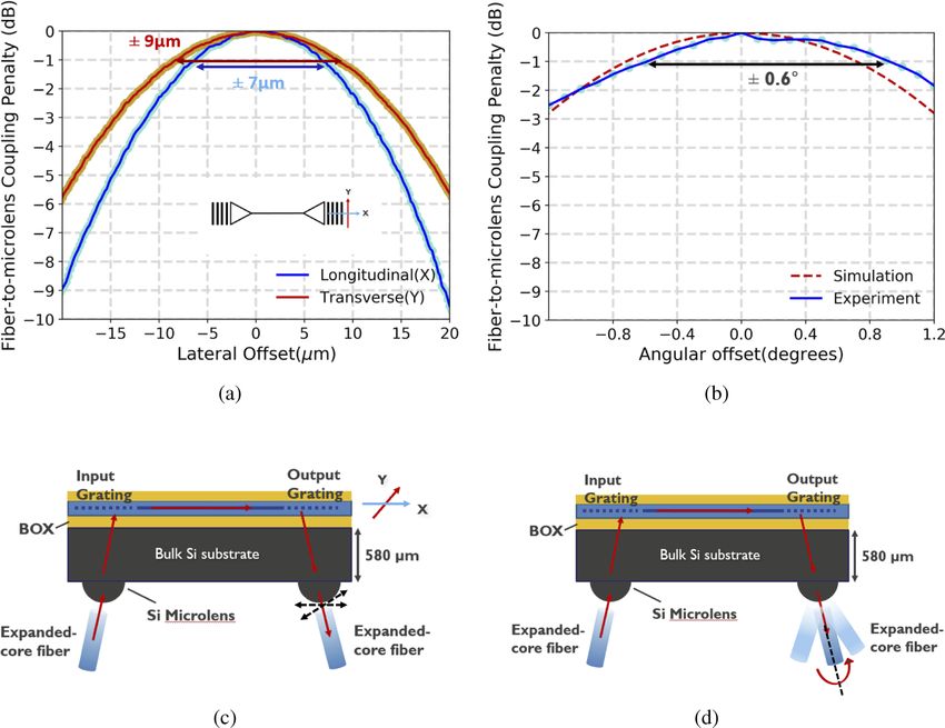
Research Article                                      Vol. 29, No. 5 / 1 March 2021 / Optics Express   7604

(TEC) fiber is obtained by locally heating a single-mode fiber at high temperature resulting in the
redistribution of dopants while maintaining the single-mode condition of the fiber [42,43]. As an
alternative, a fiber-lens assembly optimized for a collimated beam of a particular diameter can
also be used to perform coupling. The results presented here, however have been achieved with
the commercially available TEC fibers. To realize such an expanded beam interface, there are
some design parameters and boundary conditions (Fig. 3) that need to be evaluated based on the
desired final metrics such as final beam diameter, 1-dB lateral and angular alignment tolerance,
wavelength range of operation, coupling efficiency etc.

       Fig. 3. (a) A schematic of the expanded beam coupling concept using backside emitting
       grating couplers, highlighting the parameters available for design and (b) tabulated with the
       description of those parameters.

   (i) Starting mode-field diameter, Wstart : The mode-field diameter of the optical beam diffracted
by the output grating coupler is a critical parameter to determine the final expanded beam
diameter, which also depends on the propagation distance (as described in (ii)) and refractive
index of the silicon substrate. Besides the mode-field diameter, the field profile emitted from the
grating dictates the overall transformation of the beam as it propagates down the substrate and
impacts the coupling performance eventually. Thus, an appropriate grating design is required to
accomplish the desired metrics.
   (ii) Thickness of the substrate, Tsub : The propagation distance of the diffracted beam between
the grating and the microlens is determined by Tsub /cos(θ Si ), where θ Si is the angle of the
diffracted beam with respect to normal in the silicon substrate. Thus, various values of expanded
beam diameters can be obtained by a conscious choice of substrate thickness and a starting beam
diameter at the grating coupler. Assuming Gaussian beam propagation with an initial waist of
4.6 µm (diameter - 9.2 µm) from the designed grating coupler, at an O-band primary wavelength
of λ = 1310 nm, the resulting beam diameters (at the microlens) as a function of silicon substrate
thickness have been listed in Table 1.
   (iii) Angle of the beam in Silicon, θ Si : This parameter is related to the period of the designed
grating and determines the resultant propagation distance of the beam in the chip substrate. It also
determines the offset that has to be provided to shift the center of the microlens with respect to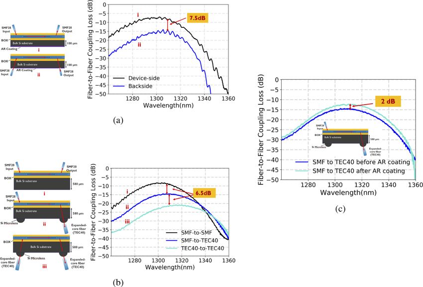
Research Article                                   Vol. 29, No. 5 / 1 March 2021 / Optics Express   7605

         Table 1. A list of the values of the expanded beam diameter and required radius of
          curvature (ROC) of the microlens to achieve beam collimation corresponding to
          different thicknesses of the silicon chip substrate. Starting beam waist = 4.6 µm
                             (diameter = 9.2 µm), θSi = 4.06◦ , λ = 1310 nm.
       Si Substrate Thickness (µm)   Expanded Beam Diameter (µm)       Radius of Curvature (µm)
                   200                           13.4                               205
                   300                           16.9                               245
                   400                           21.7                               310
                   500                           26.2                               370
                   600                           31.0                               440
                   700                           36.3                               515

the coupling position of the grating and hence, ensure that the beam is incident in an appropriate
region of the microlens. As an example, for a grating coupler diffracting at 10◦ angle in oxide,
the corresponding beam angle in silicon is 4.06◦ .
   (iv) Lens offset from the optimum coupling position of the grating, OL : Since the beam
diffracted from the grating is directed at a certain angle θ Si into the substrate, the center of the
microlens has to be shifted by an offset OL to ensure that the expanded optical beam hits an
appropriate region of the microlens and gets collimated in the direction of the fiber. An improper
placement of the microlens with respect to the grating might lead to a shift in the exit angle of
the beam from the microlens, which would impact the coupling efficiency and/or a shift in the
coupling spectrum (with the assumption that the position of the single-mode fiber or optical
readout is fixed). As shown earlier in Fig. 1, the angular tolerance of the expanded beam reduces
as the beam diameter increases. Thus, the larger the target beam diameter for an application, the
more critical the lens offset parameter will be.
   (v) Radius of curvature of the microlens, RL : While the parameters (i)-(iii) determine the
extent of the expansion of the beam, the collimation of the beam is achieved by calculating
a specific radius of curvature of the microlens. A positive deviation of this value results in a
divergent beam which is not fruitful to obtain a large longitudinal and lateral alignment tolerance
from the interface. On the other hand, a negative deviation of this value results in a convergent
beam that can perhaps be used to design an interface with a large working distance between the
fiber and the microlens (with a limitation of requiring longer propagation distance between the
grating and the microlens, and therefore, a thicker substrate). Considering the same conditions as
mentioned in (ii), the corresponding values of RL for different substrate thickness have been listed
in Table 1. These values have been obtained from the Gaussian beam propagation method using
a model designed in OpticStudio (Zemax) [37,44]. Since the microlens is spherical here, the
beam angle, applied offset, and the calculated ROC are valid under the assumption of principal
rays being orthogonal to the surface of the microlens.
   (vi) Fiber mode-field diameter, Wfiber : The expanded collimated beam from the microlens
placed at the chip backside is coupled to either an expanded beam interface such as a fiber array
with integrated microlenses or a fiber with an expanded mode-field diameter as depicted in Fig. 2.
Thus, the mode-field diameter of the out-coupling interface, Wfiber , is one of the target metrics
that governs the parameters (i)-(iii).
   All of these parameters hold key value in reaching the target of increased coupling tolerance to
lateral and longitudinal misalignment. In the following sections in this paper, the system-level
design is discussed for a specific case in O-band, but it should be noted that the generic design
principles described in this section can also be applied for a different wavelength band (e.g.
C-band), provided the grating design, beam diameter, beam divergence, chip substrate thickness,
chip backside AR coating and microlens parameters are adjusted accordingly.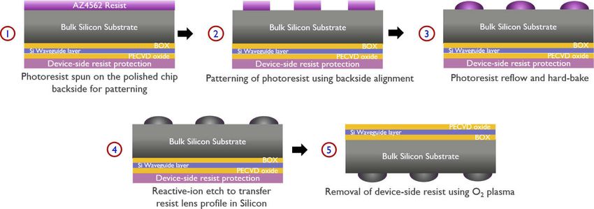
Research Article                                    Vol. 29, No. 5 / 1 March 2021 / Optics Express   7606

3.   System-level optical design
The generic design principles described in the previous section were applied to a specific case of a
photonics chip consisting of grating couplers operating around 1310 nm wavelength and a desired
collimated beam diameter of 32 µm (beam diameter being dictated by the commercially available
TEC fibers used for characterization). With these boundary conditions fixed, the thickness of the
chip substrate was determined to be 600 µm, which resulted in a target ROC of 440 µm for the
microlens. Also, the microlens was placed at an offset of 43 µm with respect to the coupling
position of the uniformly periodic grating coupler (Fig. 3). This offset was computed by taking
into account a 4.06◦ grating diffraction angle in silicon (600 µm × tan4.06◦ ). Although grating
couplers with metal reflectors deposited on top oxide provide high directionality towards the
direction of the substrate [45,46], the experiment was performed on photonics dies consisting of
regular grating couplers (Λ = 490 nm, fill-factor = 0.5) without the metal reflectors to facilitate
fiber-coupling tests from both sides of the chip, and hence, provide ease in evaluation of various
contributing factors of losses incurred in the expanded beam interface, as detailed in Section 5
   The design schematic shown in Fig. 3(a) was directly implemented in Zemax OpticStudio and
has been described in our previous work [37]. From the Zemax model, a sensitivity analysis of
the coupling efficiency was carried out by varying the radius of curvature (ROC) of the microlens.
Figure 4 shows the effect of variability of the ROC of the microlens on the resultant beam diameter
and relative coupling efficiency to an expanded core fiber placed 100 µm distance away from the
vertex of the microlens. The variation in beam diameter would occur due to the converging or
diverging nature of the beam for a non-ideal value of ROC of the microlens, and results in a drop
in the coupling efficiency. It was found that for a 1-dB tolerance in coupling efficiency to an
expanded core fiber, a −100 µm and +180 µm variation in the ROC of the microlens is allowed.
Although such numbers indicate a large tolerance of the ROC on fiber coupling efficiency at a
given distance from the microlens, it should be noted that the beam collimation is affected as the
ROC of the microlens deviates from an ideal value, which reduces the longitudinal alignment
tolerance.

       Fig. 4. For a 1-dB tolerance in coupling efficiency to an expanded core fiber, a −100 µm
       and +180 µm variation in the radius of curvature of the microlens was obtained.

4.   Fabrication process flow
The fabrication of microlenses in silicon using resist reflow and reactive ion etching (RIE) has
been widely investigated over several years and is a fairly mature technology now [47,48]. For the
fabrication of silicon microlenses directly at the backside of the photonics chip, it was necessary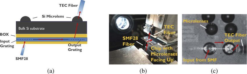
Research Article                                      Vol. 29, No. 5 / 1 March 2021 / Optics Express   7607

       Fig. 5. Process flow for the fabrication of Si microlenses at the photonics chip backside.

that not only the microlenses were aligned and etched optimally with respect to the grating
structures on the chip frontside, but also the SOI chip was backside polished and protected well
from the front-side during processing. The process flow that was followed is illustrated in Fig. 5.
Firstly, the photonics chip substrate was thinned and polished from the backside to a thickness of
600 µm [49]. The chip thickness was well-controlled in the central region where the lenses were
fabricated in a later stage, the variation being ±1 µm when introducing intermediate thickness
measurements during thinning. The rms surface roughness obtained after polishing the chip
is between 10-15 nm measured on an area of 1×1 cm2 . This is lower than (λ/nSi )/20 and can
therefore be considered as an optically smooth surface. To begin processing on the backside
of the photonics die for the fabrication of microlenses, the frontside of the die was protected
by a photoresist layer. With the frontside of the die protected, the polished backside was spin
coated with Microchem AZ4562 resist. To fabricate the lenses with a desired ROC (440 µm) in
silicon, it is important that the resist thickness after spinning is well-controlled [50]. The target
thickness of the resist here was 11.5 µm. The lithographic patterning of the microlens structures
was performed using a dual-sided EVG mask aligner. This step is very critical, to ensure a
backside-to-frontside alignment accuracy below ±1 µm. After the patterns were exposed, and
the exposed resist was removed during a developing step, the obtained cylindrical structures were
reflowed at 145◦ C and hard-baked in an oven at 120◦ C. Thereafter, photoresist microlenses were
transferred into silicon by an optimized reactive ion etch (RIE) process employing a mixture of
SF6 and O2 . The resist protection on the frontside of the photonics chip was removed later with
the help of an O2 plasma.
   After fabrication, the microlenses were characterized using a white-light optical profilometer,
and an ROC of 420 µm was obtained that was less than the target value by only 4.5% (Fig. 6).
Also, an rms roughness of less than 10 nm was measured over the central region of the microlens
spanning an area of 40×40 µm2 . Furthermore, the backside alignment accuracy after step 2,
was estimated by inspecting the sample under a near IR-enabled diascopic illumination mode
of the microscope. This enabled a through-substrate view of the photonics chip, viewed from
the backside of the die. The microlenses were fitted with a circle and reference structures at the
front side of the die were measured with respect to the fitted circle, as shown in Fig. 7(b). On
comparing the measurements with those from the GDS design file (Fig. 7(a)), a difference in
alignment of within ±1 µm was obtained along both the directions of the grating. This indicates
an actual alignment accuracy close to ±1 µm, although the accuracy of the applied measurement
method is not exactly known. To avoid any ambiguity, it must be noted that Fig. 6(a) depicts
the testsite of grating-to-grating link with microlenses in resist and is shown here for illustration
purposes.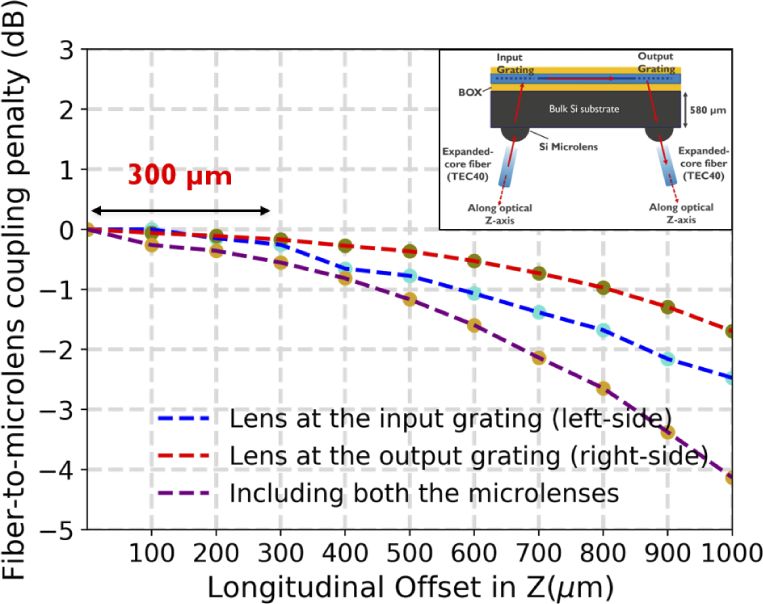
Research Article                                    Vol. 29, No. 5 / 1 March 2021 / Optics Express   7608

       Fig. 6. (a) Diascopic near-IR view of the microlenses formed in resist; (b) Microscope
       image of the etched microlens; (c) A surface profilometer scan of microlens post-etch to
       determine the resulting diameter, sag and radius of curvature of the silicon microlens.

       Fig. 7. (a) GDS design location of the grating structures with respect to the designed
       microlenses and (b) Diascopic (transmitted) NIR illuminated image from the microscope of
       the same design location. On comparing the markers with those from the GDS design file, a
       difference in microlens alignment of within ±1 µm was obtained along both the directions
       of the grating coupler.

5.   Experiment and results
Since the chip consisted of regular uniformly periodic grating couplers and metal reflectors
were not deposited above the grating, both the topside and the backside fiber coupling options
were available. While a standard single-mode fiber (SMF28, MFD - 9.2 µm, NA - 0.14) was
used to perform coupling from the topside of the chip, a thermally expanded core single-mode
fiber (MFD - 32±2 µm, NA - 0.02) was used to couple the beam from the chip backside using
microlens. Firstly, SMF28 fibers were used to couple in and out of the input and the output
gratings from the device-side (topside) of the chip. Then, keeping the input fiber alignment
with the grating intact, the optical beam exiting the microlens is coupled (from the backside of
the chip) into a thermally expanded core fiber (TEC40) (Fig. 8). In this configuration, both the
lateral and the angular alignment of the TEC40 fiber could be performed against the microlens
fabricated with respect to the output grating, and a single microlens-to-fiber collimation property
could be assessed. After the optimization of the backside fiber alignment with respect to the
output microlens, the fiber input was shifted from the frontside to the backside of the die. The
input fiber was also changed from SMF28 to TEC40 and aligned actively with respect to the
microlens fabricated with respect to the input grating. Thus, an expanded mode coupling could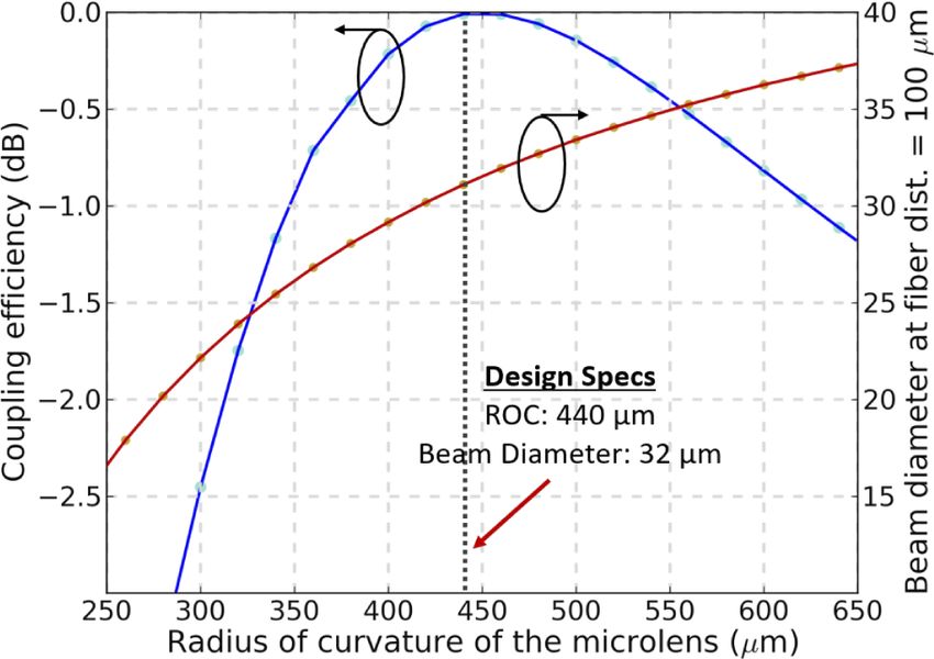
Research Article                                        Vol. 29, No. 5 / 1 March 2021 / Optics Express   7609

      Fig. 8. Measurement methodology to align one TEC fiber with the microlens: The input
      fiber (SMF28) was used to launch the optical beam into the grating from the front-side of the
      die. The uniformly periodic output grating diffracts a part of the guided waveguide mode
      into the substrate that is coupled to the thermally expanded core fiber (TEC40) from the chip
      backside using the fabricated microlenses.

be performed from both the ends of the grating to evaluate the combined performance of the
input and the output fiber-microlens system.

      Fig. 9. (a) A comparison of (i) frontside vs. (ii) backside fiber-to-fiber coupling loss has been
      made for regular O-band grating couplers with a 490 nm period and 0.5 fill-factor; (b) The
      efficiency of the expanded beam interface was evaluated by comparing three measurements:
      (i) frontside SMF-to-SMF coupling loss, (ii) SMF (frontside)-to-TEC40 (backside) coupling
      loss and (iii) TEC40 (backside)-to-TEC40 (backside) coupling loss. Comparing graphs
      9a.(ii) and 9b.(iii) results in an additional penalty of 3 dB due to increase in substrate
      thickness, the microlens, and the absence of AR coating; (c) An improvement of 2 dB
      in coupling efficiency was measured after the deposition of anti-reflection coating on the
      backside microlenses.

  Since regular grating couplers were used to perform this experiment, firstly, a frontside versus
backside coupling efficiency was measured using standard single-mode fibers (SMF28) on a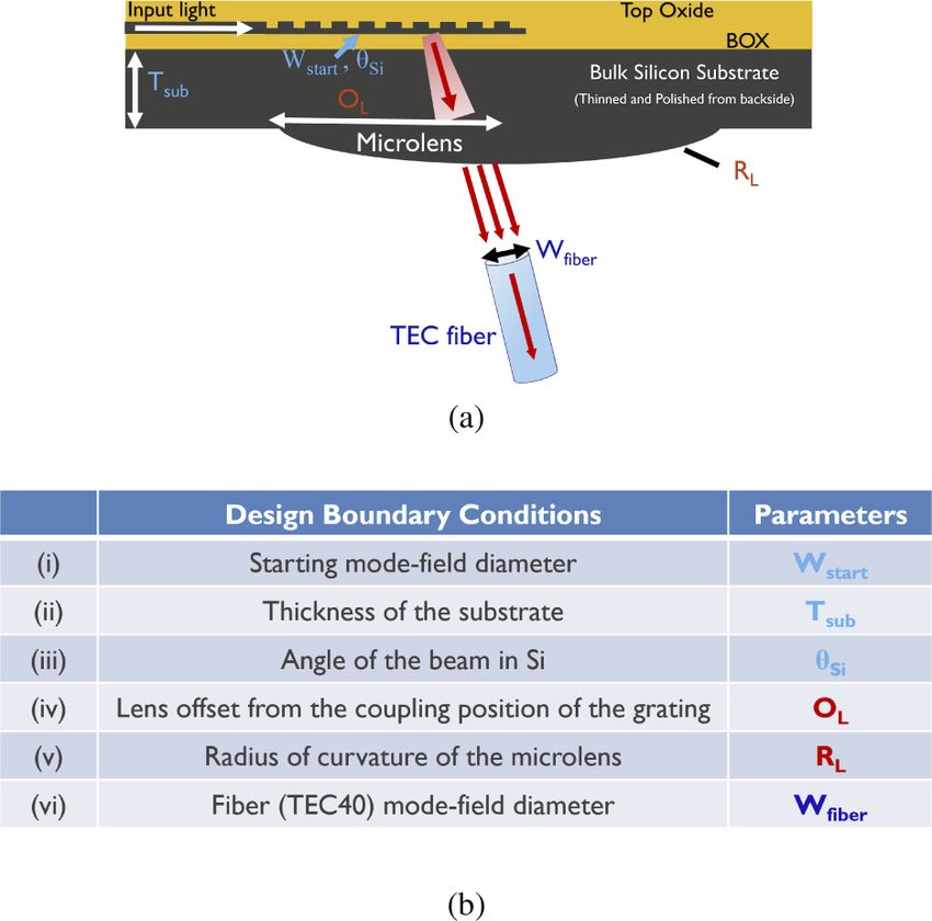
Research Article                                          Vol. 29, No. 5 / 1 March 2021 / Optics Express   7610

different chip with a substrate thickness of 100 µm, polished and AR-coated from the backside.
This measurement provided a good reference to compare against the subsequent backside coupling
measurements and thereby, deduce the coupling loss from a single expanded beam interface.
Also, it is to be noted that the microlens and the grating coupler on either side of input/output
is a combined entity, due to which the effect of each on the coupling efficiency cannot be
separated out based on the current measurements. However, based on comparisons between
different fiber-to-fiber coupling configurations and chip substrate thicknesses, the contribution
of the combined grating-microlens entity to the loss can be derived and a projection can be
made for further reduction of the loss when employing improved grating designs. As shown in
Fig. 9(a) (depicting fiber-to-fiber coupling loss), an additional 3.75 dB loss per fiber-to-grating
coupler interface occurs on shifting the fiber from the frontside (graph 9(a.i)) to the backside
(graph 9(a.ii)) of the chip (with a lower net downward directionality due to Fresnel reflections from
the BOX-silicon interface). Next, for the chip with the microlenses fabricated at its backside, the
measured spectrum for SMF28 (frontside)-to-TEC40 (backside) and TEC40 (backside)-to-TEC40
(backside) configurations are shown via graphs 9(b.ii) and 9(b.iii) respectively in Fig. 9(b). The
red shift of the center wavelength in graphs 9(b.ii) and 9(b.iii) is likely an outcome of using a
thick substrate for beam expansion and the slope of absorption coefficient in bulk Si in O-band
[51]. On comparing the graph 9(a.ii) and graph 9(b.iii), a difference of 6 dB in fiber-to-fiber
backside coupling loss is obtained i.e. a 3 dB coupling loss is introduced in a single expanded
beam interface due to the increase in substrate thickness, the microlens itself and the absence of
AR coating on the microlens.

                  Table 2. Optical Loss Contribution In An Expanded Beam Interface
                               Measured Parameters                                           Loss
         Backside coupling loss of a uniform grating (100 µm chip substrate                7.5 dB
                              thickness) - Fig. 9(a.ii)
         Improvement margin in coupling loss of expanded beam interface after                2 dB
                     the application of AR coating - Fig. 9(c)
         Coupling loss in a single grating-microlens expanded-beam interface               8.5 dB
             (580 µm chip substrate thickness) - Fig. 9(b.iii) & Fig. 9(c)
         Projected coupling loss in a grating-microlens single expanded-beam       uniform          < 2.8 dB
                interface employing gratings with metal reflectors and
                 grating-to-microlens placement accuracy < ±0.5 µm                apodized          < 2 dB

   Out of this additional 3 dB coupling loss, a 1.85 dB loss contribution was expected due to
the Fresnel reflections from the silicon-air interface. This can be corrected by depositing an
antireflective coating on the microlenses. To address this point, measurements were performed
again on a single expanded beam interface after the deposition of 170 nm thick SiN anti-reflective
(AR) coating. As can be seen via Fig. 9(c), an improvement of 2 dB was measured in the fiber
(SMF)-to-fiber (TEC40) coupling efficiency. Also, no impact on the resultant bandwidth of the
optical output was observed. A slightly higher improvement in coupling efficiency than the
expected value indicates higher reflection of the beam that hits off-normal to the surface of the
microlens, when the AR coating is not present. The cause of the remaining 1 dB loss from a
single expanded beam interface can probably be attributed to the mode-profile mismatch due
to the exponentially decaying field profile from the grating. Also, from the backside alignment
analysis of microlens with respect to the grating that was reported earlier [37], a 0.5 dB coupling
penalty can occur even if the fabricated microlenses are misplaced by ±1-1.5 µm from the desired
location with respect to the grating. The applied offset of the microlens with respect to the grating
coupler could also be improved after conducting a detailed design of experiment (DOE) during
wafer-scale fabrication that can also account for the variability in beam angle from the grating at
the intended wavelength of operation and radius of curvature of the microlens (Fig. 4). Thus, the
Research Article Vol. 29, No. 5 / 1 March 2021 / Optics Express 7611
expanded beam coupling interface contributes to an additional 0.5-1 dB loss to the fiber-to-fiber
link budget, implying that majority of the losses are incurred from the grating coupler itself.
It should be noted, as mentioned before, this paper is focused on realizing a monolithic
expanded beam interface, and not to obtain the lowest possible total fiber-to-fiber loss. By
decoupling the different losses, it is evident that minimizing the losses from the grating coupler
will reduce the overall coupling penalty. This can be achieved by depositing metal reflectors above
the grating couplers to improve the directionality and thereby, the overall fiber-to-fiber coupling
performance, as has been reported via a hybrid integration experiment earlier (regular grating
backside coupling efficiency used here being −7.5 dB in comparison to coupling efficiency
of a backside grating with metal reflector being −2.3 dB) [37,45]. Thus, by improving the
grating-to-microlens alignment accuracy to ±0.5 µm [37], and employing uniform gratings with
metal reflectors, a single expanded beam interface incurring a 8.5 dB loss in this demonstration
can be optimized further to lower the loss to 2.8 dB (8.5 - (7.5-2.3)- 0.5 = 2.8) or less. Moreover,
if apodized gratings with metal reflectors are used (fiber-to-grating coupling efficiency ∼ −1.5
dB [46]), the coupling loss of the expanded beam interface can be lowered down further to < 2
dB (8.5 - (7.5-1.5)−0.5 = 2), as projected in Table 2.
To assess the fiber-to-microlens alignment tolerance, an active alignment scan of the expanded
core fiber was performed with respect to the microlenses at the backside of the chip. A ±7 µm and
a ±9 µm 1-dB lateral alignment tolerance of the expanded core fiber was measured with respect
to the longitudinal (X) and transverse (Y) axes of the grating coupler (Fig. 10(a)). This slight
difference was expected because of the asymmetric size of the beam diffracted by the grating
Fig. 10. (a,c) A ±7 µm and ±9 µm 1-dB alignment tolerance with respect to the longitudinal
(X) and transverse (Y) axes of the grating and (b,d) ±0.6◦ angular 1-dB alignment tolerance
was measured between an expanded mode coupled from the microlens to a single-mode
expanded-core fiber.Research Article Vol. 29, No. 5 / 1 March 2021 / Optics Express 7612
coupler in both of the orthogonal directions [52]. Also, a ±0.6◦ angular 1-dB alignment tolerance
was measured between the microlens and the expanded core fiber (Fig. 10(b)). These values are
similar to those reported earlier by us in the hybrid integration experiment using microlenses at
the backside of the photonics chip with a similar thickness of the silicon substrate [36].
Lastly, on retracting the expanded core fiber away from the microlens vertex successively in
steps of 100 µm along the axis of the output beam, the fiber-to-microlens coupling efficiency was
recorded at a fixed wavelength of 1310 nm. Fig. 11 shows that a 0.2 dB drop in the coupling
efficiency was measured over a distance of 300 µm, when either of the input or the output fiber
was retracted away from the microlens. Also, when both of the fibers were retracted together, a
1-dB coupling penalty occurs for a microlens-to-fiber separation of 400 µm. This is an outcome
of the collimated nature of the beam, and also indicative of a large tolerance available in the
longitudinal direction for an expanded beam connection.
Fig. 11. On retracting the fibers individually along the axis of propagation of the collimated
beam, a 0.2 dB drop in the coupling efficiency was measured over a distance of 300 µm.
When both the fibers were retracted together, a 400 µm 1-dB longitudinal alignment tolerance
was measured.
6. Discussion
It should be noted that the commercial availability and wide choice of mode field diameters of
TEC fibers helped us to demonstrate the concept using these fibers. Clearly, these fibers can be
replaced by a single-mode fiber ribbon mounted with a microlens array block, and can be used in
the future to implement the presented concept. As can be noticed from the demonstrated results,
the size of the microlens seems to be a limiting factor for applications addressing high on-chip
and off-chip wiring density. In such a scenario, if fiber-ribbon arrays of 127 or 250 µm fiber pitch
are used, lenses with low clear aperture would need to be fabricated to accommodate the high
on-chip wiring density. It is to be noted that a lens of 270 µm diameter has been fabricated in our
demonstration, and this value can be shrunk further by modifying the lens height to lens diameter
ratio without changing the radius of curvature, if needed [53]. Moreover, if further increase in
wiring density (and hence, lens diameter and pitch reduction) is required, other methods such
as grayscale lithography, imprinting, direct writing based on 2-photon polymerization could be
used. The design trade-off in that case would be to limit the beam expansion and hence, obtain a
limited gain in the lateral alignment tolerance.
Although fibers have been used to demonstrate the concept of expanded beam coupling, the
coupling to the microlens can be provided directly via a laser or VCSEL for specific applications.
In that case a suitable microlens can be used to ensure that the laser/VCSEL emits a collimated
beam with the desired diameter. A potential challenge will be to additionally provide the electricalResearch Article Vol. 29, No. 5 / 1 March 2021 / Optics Express 7613 connections and to keep the form-factor of the entire module compact, and tackle the associated integration and assembly-level issues. This will depend on the type of laser. For a VCSEL, which is surface emitting, this seems very feasible, since a microlens can directly be mounted on top of the emitter, while for an edge-emitting laser, a mirror would have to be integrated to rotate the beam by 90 degrees to couple it to the microlens. The key advantage of integrating the microlenses at the backside of the photonics chip is an increased tolerance to the lateral misalignment. Clearly, this is obtained at the expense of a reduced tolerance to angular misalignment in the coupling interface. The angular tilts, however, can be compensated or controlled more easily during assembly compared to lateral misalignments. Studies have already indicated a chip angular alignment accuracy of ±0.1◦ , with a potential to achieve further improvement in passive assembly [29]. Thus, the demonstration of monolithically fabricated coupling interface is an attractive proposition to perform alignment-tolerant coupling in sensing applications or chip-to-board coupling for the face-up integration of a silicon photonics interposer. 7. Conclusion We have reported results for monolithic integration of microlenses directly at the backside of a silicon photonics chip with a goal to achieve alignment-tolerant expanded beam interface. The design choices, fabrication process flow, and fiber coupling and alignment methodology were described comprehensively. A detailed investigation of the coupling performance and fiber-to-microlens alignment tolerance was carried out to underline the advantages of a SOI integrated photonics chip based expanded beam coupler. In particular, the expanded beam coupling interface adds a very small additional loss (0.5-1 dB) to the overall budget, with majority of the losses incurred from the grating coupler itself. By employing gratings with metal reflectors and < ±0.5 µm microlens-to-grating placement accuracy, losses under 2 dB have been projected for a monolithically integrated grating-microlens expanded beam interface. With an expanded beam diameter of 32 µm, a ±7 µm lateral and a ±0.6◦ angular fiber-to-microlens 1-dB alignment tolerance was obtained at the wavelength of 1310 nm. Also, a large 300 µm longitudinal alignment tolerance with a 0.2 dB drop in coupling efficiency was obtained when the coupling was performed into a thermally expanded core (TEC) single-mode fiber. These relaxed alignment tolerance values are possible to obtain with wafer-scale backside integrated microlenses and can pave the way to perform coupling to a fiber array with a longer working distance or provide high-density on-board optical solution in the near future. Acknowledgments. The primary author would like to thank the entire SiPh integration team at imec for providing help with the silicon photonics dies fabricated from 200-mm wafer-scale processing. Acknowledgments are also extended to Filip Vermeiren and Stijn Duynslager, CMST, Ghent University for their help with reactive-ion etching of microlenses and die-lapping respectively and Photonics Research Group (INTEC Department), Ghent University for help with SiN deposition. This work has been carried out as part of imec’s industry affiliation program on Optical I/O, and the AQUARIUS project. The AQUARIUS project has received funding from the European Union’s Horizon 2020 research and innovation programme under grant agreement No. 731465. This project is an initiative of the Photonics Public Private Partnership. Disclosures. The authors declare that there are no conflicts of interest related to this article. References 1. X. Chen, M. M. Milosevic, S. Stanković, S. Reynolds, T. D. Bucio, K. Li, D. J. Thomson, F. Gardes, and G. T. Reed, “The emergence of silicon photonics as a flexible technology platform,” Proc. IEEE 106(12), 2101–2116 (2018). 2. A. Rahim, T. Spuesens, R. Baets, and W. Bogaerts, “Open-access silicon photonics: current status and emerging initiatives,” Proc. IEEE 106(12), 2313–2330 (2018). 3. M. Binda, A. Canciamilla, A. Daverio, A. Fincato, P. Gambini, L. Maggi, P. Orlandi, L. Ramini, M. Repossi, A. Simbula, and M. Shaw, “High capacity silicon photonics packaging,” in 2019 22nd European Microelectronics and Packaging Conference & Exhibition (EMPC), (IEEE, 2019), pp. 1–8. 4. A. Mekis, T. Pinguet, G. Masini, S. Sahni, M. Mack, S. Gloeckner, and P. De Dobbelaere, “Advanced silicon photonics transceivers,” in Silicon Photonics III, (Springer, 2016), pp. 349–374.
Research Article                                               Vol. 29, No. 5 / 1 March 2021 / Optics Express   7614

5. H. Yu, J. Doylend, W. Lin, K. Nguyen, W. Liu, D. Gold, A. Dahal, C. Jan, R. Herrick, G. A. Ghiurcan, S. R.
    Hollingsworth, R. T. Romero, M. E. Favaro, L. Qiu, D. Zhu, and Y. Akulova, “100gbps cwdm4 silicon photonics
    transmitter for 5g applications,”, in Optical Fiber Communication Conference, (Optical Society of America, 2019),
    pp. W3E–4.
6. M. J. Heck, “Highly integrated optical phased arrays: photonic integrated circuits for optical beam shaping and beam
    steering,” Nanophotonics 6(1), 93–107 (2017).
7. C. V. Poulton, A. Yaacobi, D. B. Cole, M. J. Byrd, M. Raval, D. Vermeulen, and M. R. Watts, “Coherent solid-state
    lidar with silicon photonic optical phased arrays,” Opt. Lett. 42(20), 4091–4094 (2017).
8. I. Staude and J. Schilling, “Metamaterial-inspired silicon nanophotonics,” Nat. Photonics 11(5), 274–284 (2017).
9. M. Khorasaninejad and F. Capasso, “Metalenses: Versatile multifunctional photonic components,” Science 358(6367),
    eaam8100 (2017).
10. S. A. Miller, M. Yu, X. Ji, A. G. Griffith, J. Cardenas, A. L. Gaeta, and M. Lipson, “Low-loss silicon platform for
    broadband mid-infrared photonics,” Optica 4(7), 707–712 (2017).
11. J.-M. Fedeli and S. Nicoletti, “Mid-infrared (mid-ir) silicon-based photonics,” Proc. IEEE 106(12), 2302–2312
    (2018).
12. L. R. Chen, “Silicon photonics for microwave photonics applications,” J. Lightwave Technol. 35(4), 824–835 (2017).
13. J. S. Fandiño, P. Muñoz, D. Doménech, and J. Capmany, “A monolithic integrated photonic microwave filter,” Nat.
    Photonics 11(2), 124–129 (2017).
14. D. J. Moss, R. Morandotti, A. L. Gaeta, and M. Lipson, “New cmos-compatible platforms based on silicon nitride
    and hydex for nonlinear optics,” Nat. Photonics 7(8), 597–607 (2013).
15. M. Borghi, C. Castellan, S. Signorini, A. Trenti, and L. Pavesi, “Nonlinear silicon photonics,” J. Opt. 19(9), 093002
    (2017).
16. J. W. Silverstone, J. Wang, D. Bonneau, P. Sibson, R. Santagati, C. Erven, J. O’Brien, and M. Thompson, “Silicon
    quantum photonics,”, in 2016 International Conference on Optical MEMS and Nanophotonics (OMN), (IEEE, 2016),
    pp. 1–2.
17. T. Rudolph, “Why i am optimistic about the silicon-photonic route to quantum computing,” APL Photonics 2(3),
    030901 (2017).
18. Y. Shen, N. C. Harris, S. Skirlo, M. Prabhu, T. Baehr-Jones, M. Hochberg, X. Sun, S. Zhao, H. Larochelle, D.
    Englund, and M. Soljačić, “Deep learning with coherent nanophotonic circuits,” Nat. Photonics 11(7), 441–446
    (2017).
19. D. A. Miller, “Silicon photonics: Meshing optics with applications,” Nat. Photonics 11(7), 403–404 (2017).
20. Q. Cheng, J. Kwon, M. Glick, M. Bahadori, L. P. Carloni, and K. Bergman, “Silicon photonics codesign for deep
    learning,” Proc. IEEE (2020).
21. A. N. Tait, T. F. De Lima, E. Zhou, A. X. Wu, M. A. Nahmias, B. J. Shastri, and P. R. Prucnal, “Neuromorphic
    photonic networks using silicon photonic weight banks,” Sci. Rep. 7(1), 7430 (2017).
22. A. Katumba, M. Freiberger, F. Laporte, A. Lugnan, S. Sackesyn, C. Ma, J. Dambre, and P. Bienstman, “Neuromorphic
    computing based on silicon photonics and reservoir computing,” IEEE J. Sel. Top. Quantum Electron. 24(6), 1–10
    (2018).
23. R. Marchetti, C. Lacava, L. Carroll, K. Gradkowski, and P. Minzioni, “Coupling strategies for silicon photonics
    integrated chips,” Photonics Res. 7(2), 201–239 (2019).
24. B. W. Snyder, “Hybrid integration and packaging of grating-coupled silicon photonics,” Ph.D. thesis, University
    College Cork (2013).
25. T. Barwicz, Y. Taira, T. W. Lichoulas, N. Boyer, Y. Martin, H. Numata, J.-W. Nah, S. Takenobu, A. Janta-Polczynski,
    E. L. Kimbrell, R. Leidy, M. W. Khater, S. Kamlapurkar, S. Engelmann, Y. A. Vlasov, and P. Fortier, “A novel
    approach to photonic packaging leveraging existing high-throughput microelectronic facilities,” IEEE J. Sel. Top.
    Quantum Electron. 22(6), 455–466 (2016).
26. G. B. Preve, “Problems, challenges, and a critical survey on automated silicon photonics packaging and optical
    interconnection,” in Optical Interconnects XIX, vol. 10924 (International Society for Optics and Photonics, 2019), p.
    1092415.
27. T. Barwicz, T. W. Lichoulas, Y. Taira, Y. Martin, S. Takenobu, A. Janta-Polczynski, H. Numata, E. L. Kimbrell, J.-W.
    Nah, B. Peng, D. Childers, R. Leidy, M. Khater, S. Kamlapurkar, E. Cyr, S. Engelmann, P. Fortier, and N. Boyer,
    “Breaking the mold of photonic packaging,” in Integrated Optics: Devices, Materials, and Technologies XXII, vol.
    10535 (International Society for Optics and Photonics, 2018), p. 105350R.
28. W. Joyce and B. DeLoach, “Alignment of gaussian beams,” Appl. Opt. 23(23), 4187–4196 (1984).
29. S. D. Le, P. Rochard, J.-B. Briand, L. Quétel, S. Claudot, and M. Thual, “Coupling efficiency and reflectance analysis
    of graded index expanded beam connectors,” J. Lightwave Technol. 34(9), 2092–2099 (2016).
30. T. Barwicz, N. Boyer, A. Janta-Polczynski, J.-F. Morissette, Y. Thibodeau, L. Patry, T. W. Lichoulas, E. L. Kimbrell, S.
    Martel, S. Kamlapurkar, S. Engelmann, R. L. Bruce, Y. A. Vlasov, and P. Fortier, “A metamaterial converter centered
    at 1490nm for interfacing standard fibers to nanophotonic waveguides,” in 2016 Optical Fiber Communications
    Conference and Exhibition (OFC), (IEEE, 2016), pp. 1–3.
31. D. Benedikovic, C. Alonso-Ramos, P. Cheben, J. H. Schmid, S. Wang, R. Halir, A. Ortega-Moñnux, D.-X. Xu, L.
    Vivien, J. Lapointe, S. Janz, and M. Dado, “Single-etch subwavelength engineered fiber-chip grating couplers for 1.3
    µm datacom wavelength band,” Opt. Express 24(12), 12893–12904 (2016).
Research Article Vol. 29, No. 5 / 1 March 2021 / Optics Express 7615
32. S. Khan, S. M. Buckley, J. Chiles, R. P. Mirin, S. W. Nam, and J. M. Shainline, “Low-loss, high-bandwidth
fiber-to-chip coupling using capped adiabatic tapered fibers,” APL Photonics 5(5), 056101 (2020).
33. P.-I. Dietrich, M. Blaicher, I. Reuter, M. Billah, T. Hoose, A. Hofmann, C. Caer, R. Dangel, B. Offrein, U. Troppenz,
M. Moehrle, W. Freude, and C. Koos, “In situ 3D nanoprinting of free-form coupling elements for hybrid photonic
integration,” Nat. Photonics 12(4), 241–247 (2018).
34. S. Thomas, K. Y. Bastardo, and M. K. Anselm, “Industry trends in photonics packaging: passive fiber and die
coupling,”, in 2017 Pan Pacific Microelectronics Symposium (Pan Pacific), (IEEE, 2017), pp. 1–8.
35. C. Scarcella, K. Gradkowski, L. Carroll, J.-S. Lee, M. Duperron, D. Fowler, and P. O’Brien, “Pluggable single-mode
fiber-array-to-PIC coupling using micro-lenses,” IEEE Photonics Technol. Lett. 29(22), 1943–1946 (2017).
36. N. Mangal, J. Missinne, G. Roelkens, J. V. Campenhout, G. V. Steenberge, and B. Snyder, “Expanded-beam
through-substrate coupling interface for alignment tolerant packaging of silicon photonics,”, in 2018 Optical Fiber
Communications Conference and Exposition (OFC), (IEEE, 2018), pp. 1–3.
37. N. Mangal, B. Snyder, J. Van Campenhout, G. Van Steenberge, and J. Missinne, “Expanded-beam backside coupling
interface for alignment-tolerant packaging of silicon photonics,” IEEE J. Sel. Top. Quantum Electron. 26(2), 1–7
(2020).
38. J. Missinne, N. T. Benéitez, N. Mangal, J. Zhang, A. Vasiliev, J. Van Campenhout, B. Snyder, G. Roelkens, and
G. Van Steenberge, “Alignment-tolerant interfacing of a photonic integrated circuit using back side etched silicon
microlenses,” in Silicon Photonics XIV, vol. 10923 (International Society for Optics and Photonics, 2019), p. 1092304.
39. N. Mangal, J. Missinne, J. Van Campenhout, G. Van Steenberge, and B. Snyder, “Through-substrate coupling
elements for silicon-photonics-based short-reach optical interconnects,” in Optical Interconnects XIX, vol. 10924
(International Society for Optics and Photonics, 2019), p. 109240D.
40. R. Meade, S. Ardalan, M. Davenport, J. Fini, C. Sun, M. Wade, A. Wright-Gladstein, and C. Zhang, “Teraphy:
A high-density electronic-photonic chiplet for optical i/o from a multi-chip module,”, in 2019 Optical Fiber
Communications Conference and Exhibition (OFC), (IEEE, 2019), pp. 1–3.
41. N. Mangal, J. Missinne, J. Van Campenhout, B. Snyder, and G. Van Steenberge, “Ball lens embedded through-package
via to enable backside coupling between silicon photonics interposer and board-level interconnects,” J. Lightwave
Technol. 38(8), 2360–2369 (2020).
42. M. Kihara, M. Matsumoto, T. Haibara, and S. Tomita, “Characteristics of thermally expanded core fiber,” J. Lightwave
Technol. 14(10), 2209–2214 (1996).
43. J. Nishimura and K. Morishita, “Mode-field expansion and reduction in dispersive fibers by local heat treatments,”
IEEE J. Sel. Top. Quantum Electron. 5(5), 1260–1265 (1999).
44. Z. OpticStudio, “15.5,” Zemax LLC, Seattle, WA (2016).
45. N. Mangal, J. Missinne, G. Van Steenberge, J. Van Campenhout, and B. Snyder, “Performance evaluation of backside
emitting O-Band grating couplers for 100 µm-thick silicon photonics interposers,” IEEE Photonics J. (2019).
46. N. Mangal, “Alignment-tolerant coupling interfaces for board-level integration of silicon photonics,” Ph.D. thesis,
Ghent University (2020).
47. P. Savander, “Microlens arrays etched into glass and silicon,” Opt. Lasers Eng. 20(2), 97–107 (1994).
48. M. Eisner and J. Schwider, “Transferring resist microlenses into silicon by reactive ion etching,” Opt. Eng. 35(10),
2979–2982 (1996).
49. E. Bosman, “Integration of optical interconnections and optoelectronic components in flexible substrates,” Ph.D.
thesis, Ghent University (2010).
50. D. Daly, R. Stevens, M. Hutley, and N. Davies, “The manufacture of microlenses by melting photoresist,” Meas. Sci.
Technol. 1(8), 759–766 (1990).
51. M. A. Green, “Self-consistent optical parameters of intrinsic silicon at 300 k including temperature coefficients,” Sol.
Energy Mater. Sol. Cells 92(11), 1305–1310 (2008).
52. D. Taillaert, “Grating couplers as interface between optical fibres and nanophotonic waveguides.” Ph.D. thesis, Ghent
University (2005).
53. P. Nussbaum, R. Voelkel, H. P. Herzig, M. Eisner, and S. Haselbeck, “Design, fabrication and testing of microlens
arrays for sensors and microsystems,” Pure Appl. Opt. 6(6), 617–636 (1997).You can also read