New precision wire scanners at PSI - CERN Indico
←
→
Page content transcription
If your browser does not render page correctly, please read the page content below

WIR SCHAFFEN WISSEN – HEUTE FÜR MORGEN

                   New precision wire scanners at PSI
                                                G.L. Orlandi
                           Paul Scherrer Institut, 5232 Villigen PSI, Switzerland

ARIES Workshop on ‘Materials and Engineering Technologies for Particle Accelerator Beam Diagnostic Instruments’

Remote, June 21, 2021                                                               gianluca.orlandi@psi.ch
Co-authors Acknowledgment

         The present work is the result of a team achievement to which many experts contributed:

S. Borrelli, C. David, E. Ferrari, A. Gobbo, V. Guzenko, P. Heimgartner, B. Hermann, O. Huerzeler, R. Ischebeck,
                                    C. Lombosi, C. Ozkan-Loch, E. Prat, V. Schlott

                                Paul Scherrer Institut, 5232 Villigen PSI, Switzerland

                                      M. Ferianis, G. Penco, M. Veronese,

                          Elettra-Sincrotrone Trieste S.C.p.A, 34149 Basovizza, Trieste Italy

                                      N. Cefarin, S. Dal Zilio, M. Lazzarino,

                     IOM-CNR Laboratorio TASC, c/o Area Science Park - Basovizza, Trieste, Italy

                                                                                                               Page 2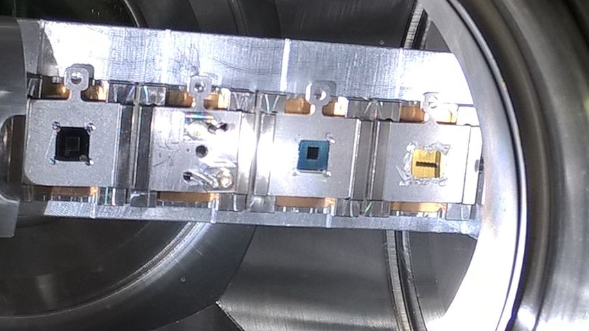
Milestones of WS development at PSI
SwissFEL wire-scanners (WS) with micrometer resolution:
innovative design on a footprint of a standard technique
Nano-fabricated WS with sub-micrometer resolution “on a membrane”
Simona Borrelli, Master thesis,Universita’ degli Studi di Pisa
“Free-standing” nano-fabricated WS with sub-micrometer resolution
Beam profile tomography with nano-fabricated WS,
Benedikt Hermann, PhD candidate, PSI and University of Bern
Nanofabricated WS at FERMI: similar development path pursued independently.
Fruitful collaboration between FERMI and PSI in the nano-fabricated WS project
Page 3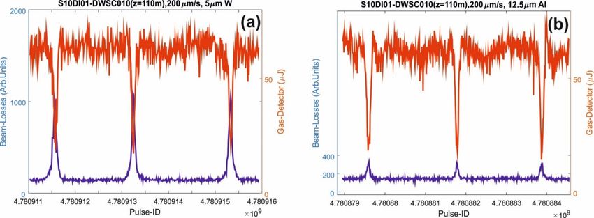
Presentation overview
WS in a FEL: brief introduction
Motivations and Goals of “WS nano-fabrication”
Nano-fabricated WS at PSI and FERMI: first developments
Nano-fabrication of free-standing sub-µm WS at PSI and FERMI
Free-standing sub-µm WS: experimental test at SwissFEL
Beam profile tomography with nano-fabricated WS
Conclusions and Outlook
Page 4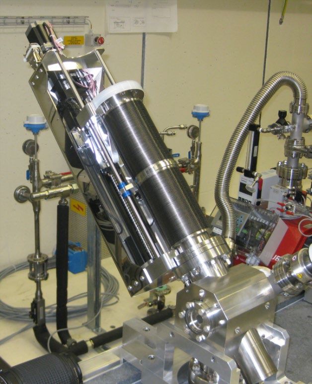
WS in a FEL: brief introduction (1/3)
Diagnostics of the beam transverse profile
Beam-probe: travelling wire (typically metal) sampling the beam transverse profile at every RF shot
Probe-signal (“wire-signal”):
e.m. shower (e-,e+,photons…) produced by the wire partially detected by a beam-loss-monitor (BLM)
BLM signal proportional to the number of particles sampled by the wire at every RF shot
Profile reconstruction: beam synchronous correlation of BLM signal and encoder readout of wire position
Spatial resolution:
Beam charge and transverse position jitter (corrected by BPM readouts and magnetics optics in
between)
Encoder resolution
Mechanical vibration of the wire
Geometrical resolution (normally dominating): rms size of the wire width
Performance:
Multi-shot and 1-dimensional reconstruction of the beam profile
High resolution and minimally invasive diagnostics
Page 5
WS in a FEL: brief introduction (2/3)
e.m. shower (WS signal):
mainly composed by primary scattered e- and secondary emitted particles (e+,e-,photons)
energy loss depending on:
Density and atomic number of the material
Wire width (w) determine wire impact surface number of primary scattered electrons
Wire thickness (t) determine:
o Amount energy loss (bremsstrahlung) per scattered electron
o Mean angular spreading per electron by multiple Coulomb scattering
o Minimize t improve matching of scattered beam with machine energy and angular acceptance
Design goal of WS in a FEL:
Minimize w and tw:
High geometrical resolution
Minimal invasiveness to the beam (machine
protection)
High transparency to the lasing
wire material with low density and atomic number…
…but adequate signal-to-noise ratio of BLM needed…
…then optimize thickness (t) to possibly compensate
Page 6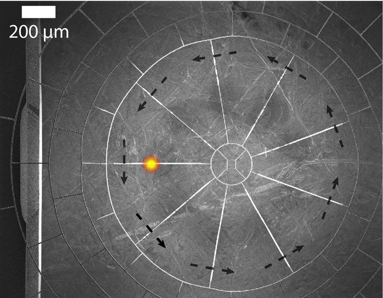
WS in a FEL: brief introduction (3/3)

WS signal in a FEL (e.g., SwissFEL): energy loss detected by BLM

                                                                   Page 7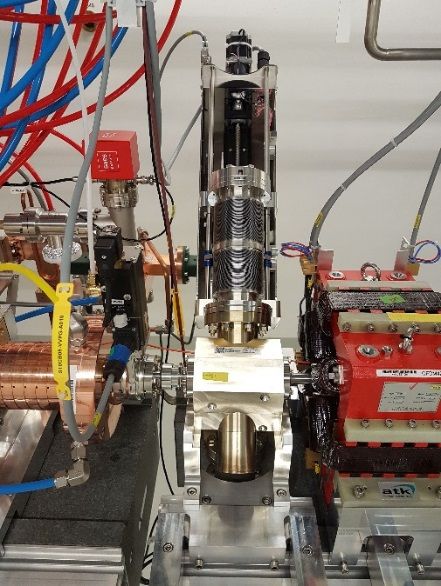
Conventional WS: resolution and invasiveness constraints (1/3)
SwissFEL WS:
Conventional WS design (metallic wire stretched onto a fork)
~20 WS installed all along the machine for beam profile monitoring and emittance measurements
Fork equipped with 2 pairs of wires (5 µm W and 12.5 µm Al(99):Si(1) wires)
SwissFEL, WS-relevant parameters: 200/10 pC, 0.300-5.8 GeV, beam-size 5-500 µm (rms)
Geometrical resolution (5 µm W wire): 1.25 µm
Beam profile reconstruction: beam synchronous acquisition of encoder position and BLM signal
BLM: scintillator fiber+POF+PMT
BLM: scintillator fiber
• License Agreement between PSI
and UHV-Design Ltd. for the
commercialization of the vacuum
chamber+wire fork.
• Motorized feedthrough produced
by UHV-Design
Page 8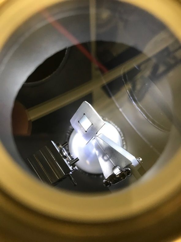
Conventional WS: resolution and invasiveness constraints (2/3)
Beam profile measurements at SwissFEL
Beam charge 10 pC, beam energy after BC1 ~300MeV, BC2~5.8 GeV
Beam energy 300 MeV, charge 20 pC, rep.rate 10Hz
5 µm W wire: scan_X (b) ; scan_Y (d) After BC1 After BC2
12.5 µm Al(99):Si(1) wire: scan_X (a) ; scan_Y (c) 300
Wire-scanner (data)
100
Wire-scanner (data)
Wire-scanner (fit) Wire-scanner (fit)
250
Screen (data) 80 Screen (data)
Screen (fit) Screen (fit)
m)
m)
200 Screen resolution
60
corrected
150
Beam size (
Beam size (
40
100
20
50
0 0
0 50 100 150 0 50 100 150
Phase advance (deg.) Phase advance (deg.)
Emittance measurements at SwissFEL: WS vs YAG screen,
E.Prat et al., Generation and Characterization of Intense Ultralow-
Emittance Electron Beams for Compact X-Ray Free-Electron Lasers,
PHYSICAL REVIEW LETTERS 123, 234801 (2019),
G.L. Orlandi et al, First experimental results of the commissioning of the SwissFEL wire-scanners, IBIC2017, Grand Rapids. Mi, USA
Page 9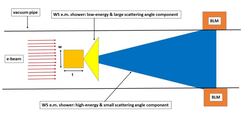
Conventional WS: resolution and invasiveness constraints (3/3)
Simultaneous WS and laser pulse energy measurements with gas detector (*):
Scan electron beam with 5µm W wire and 12.5µm Al(99):Si(1) wire and, in parallel, measure laser pulse energy
Al(99):Si(1) vs W wire beam-loss reduction by a factor 3-4 (beneficial to machine protection)
Al(99):Si(1) vs W wire despite lower density and atomic number, larger impact surface detrimental to lasing transparency
Higher WS geometrical resolution of the wire better wire transparency to the lasing
Energy (dE) radiated by single electron
with energy E in a thickness dX of matter
with radiation length LR
Beam-synchronous measurements of laser pulse energy (Gas-Detector) and e-beam profile (WS):
(a) 5 µm W wire;
(b) 12.5 µm Al(99):Si(1) wire.
Bunch charge ~200 pC, beam energy ~300 MeV at the WS location, 2.6 GeV at the undulator beamline, photon
energy 2.488 keV (wavelength=4.983A) .
(*) P. Juranic, et al., SwissFEL Aramis beamline photon diagnostics,J. Synchrotron Rad. (2018). 25, 1238-1248.
Page 10invasiveness
Motivations and Goals of “WS nano-fabrication”
Diagnostics with sub-µm resolution and minimally invasiveness needed for:
• Low-charge and low emittance beam and monitoring FEL operations
• Novel laser and plasma driven accelerator
Conventional WS (cylindrical metallic wires stretched onto a fork): spatial resolution limit ~1µm (rms)
Improve WS spatial resolution thinner wire smaller number of perturbed electrons
minimal beam invasiveness and higher transparency to lasing
New techniques to fabricate WS with resolution beyond the 1 µm (rms) limit
Nano-lithography (integration wire+fork in a unique structure)
Present status, free-standing WS independently nano-fabricated at PSI and FERMI and tested at SwissFEL:
• sub-µm spatial resolution (~250 nm)
• beam clearance ~2mm
Future plans:
• nano-fabricated free-standing WS with sub-µm resolution and beam clearance ~10mm
• free-standing sub-um wires (X,Y scan) integrated into a fork as a standard WS solution for a FEL.
Page 11First nano-fabricated WS at PSI: WS on-a-membrane with sub-µm resolution
WS nano-fabrication at Laboratory for Micro- and Nanotechnology (LMN, PSI):
(a) Si3N4 membrane + Cr-Au-Cr coating + PMMA resist spin-coating
(b) e-beam lithography of PMMA to write parallel stripes (isopropanol+water treatment to develop exposed resist)
(c) Developed membrane trenches filled with Au by electroplating (PMMA resist removed by oxygen-plasma)
Page 12Sub-µm WS on-a-membrane: e-beam test at SwissFEL (*)
Low charge and emittance machine setting: 330MeV,First nano-fabricated WS at FERMI-IOM-CNR: free-standing WS (*)
Free-standing WS nano-fabricated
by IOM-CNR and tested at FERMI:
geometrical resolution 2.9 µm
(*) M. Veronese, S. Grulja, G. Penco, M. Ferianis, L.
Froehlich, S. Dal Zilio, S. Greco, M. Lazzarino,
A nanofabricated wirescanner with free standing
wires: Design, fabrication and experimental results,
NIM A, 891, 32-36 (2018).
Page 14Free-standing nano-fabricated WS (IOM-CNR): e-beam test at FERMI
Page 15PSI and FERMI nano-fabricated free-standing WS
PSI WS chip: bulk Au stripe; width 800nm and FERMI WS chip: sandwich Au/Si3N4/Au;
500nm; thickness ~2µm thickness ~3µm [Au(1µm),Si3N4(2µm),Ti(20nm)]
6mm
Bulk Au vs sandwich Au/Si3N4/Au:
• Higher signal-to-noise ratio (see WS measurement slide)
• Possible minor mechanical stability when increasing the beam clearance
Page 16SEM images of the nano-fabricated WS structures
~900nm
~700nm
~800um
~2mm
PSI WS nano-fabrication, FERMI WSC nano-fabrication,
Laboratory for Micro- and Nanotechnology, LMN, PSI IOM-CNR, Trieste, Italy
Page 17Experimental set-up at SwissFEL
beam vertical size at the
WS position: ~500nm
βx, βy evolution between BC1 and WS sub-µm
Page 18Sub-um WS set-up in the sample holder of the “ACHIP” vacuum-chamber
PSI >1µm
5um W wire
(reference)
WS chips mounted on a 4-slot sample
holder.
PSIFree-standing sub-µm WS: experimental test at SwissFEL (*)
Beam profiles acquired with PSI (1) and FERMI (2) WS
in two different measurement sessions (a, b):
• low-charge (Beam Profile Diagnostics with Nanofabricated Wire Scanner -
Tomography
• 9 Gold wires oriented at different angles
• Wire width: 1 μm
• Free-standing spider web
• Fabricated at PSI by Laboratory for Micro-
and Nanotechnology with e-Beam
lithography
• Measure 1D beam projections with
downstream loss monitor
• 4D Beam tomography:
B. Hermann et al, 2021, PRAB
https://doi.org/10.1103/PhysRevAccelBeams.24.022802
Page 21Beam Profile Diagnostics with Nanofabricated Wire Scanner -
Tomography
Charge: 10 pC, Energy: 3 GeV
B. Hermann et al, 2021, PRAB
https://doi.org/10.1103/PhysRevAccelBeams.24.022802
Page 22Wire Scanner Reconstruction vs.
50 μm Thick YAG Screen + Microscope
Same machine settings for WSR and YAG measurement, charge: 1 pC.
Page 23Conclusions and Outlook Innovative free-standing WS structure with unprecedented sub-micrometer geometrical resolution (~250nm). Nano-fabrication by LMN at PSI and byIOM-CNR for FERMI. Successful experimental tests at SwissFEL of FERMI and PSI free-standing WS at low charge (
Wir schaffen Wissen – heute für morgen

                    Thank you for your attention

                                                   Page 25
You can also read


