Novel Bandwidth Expander Supported Power Amplifier for Wideband Ultrasound Transducer Devices - MDPI
←
→
Page content transcription
If your browser does not render page correctly, please read the page content below
sensors
Article
Novel Bandwidth Expander Supported Power Amplifier for
Wideband Ultrasound Transducer Devices
Kyeongjin Kim and Hojong Choi *

                                          Department of Medical IT Convergence Engineering, Kumoh National Institute of Technology,
                                          350-27 Gumi-daero, Gumi 39253, Korea; 20196092@kumoh.ac.kr
                                          * Correspondence: hojongch@kumoh.ac.kr; Tel.: +82-054-478-7782

                                          Abstract: Ultrasound transducer devices have their own frequency ranges, depending on the appli-
                                          cations and specifications, due to penetration depth, sensitivity, and image resolution. For imaging
                                          applications, in particular, the transducer devices are preferable to have a wide bandwidth due to the
                                          specific information generated by the tissue or blood vessel structures. To support these ultrasound
                                          transducer devices, ultrasound power amplifier hardware with a wide bandwidth can improve the
                                          transducer performance. Therefore, we developed a new bandwidth expander circuit using specially
                                          designed switching architectures to increase the power amplifier bandwidth. The measured band-
                                          width of the power amplifier with the help of the bandwidth expander circuit increased by 56.9%.
                                          In addition, the measured echo bandwidths of the 15-, 20-, and 25-MHz transducer devices were
                                          increased by 8.1%, 6.0%, and 9.8%, respectively, with the help of the designed bandwidth expander
                                          circuit. Therefore, the designed architecture could help an ultrasound system hardware with a wider
                                          bandwidth, thus supporting the use of different frequency ultrasound transducer devices with a
                                          single developed ultrasound system.


                                          Keywords: bandwidth expander; ultrasound transducer device; power amplifier
Citation: Kim, K.; Choi, H. Novel
Bandwidth Expander Supported
Power Amplifier for Wideband
Ultrasound Transducer Devices.            1. Introduction
Sensors 2021, 21, 2356. https://
doi.org/10.3390/s21072356
                                               Ultrasound transducers are the main sensor devices used in ultrasound systems [1].
                                          Different types of ultrasound transducers are used, depending on their applications and
Academic Editor: Changho Lee
                                          specifications [2]. Engineers have manufactured ultrasound transducers with the required
                                          diagnostic applications. For diagnostic applications with different positions and locations,
Received: 17 February 2021                the imaging resolution and sensitivity performance are merits in the evaluation of ul-
Accepted: 25 March 2021                   trasound systems [3]. Typically, lower-frequency ultrasound transducer devices have a
Published: 28 March 2021                  higher penetration depth and lower imaging resolution than higher-frequency ultrasound
                                          transducer devices [4]. Smaller-sized ultrasound transducer devices for intracardiac and
Publisher’s Note: MDPI stays neutral      intravascular applications need to be used such that the penetration depth of the devices is
with regard to jurisdictional claims in   lower, but a higher imaging resolution could be preferable [5].
published maps and institutional affil-        Figure 1 shows the penetration depth and imaging resolution for an ultrasound
iations.                                  diagnostic analysis. Since the imaging resolution and penetration depth have a trade-
                                          off relationship, ultrasound transducers with smaller piezoelectric elements are used
                                          depending on the body parts [6]. For the heart and abdomen areas, 2–3 and 3–5 MHz
                                          transducer devices are preferable because of the penetration depth [5,7]. For the eyeballs
Copyright: © 2021 by the authors.         and breast and thyroid areas, 7.5–12 MHz and 7.5–13 MHz transducer devices are used
Licensee MDPI, Basel, Switzerland.        due to their relatively high imaging resolutions [5,7]. In particular, for peripheral blood
This article is an open access article    vessels and digestive tract areas, small transducer devices with a high frequency, such
distributed under the terms and           as 15–30 MHz, are used because of the higher imaging resolution, which reduces the
conditions of the Creative Commons        penetration depth [8–10].
Attribution (CC BY) license (https://
creativecommons.org/licenses/by/
4.0/).

Sensors 2021, 21, 2356. https://doi.org/10.3390/s21072356                                                 https://www.mdpi.com/journal/sensors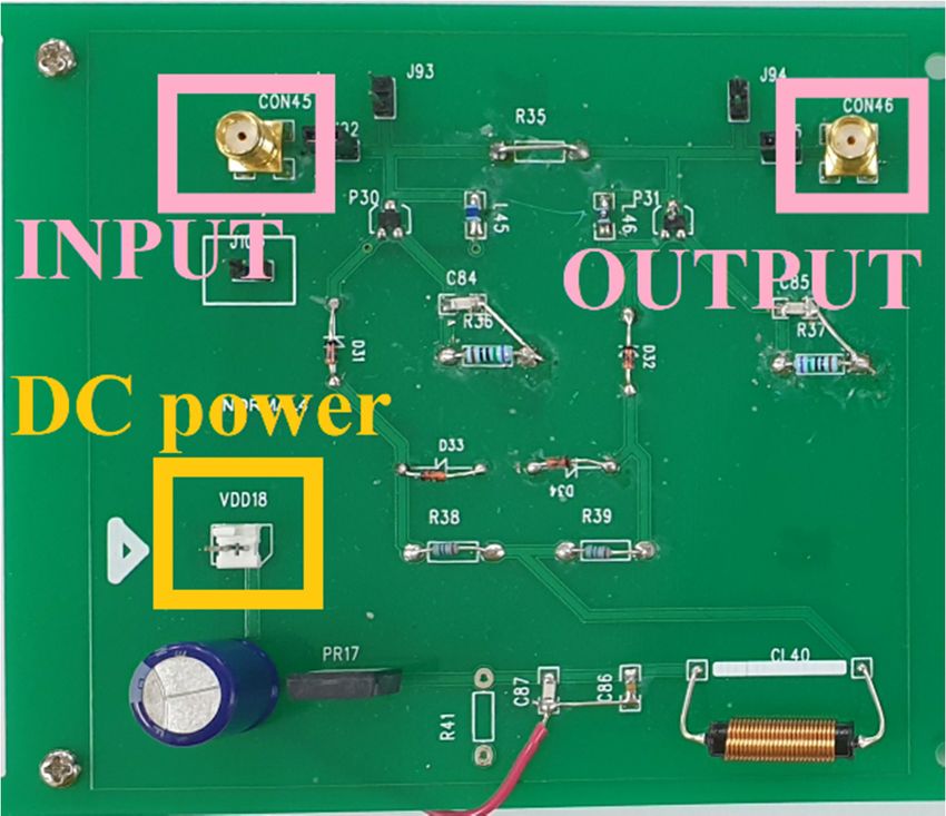
Sensors 2021, 21, x FOR PEER REVIEW 2 of 19
Sensors
Sensors 2021, 2021,
21, 235621, x FOR PEER REVIEW 2 of 19 2 of 18
Figure1.1.Penetration
Figure Penetrationdepth
depthand
andimaging
imagingresolution
resolutionfor
forultrasound
ultrasounddiagnostic
diagnosticanalysis.
analysis.
Figure 1. Penetration depth and imaging resolution for ultrasound diagnostic analysis.
Figure22shows
Figure showsthetheultrasound
ultrasoundtransducer
transducerprobes
probes(devices)
(devices)used
usedininultrasound
ultrasoundsys-sys-
tems
tems forfor specific
specific
Figure applications
applications
2 shows [7,11].
[7,11].
the ultrasound Each ultrasound
Each ultrasound
transducer transducer
transducer
probes (devices) probe
used in probe has different
has sys-
ultrasound fre-
different
quency
frequency characteristics
tems for characteristics and
andshapes;
specific applications [7,11].
shapes; thus,
Each different
ultrasound
thus, anatomical
transducer
different anatomical cross-sectional
probe has differentimages
cross-sectional fre-
imagesare
obtained
are quency
obtained [11,12]. However,
characteristics
[11,12]. only
onlyone
and shapes;
However, oneultrasound
thus, system
system may
different anatomical
ultrasound coverimages
cross-sectional
not cover thetransducer
the transducer
are
obtained
probes
probes with[11,12].
with However,
different
different onlyranges.
frequency
frequency one ultrasound system may not cover the transducer
ranges.
probes with different frequency ranges.
Figure 2. Transducer devices for various applications.
Figure2.2.Transducer
Figure Transducerdevicesdevicesfor forvarious
variousapplications.
applications.
Various classes of power amplifiers have been developed for different types of ultra-
Various
sound
Various classes
transducer
classes ofofpower
devices.
powerIn amplifiers
power have
havebeen
amplifiers,
amplifiers the
been developed
input signals are
developed for different
differenttypes
foramplified by ofofultra-
active
types ultra-
sound transducer
devices, which wedevices.
call In power amplifiers,
metal-oxide-semiconductor the input
field-effect
sound transducer devices. In power amplifiers, the input signals are amplified by signals are
transistors amplified
(MOSFETs) byoractive
active
devices,
devices, which
whichwe
lateral-diffusion we call
callmetal-oxide-semiconductor
metal–oxide semiconductors (LDMOSs)
metal-oxide-semiconductor field-effect transistors
[13]. Depending
field-effect transistors (MOSFETs)
on the direct
(MOSFETs) oror
current (DC) bias
lateral-diffusion voltages, thesemiconductors
metal–oxide output currents generated
(LDMOSs) by [13].
the active devices are
Depending on fully
the direct
lateral-diffusion metal–oxide semiconductors (LDMOSs) [13]. Depending on the direct
or partially
current (DC) bias conducted
voltages,duringthe aoutput
single period
currents of generated
time [14]. This fundamental
by the active devicesconceptare is fully
current (DC) bias voltages,
used to categorize power
the output
amplifier
currents
classes,
generated
suchofastime classes
by the active devices are fully
or partially conducted during a single period [14].A,This
B, and C. In the Class
fundamental A
concept is
orpower
partially conducted
amplifier, the duringbias
operating a single period of time the[14]. This of fundamental concept is
used to categorize power amplifiervoltage is located
classes, such asinclasses middleA, B, the
andDC C.load line
In the to
Class A
used to categorize
minimize power amplifier
signal distortions classes,
[15]. Therefore, such as
the active classes
device A,power
in the B, and C. In the
amplifier has Class
a A
power amplifier, the operating bias voltage is located in the middle of the DC load line
power
heavyamplifier,
load because thetheoperating bias voltage
active device continuesis tolocated
operate inregardless
the middle of of
thethe DCsignal
input load line to
to minimize signal distortions [15]. Therefore, the active device in the power amplifier
minimize signalisdistortions
[16,17]. Power [15]. Therefore,
consumed continuously the as
as long active device
an active in the
device is power
operating. amplifier
How- has a
hasever,
a heavy load
signalbecause
because
distortion
the active
byactive
an active
device
device
continuesresulting
is minimized,
to operate regardless
in an output
of with
the input
heavy load the device continues to operate regardless ofsignal
the input signal
signal [16,17].
high linearity Power is consumed continuously as long as an active device is operating.
[16,17]. Power [18]. In Class B power
is consumed amplifiers,
continuously as the
long bias
asvoltage
an activeis located
device near the middle How-
is operating.
However,
of the DCsignal
load distortion
line, and by an active device isoperates
minimized, resulting in an output thesignal
ever, signal distortion by thus,
an activethe active
device device
is minimized, only for
resulting halfinthe
an period
outputofsignal with
with high linearity [18]. In Class B power amplifiers, the bias voltage
signal [17]. Therefore, the active device operates for only half a period, which causes signal is located near the
high linearity [18]. In Class B power amplifiers, the bias voltage is located near the middle
middle of thealthough
distortion, DC loadthe line, and consumption
power thus, the active of the device
activeoperates
device is only for half
reduced, the period
compared to of
of the DC load line, and thus, the active device operates
the signal [17]. Therefore, the active device operates for only half a period, which causes
that of the Class A power amplifier. Class C power amplifiers
only
operate
for half
for less
the
than
period
half a
of the
signaldistortion,
signal [17]. Therefore, the active
although deviceconsumption
the power operates for only half
of the a period,
active devicewhich causes signal
is reduced, com-
distortion, although the power consumption of the active device is reduced,
pared to that of the Class A power amplifier. Class C power amplifiers operate for compared
less thanto
thata of
half the Class
period of theAsignal
powerbecause
amplifier.
the Class C power
bias voltage amplifiers
of the DC loadoperate for less
line is lower than
than half
that of a
Class B amplifiers [13]. Therefore, the distortion of the signal is extremely high, whereas
the power consumption of the active device is quite low. In addition, Class AB power
amplifiers operate between Class A and B power amplifiers. In addition, there are other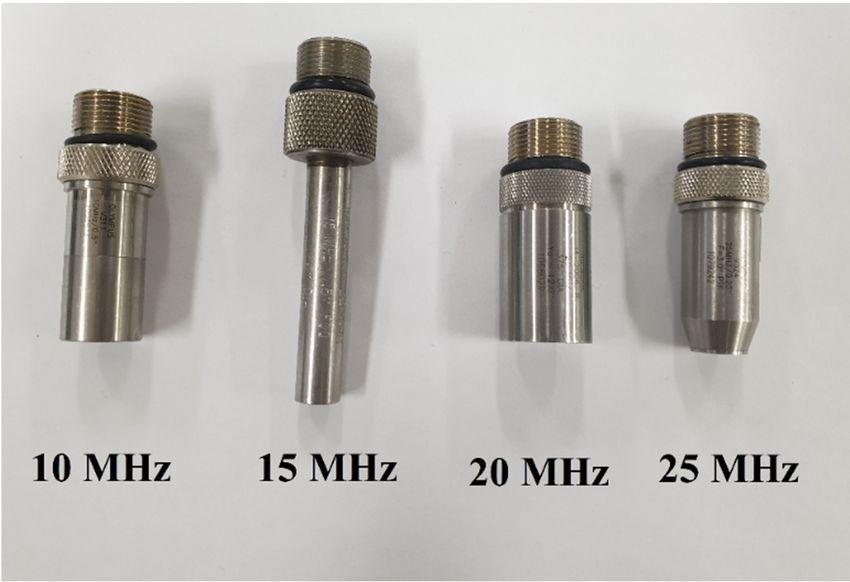
Sensors 2021, 21, 2356                                                                                          3 of 18

                         types of power amplifiers, such as Class D and Class E, which use harmonic components
                         or modulated waveforms [19].
                               The Class B power amplifiers operate at only half of the pulse cycle, which has a
                         much shorter time than Class A and Class AB power amplifiers. Therefore, Class B power
                         amplifiers have much lower power consumption than those of Class A and Class AB power
                         amplifiers, and thus, they have a higher efficiency [20]. The Class B power amplifier has
                         lower signal distortions than the Class A power amplifier. Therefore, wire-type ultrasound
                         machines have a Class A power amplifier because of the AC power cord [2]. Class B or
                         Class C power amplifiers are preferable for mobile or portable ultrasound systems due
                         to their limited battery modules [6]. Several studies related to power amplifiers have
                         been conducted on ultrasound-transducer devices. For ultrasound signals, the burst or
                         modulated waveforms with a limited time period and non-continuous signals are used. A
                         typical Class A power amplifier was developed for ultrasound imaging applications [21].
                         A Class B power amplifier was developed to reduce the signal distortion [22].
                               There are a few studies of the power amplifiers used for ultrasound applications.
                         There is a Class C power amplifier used for a 25 MHz transducer. This amplifier has high
                         efficiency with high signal distortions. Therefore, the proposed circuit was developed to
                         compensate for signal distortions [23]. Class D amplifier was developed for low-frequency
                         piezoelectric transducers [24]. This amplifier was used for the high signal distortion
                         and high-efficiency system. The Class E power amplifier was developed to improve the
                         efficiency of low-frequency inductive piezoelectric converters [25]. As mentioned, various
                         power amplifiers with various characteristics are used because all the amplifiers cannot
                         satisfy some parameters of the signal distortion and the bandwidth. In ultrasound systems,
                         transmitter and receiver architectures support ultrasound devices. The power amplifier in
                         a transmitter is typically used in the last stage of electronics [2]. Thus, the bandwidth of
                         the power amplifier only covers the specific transducer probes with their limited frequency
                         ranges because the bandwidth of the power amplifier electronic devices decreases as
                         the operating frequency of the power amplifier increases. This indicates that the output
                         signals working at frequencies higher than the center frequency may deteriorate the image
                         quality. Therefore, we first proposed a bandwidth-expander circuit for power amplifiers
                         and various ultrasound devices.
                               There are several ways to increase the bandwidth of the power amplifier output.
                         Impedance matching improves the amplitude and bandwidth of the power amplifiers
                         and ultrasound transducers [26]. The output power can be increased through impedance
                         matching, thus increasing the echo amplitude or the echo bandwidth of the ultrasound
                         transducers [26]. However, the impedance of the ultrasound transducer varies significantly
                         according to the frequency [27]. Furthermore, transducers are manufactured to have differ-
                         ent central frequencies and resonance/anti-resonance frequency ranges [28]. Therefore, it
                         can be difficult to match the impedance magnitudes within the desired frequency ranges
                         for several ultrasound transducers.
                               Another method is to lower the gain and increase the bandwidth of the power amplifier
                         by using a feedback loop circuit [14]. This method a fundamental approach for increasing
                         the bandwidth of a power amplifier. This method can reduce the gain of the power
                         amplifier and increase the bandwidth [16]. Thus, several-stage power amplifiers need to be
                         utilized to increase the gain and bandwidth. As the number of stages increases, various
                         problems such as a time delay and signal distortions due to line resistances and parasitic
                         nonlinear components could affect the performance of the power amplifiers [29]. Moreover,
                         there could be a bandwidth expansion limit because space and cost are finite in terms
                         of manufacturing.
                               In this study, we developed a circuit that can enlarge the bandwidth and minimize
                         the signal loss, thus applying it to a single-stage power amplifier. In our proposed circuit,
                         the bandwidth can be improved by lowering the input poles of the power amplifiers. The
                         designed circuit works as a switching mode that is simply turned on/off with DC power.
                         This method can be useful to improve the bandwidth of the power amplifier and minimize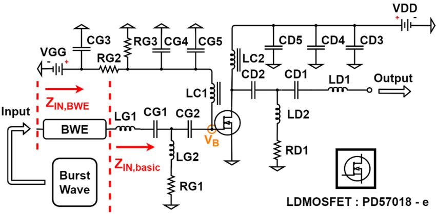
Sensors 2021, 21, 2356                                                                                          4 of 18

                         the signal loss, thus supporting higher-frequency ultrasound devices. Section 2 describes
                         the theoretical background and analysis of the proposed circuit and the power amplifier.
                         Section 3 presents the measured performance and a discussion of the proposed circuit with
                         several ultrasound transducers. Section 4 provides some concluding remarks regarding
                         this research.

                         2. Materials and Methods
                               The designed bandwidth expander (BWE) is a type of switching circuit operated by
                         different applied DCs. It is located before the lateral-diffusion metal-oxide-semiconductor
                         field-effect transistor (PD57018-E, LDMOSFET, STMicroelec-tronics, Geneva, Switzerland),
                         which is a type of high-voltage MOSFET (BSS123, active device in BWE) in the input
                         port of the amplifier. When the active LDMOSFET device in the amplifier operates under
                         higher-voltage amplitudes than a certain bias voltage, the amplifier is applied to the gate
                         of the LDMOSFET [30]. Therefore, the drain and source of the MOSFET are applied such
                         that the input impedance of the amplifier is changed accordingly. In addition, by adjusting
                         the input impedance, the input poles of the amplifier can be tuned. The total transfer
                         function of the amplifier is expected to increase by integrating the BWE circuit with the
                         amplifier. Therefore, the amplifier with the help of the BWE has a higher output amplitude
                         and wider bandwidth.

                         2.1. Designed Power Amplifier and BWE Schematic Diagram
                               Figure 3 shows an amplifier combined with a BWE circuit for the ultrasound trans-
                         mitter. Table 1 shows the resistor, capacitor, and inductor elements of the amplifier, except
                         for the LDMOSFET shown in Figure 3. The LDMOSFET (PD57018-E, STMicroelectronics,
                         Geneva, Switzerland) was used as the core component of the amplifier. The simulation
                         was conducted to make the impedance matching suitable for the 15 MHz transducer. In
                         Figure 3, VB is the main gate-source operating point of the LDMOSFET. In addition, LC1
                         and LC2 are choke coil inductors that prevent the inflow of the alternating current (AC)
                         into the DC power supply [31]. The components used in the input line (LG1, LG2, CG1,
                         CG2, and RG1) and the components used in the output line (LD1, LD2, CD1, CD2, and
                         RD1) are tuned to be compatible with the 15 MHz transducer and to achieve the values
                         below −10 dB of S (1,1) and S (2,2). In addition, they need to block the DC current from
                         VGG and VDD using CG2 and CD2. If AC input voltages enter the DC power supply,
                         oscillations may occur [32]. The polarizing electrolytic capacitors CG3 and CD2 are helpful
                         in providing a constant direct voltage [33]. The ceramic capacitors CG4, CG5, CD4, and
                         CD5 were used to reduce noise as bypass capacitors. The bias voltage was adjusted to
                         operate through the voltage distributions of RG2 and RG3. The bias voltage equation at VB
                         is as follows [34,35]:
                                                                             RG3
                                                          VB = VGG ×                 .                             (1)
                                                                          RG2 + RG3

                         Table 1. Numerical values of the circuit elements of Figure 3.

                              Components                   Values                Components           Values
                                   RG1                    200 ohm                    CD2               850 µF
                                   RG2                   1000 ohm                    CD3               220 µF
                                   RG3               Variable resistance             CD4              1000 pF
                                   RD1                    200 ohm                    CD5               100 pF
                                   CG1                     550 pF                    LG1               21 nH
                                   CG2                     340 pF                    LG2              1000 nH
                                   CG3                     220 µF                    LD1              130 nH
                                   CG4                    1000 pF                    LD2              500 nH
                                   CG5                     100 pF                    LC1                1 µH
                                   CD1                     340 pF                    LC2                1 µH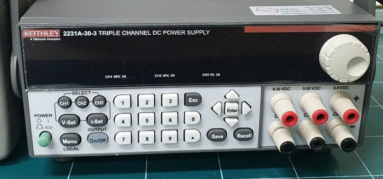
Sensors 2021, 21, x FOR PEER REVIEW 5 of 19
Sensors 2021, 21, 2356 5 of 18
the output amplitude and bandwidth are changed. This concept is proved through several
equations.
Figure 3. Designed amplifier schematic diagram.
Figure 3. Designed amplifier schematic diagram.
In ultrasonic diagnostic equipment, the frequency of the input signal and the cycle
of the1.burst
Table wave values
Numerical were adjusted such
of the circuit that theofQFigure
elements factor3.used for providing an appropriate
image quality was calculated [1]. Assuming that the LDMOSFET operates in the saturation
Components Values Components Values
region, the changes in the pole and transfer function can be estimated. As shown in Figure 3,
the BWE circuit has little effect on the impedance. However, if a DC voltage850
RG1 200 ohm CD2 µF
is applied and
operated,RG2 the input impedance 1000changes.
ohm Therefore, the CD3 input pole changes. 220 AsµFthe input
RG3 the transfer
pole is varied, Variable
functionresistance
according to the CD4 frequency changes, and 1000the pF output
RD1 200 ohm CD5
amplitude and bandwidth are changed. This concept is proved through several equations. 100 pF
CG1
Figure 4 shows a schematic 550diagram
pF of the designed LG1BWE to show the circuit 21 nH element
values. CG2Table 2 shows the numerical 340 pF values of the LG2 resistors, capacitors, 1000andnH inductor
elementsCG3in Figure 4. R1 and R3 were
220 µF used to be tuned to
LD1 have proper voltage130 nHdistribution
and power CG4 consumption because 1000M1 pF needs to be operated LD2 properly. The input 500 nH signal was
connected CG5to the gate of M1 to form
100 pF a feedback loop and can
LC1 cause oscillation 1 µH blocked
to be
through CD1
L1. However, the too340 high
pF value of inductance LC2 may distort the input
1 µHsignal, so
we properly selected the inductor value. R2 and C1 play a major role to lower the input
Figure 4because
impedance shows athe schematic
drain and diagram
sourceofoftheM1designed BWEIftothe
are shorted. show the circuit
impedance is element
too low,
values. Table 2 shows
signal amplitude thereduced.
can be numerical values
Thus, weofproperly
the resistors,
selectedcapacitors, and inductor
those values for an inputele-
ments
signal in
of Figure
15 MHz. 4. R1 and
This R3 were
circuit usedto
is added tothe
be circuit,
tuned to ashave
shown proper voltage
in Figure 3, anddistribution
thus the
amplifier
and powerperformance
consumptionbybecause
applying M1different
needs toconstant
be operatedDC voltages
properly.isThe changed
input depending
signal was
on the MOSFET
connected to the (M1, BSS123)
gate of M1 to operation. Whenloop
form a feedback this circuit
and canis cause
assumed to be antoideal
oscillation current
be blocked
source or ideal
through L1. However,switch, the DC bias voltage V
too high value of inductance
B1 in the BWE circuit operates the
may distort the input signal, so transistor,
M1,properly
we as described below
selected the[36–38]:
inductor value. R2 and C1 play a major role to lower the input
impedance because thedrain and source of M1 are shorted. If the impedance is too low,
R2 || R2
signal amplitudeVcan B1 =be Vreduced.
DC − V Thus,
D1( TH ) −we
V SDproperly
× selected those values, for an input (2)
R + R2 || R2 + R3 || R3
signal of 15 MHz. This circuit is added to the circuit,1 as shown in Figure 3, and thus the
amplifier performance
where VD1(TH) and VSDby areapplying different
the threshold constant
voltage DC voltages diode
and drain-source is changed
forward depending
voltage,
on the MOSFET (M1, BSS123) operation. When this circuit is
respectively. Above a certain voltage, VB1 shortens the drain and source of M1. assumed to be an idealAscur-
the
rent source or ideal switch, the DC bias voltage V B1 in the BWE circuit
drain and source voltages at M1 are short-circuited, C1, R2, and L1, and the capacitance operates the tran-
sistor, M1, as resistance
and on-state described inside
below M1 [36–38]:
are connected in parallel to the input impedance.
||
= − ( ) − × , (2)
+ | + |
ors 2021, 21, x FOR PEER REVIEW 6 of 19
where VD1(TH) and VSD are the threshold voltage and drain-source diode forward voltage,
Sensors 2021, 21, 2356 respectively. Above a certain voltage, VB1 shortens the drain and source of M1. As the 6 of 18
drain and source voltages at M1 are short-circuited, C1, R2, and L1, and the capacitance
and on-state resistance inside M1 are connected in parallel to the input impedance.
Figure 4. Schematic diagram of designed bandwidth expander (BWE) circuit.
Figure 4. Schematic diagram of designed bandwidth expander (BWE) circuit.
Numerical
Table 2.values
Table 2. Numerical of the values
circuit of the circuit
elements elements
of Figure 4. of Figure 4.
Components Components
Values Values
Components Components
Values Values
R1 150 R1
ohm C3ohm
150 C3 1000 pF 1000 pF
R2 R2
750 ohm 750
C4ohm C4 100 pF 100 pF
R3 50 ohm L1 560 nH
R3 50 ohm L1 560 nH
C1 47 pF L2 1 µH
C1 47C2
pF L2
220 µF 1 µH
C2 220 µF
2.2. Predicting Performance Results
2.2. Predicting Performance Results
Changes in the performance of the amplifier only and the amplifier with BWE can
Changes bein the performance
expected and comparedof the amplifier
based on only
pole and the amplifier
calculations. with BWE
Therefore, the can be
equivalent circuit
expected and compared based on pole calculations. Therefore, the equivalent
models of the LDMOSFET in the amplifier and the MOSFET in the BWE were simplifiedcircuit mod-
els of the LDMOSFET
to calculatein
thethe amplifier
poles. andinput
First, the the MOSFET
impedance in the
(ZINBWE
,basic ) were
of thesimplified to
amplifier (Figure 5) was
calculate thecalculated
poles. First, the input
as follows: impedance (ZIN,basic) of the amplifier (Figure 5) was cal-
culated as follows:
Z I N,basic = XCG2 ( X LG2 + RG1) + XCG1 + X LG1 , (3)
, = ||( + 1) + + , (3)
where
where XCG1 and XCG1
XCG2 are the XCG2 are theofimpedances
andimpedances of the
the capacitors, andcapacitors,
XLG1 is theand XLG1 is of
impedance thethe
impedance of
theFigure
inductor (see inductor5). (see
When Figure
the V5).
DCWhen the VDC
is applied is applied
to M1, the VPPto of
M1, the VPP of
theinput the input
signal is signal is
blocked
blocked at D1 becauseat D1
the because
DC levelthe DC level isbyincreased
is increased by VB1in, as
VB1, as shown shown
Figure in Figure
4. In addition,4. In addition,
the gate
the gate of M1 of M1 is short-circuited
is short-circuited due to the
due to the applied VDCapplied VDC . The
. The on-state on-stateRresistance
resistance D and RD and
internal capacitances
internal capacitances CGD, CGS, and CGD
CD, C GS , and
exist. WhenCD exist.
M1 inWhen
the BWE M1 in the BWE
circuit circuit
operates, it operates,
is it is
expressed as an equivalent circuit for the AC analysis.
expressed as an equivalent circuit for the AC analysis. Here, ZBWE indicates Here, Z indicates
the impedance
BWE the impedance
of thecircuit
of the equivalent equivalent
whencircuit whenoperates
the circuit the circuit operates
and and isasexpressed
is expressed follows: as follows:
=ZBWE|| =||R D X ||CD + X L1 XC+ R2||
GD
+ XCGS. + R2 XC1 . (4) (4)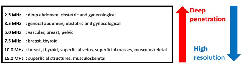
The input impedance in the BWE circuit was operated with parallel circuits, as shown
Sensors 2021, 21, x FOR PEER REVIEW 7 of 19
in Figure 5.
Sensors 2021, 21, 2356 , = | | , . (5)
7 of 18
The input impedance in the BWE circuit was operated with parallel circuits, as shown
in Figure 5.
, = | | , . (5)
Figure5.5.Equivalent
Figure Equivalentcircuit
circuitmodel
modelwhen
whenBWE
BWEcircuit
circuitisisoperated.
operated.
Figure
The input6 shows the equivalent
impedance in the BWEcircuit
circuitmodel of the amplifier
was operated [17]. circuits,
with parallel Assuming that the
as shown
inbias voltage
Figure 5. VB of the amplifier only, and the amplifier with BWE are assumed to be the
Figure
same, the 5. Equivalent
internal circuit
capacitances model when
CL,GD BWE
, CZL,GS circuit
, C||L,DS ||isZ
, and goperated.
mVgs are
Z I N, BWE = BWE ZBWE I N,basic . the same. (5)
Figure 6 shows
Figure the equivalent
6 shows circuit
the equivalent model
circuit of the
model of amplifier
the amplifier [17].[17].
Assuming that that
Assuming the the
biasbias
voltage V of the amplifier only, and the amplifier with BWE are assumed
voltage VB of the amplifier only, and the amplifier with BWE are assumed to be the
B to be the
same, the internal
same, capacitances
the internal CL,GD
capacitances , CL,GS
CL,GD , C,L,DS
, CL,GS CL,DS , andgmgmVVgsgs are
, and arethe
thesame.
same.
Figure 6. Equivalent circuit model of the amplifier.
As a result, the input and output poles and the transfer function can be predicted.
The input pole of the amplifier only and the amplifier with the BWE circuit are given by
Equation Figure
(6).
Figure 6. Equivalent
6. Equivalent circuit
circuit modelmodel ofamplifier.
of the the amplifier.
1
As aAs a result,
result, the input
the input and
,
and= output
output poles poles
andand the transfer
the transfer function
function can can be predicted.
be predicted.
(6)
The The input
input polepole of amplifier
of the the amplifier and, and
onlyonly [ the +
the amplifier (1 with
+ with
, amplifier the) BWE
the]BWE circuit
circuit are given
are given by by
Equation (6). (6).
Equation
1
ω I N,basic = 1 (6)
= [CL,GS + (1 + gm R D )CGD ]
, Z I N,basic (6)
, [ , + (1 + ) ]
1
ω I N,BWE = (7)
Z I N,BWE [CL,GS + (1 + gm R D )CGD ]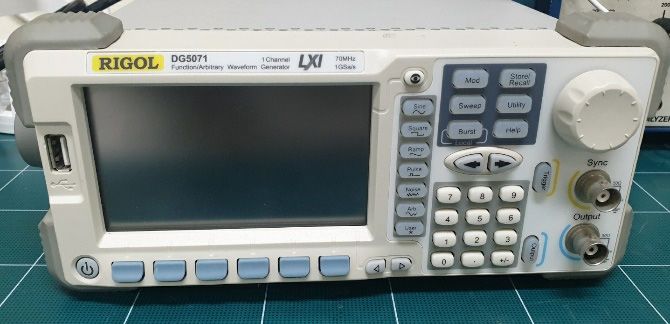
Sensors 2021, 21, 2356                                                                                             8 of 18

                               The output impedances of the amplifier only and the amplifier with the BWE circuit are
                         assumed to be the same. The currents flowing from drain to source in the main transistor
                         are the same if the same bias voltage is applied to both the amplifier and amplifier +
                         BWE; the internal capacitance (Ciss , Coss, and Crss ) is also the same. Thus, the internal
                         capacitances (CL,GD , CL,GS , CL,DS , and gm Vgs ) are supposed to be the same. Therefore, the
                         output impedances of the amplifier and amplifier + BWE are the same as ZOUT . Irrelevant
                         to a transducer, the output signal does not change. Consequently, the output poles in the
                         transfer functions of the amplifier only and the amplifier with the BWE circuit are expressed
                         in Equations (8)–(10).

                                                                  1                         1
                                       ωOUT =           h                      i ∼
                                                                                   =                                  (8)
                                                 ZOUT       CDS + 1 − A− 1
                                                                             CGD     ZOUT (CDS + CGD )
                                                                       v

                                                 VOUT                            − gm ZOUT
                                                       (s), basic =                                               (9)
                                                  VI N                1+          s
                                                                                            1+    s
                                                                             ω I N,basic         ωOUT

                                                VOUT                             − gm ZOUT
                                                      (s), BWE =                                                (10)
                                                 VI N              1+              s
                                                                                           1+      s
                                                                             ω I N, BWE          ωOUT

                              Equation (11) shows that ZIN,BWE has a relatively lower impedance than ZIN,basic
                         because ZBWE is connected in parallel to ZIN,basic . Looking at Equations (6) and (7), the input
                         pole has an inversely proportional relationship with the input impedance. Furthermore,
                         from Equations (9) and (10), the transfer function has a proportional relationship with
                         the input pole. As a result, the pole and transfer functions due to the different input
                         impedances can be predicted as follows:

                                                                Z I N,basic > Z I N,BWE                             (11)

                                                               ω I N,basic < ω I N,BWE                              (12)
                                                      VOUT               V
                                                            (s), basic < OUT (s), BWE.                              (13)
                                                       VI N               VI N
                              However, the predicted results should be operated in an ideal environment. The
                         actual results are extremely different from the predicted results because the high-voltage
                         amplifier operations are not accurately predictable due to several high-voltage environment
                         variables such as parasitic impedances, high-voltage valuable variances, and unpredictable
                         equivalent inductance models [39,40].
                              Figure 7 shows the predicted graph based on Equations (11)–(13). By adding a BWE
                         circuit to the existing amplifier, the magnitude and input pole in the transfer function
                         increase. In Figure 7, the entire line goes up, and the input pole moves to the right. As
                         a result, we assume that the line decreases by 20, 40, and 20 dB/dec, respectively, in the
                         interval between the input pole, the output pole, and the zero point. Comparing the two
                         cases, the transfer function is expected to increase. As the pole location shifts, we can
                         expect to achieve a wider bandwidth.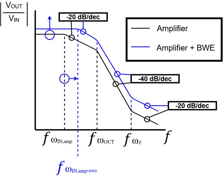
Sensors 2021,
Sensors 21,21,
2021, 2356
x FOR PEER REVIEW 9 of 1819
9 of
Figure 7. The predicted transfer function graph of the amplifier only and the amplifier with BWE.
Figure 7. The predicted transfer function graph of the amplifier only and the amplifier with BWE.
2.3. Experimental Measurement Process
2.3.Figure
Experimental
8 showsMeasurement Processshowing the performance measurement of the am-
a block diagram
plifier Figure
only and8 shows a block with
the amplifier diagram
BWEshowing
circuits. the performance
A function measurement
generator, DC power ofsupply,
the am-
plifier only
attenuator, andand the amplifier
oscilloscope with
were usedBWE circuits. the
to measure A function
performancegenerator,
of the DC powercircuits.
designed supply,
Aattenuator,
BWE circuitandwasoscilloscope were used
installed between to measure
the function the performance
generator and amplifier. of The
the BWE
designed cir-
circuit
cuits. A BWE
operates whencircuit
DC powerwas installed between
is supplied by thethepower
function generator
supply. Theand amplifier.
amplified The can
signal BWE
cause damage
circuit to the
operates whenoscilloscope
DC powerfrom a high voltage
is supplied of 5 VP-P
by the power or greater.
supply. Therefore,signal
The amplified the
output signals
can cause were attenuated
damage by a 40 dBfrom
to the oscilloscope attenuator, and the performances
a high voltage were measured
of 5 VP-P or greater. Therefore,
using an oscilloscope
the output [41–43].
signals were To measure
attenuated by the
a 40performance
dB attenuator, of the
andamplifiers, the frequency
the performances were
and input signal amplitudes were adjusted using a function generator.
measured using an oscilloscope [41–43]. To measure the performance of the amplifiers, In addition, the
voltage gain was obtained from the measured output signals. As a
the frequency and input signal amplitudes were adjusted using a function generator.result, the outputs of theIn
amplifier
addition,and
theBWE circuit-equipped
voltage gain was obtainedamplifier
from were measuredoutput
the measured and compared.
signals. As The voltage
a result, the
gain is a performance
outputs indicator
of the amplifier and for
BWE measuring the performance
circuit-equipped amplifier of were
an amplifier,
measured andand
its high
com-
output
pared.helps to provide
The voltage gaina is
clear ultrasound indicator
a performance image [44–46]. In addition,
for measuring thethe bandwidthofofan
performance
the gain over frequency of the amplifier only and the amplifier
amplifier, and its high output helps to provide a clear ultrasound image [44–46]. equipped with theInBWE
addi-
circuit can be compared. The output signal is an important performance
tion, the bandwidth of the gain over frequency of the amplifier only and the amplifier indicator of an
ultrasonic
equippedtransmitter
with the BWE because it shows
circuit can bethe sensitivity
compared. The of output
the system.
signal is an important per-
formance indicator of an ultrasonic transmitter because ittoshows
Figure 9a shows the measurement procedures used obtainthe thesensitivity
echo signal of the
of the sys-
transducer
tem. with the designed amplifier with and without a BWE circuit. Various instru-
ments have been used to measure the echo signal to determine its compatibility with ultra-
sonic transducer probes [47]. The amplified signal was passed through the expander [48,49].
The signal was transmitted through the transducer probe and reflected by the quartz to be
received [50–52]. The expander was used to remove the noise and reduce the ringdown
signal from amplified signals [53–55]. Since the received signal has an extremely low am-
plitude, it is amplified by an approximately 32 dB gain pre-amplifier and then displayed on
the oscilloscope. During this process, because quartz reflects more than 99% of the signal,
the data of the echo signal can be measured to estimate the amplifier performance [56,57].
The amplified signal, called a discharged signal, is required to vibrate the piezoelectric
element of the transducer probe; however, it is not necessary to measure the echo signal,
and the oscilloscope can be damaged with a voltage of higher than 5 VP-P , and thus, it is
Sensors 2021, 21, 2356 10 of 18
Figure 8. Block diagram showing the measured amplifier performances.
Figureusing
minimized 9a shows the measurement
a limiter [58–60]. Figureprocedures
9a,b showsused totested
the obtainequipment
the echo signal of the
rs 2021, 21, x FOR PEER REVIEW 10 of 19components
transducer with
used in Figure 9a. the designed amplifier with and without a BWE circuit. Various instru-
ments have been used to measure the echo signal to determine its compatibility with ul-
trasonic transducer probes [47]. The amplified signal was passed through the expander
[48,49]. The signal was transmitted through the transducer probe and reflected by the
quartz to be received [50–52]. The expander was used to remove the noise and reduce the
ringdown signal from amplified signals [53–55]. Since the received signal has an ex-
tremely low amplitude, it is amplified by an approximately 32 dB gain pre-amplifier and
then displayed on the oscilloscope. During this process, because quartz reflects more than
99% of the signal, the data of the echo signal can be measured to estimate the amplifier
performance [56,57]. The amplified signal, called a discharged signal, is required to vi-
brate the piezoelectric element of the transducer probe; however, it is not necessary to
measure the echo signal, and the oscilloscope can be damaged with a voltage of higher
Figure
Figure 8. Block 8. Block
diagram
than diagram
showing
5 VP-P showing
the
, and thus, measured the amplifier
measured
it is minimized amplifier performances.
performances.
using a limiter [58–60]. Figure 9a,b shows the tested
equipment components used in Figure 9a.
Figure 9a shows the measurement procedures used to obtain the echo signal of the
transducer with the designed amplifier with and without a BWE circuit. Various instru-
ments have been used to measure the echo signal to determine its compatibility with ul-
trasonic transducer probes [47]. The amplified signal was passed through the expander
[48,49]. The signal was transmitted through the transducer probe and reflected by the
quartz to be received [50–52]. The expander was used to remove the noise and reduce the
ringdown signal from amplified signals [53–55]. Since the received signal has an ex-
tremely low amplitude, it is amplified by an approximately 32 dB gain pre-amplifier and
then displayed on the oscilloscope. During this process, because quartz reflects more than
99% of the signal, the data of the echo signal can be measured to estimate the amplifier
performance [56,57]. The amplified signal, called a discharged signal, is required to vi-
brate the piezoelectric element of the transducer probe; however, it is not necessary to
measure the echo signal, and the oscilloscope can be damaged with a voltage of higher
than 5 VP-P, and thus, it is minimized using (a)a limiter [58–60]. Figure 9a,b shows the tested
equipment components used in Figure 9a.
Sensors 2021, 21, x FOR PEER REVIEW 11 of 19
(b) (c)
(a)
(d) (e)
Figure
Figure 9. Block
9. (a) (a) Block diagram
diagram showing
showing the measurement
the measurement procedure
procedure of the of thesignals
echo echo signals using designed
using designed circuits circuits and trans-
and transducer
ducer probe, (b) function generator, (c) DC power supply, (d) pre-amplifier, and (e) oscilloscope.
probe, (b) function generator, (c) DC power supply, (d) pre-amplifier, and (e) oscilloscope.
In Figure
In Figure 10, 10,
thethe transducer
transducer probe
probe waswas used
used to measure
to measure thethe echo
echo signal
signal to estimate
to estimate
the amplifier equipped with and without the BWE circuit. The amplifier performance waswas
the amplifier equipped with and without the BWE circuit. The amplifier performance
measured by adjusting the input signal frequency according to the resonance frequency
(b) (c)
of each transducer [61–63]. All input parameters are the same when the amplifier is
equipped with and without the BWE circuit. The measured performances are the ampli-
tudes and pulse widths of the echo signals, −6 dB bandwidths, and harmonic components
using a fast Fourier transform (FFT). The harmonic distortion characteristics were esti-equipped with and without the BWE circuit. The measured performances are the ampli-
tudes and pulse widths of the echo signals, −6 dB bandwidths, and harmonic components
using a fast Fourier transform (FFT). The harmonic distortion characteristics were esti-
mated using the total harmonic distortion (THD) equation [64–66]:
Sensors 2021, 21, 2356 11 of 18
√2 +3
THD = (14)
measured by adjusting the inputTHD (dB)
signal = 20 logaccording
frequency , to the resonance frequency(15)
of
each transducer [61–63]. All input parameters are the same when the amplifier is equipped
where the second and third harmonics are the amplitudes of the second and third har-
with and without the BWE circuit. The measured performances are the amplitudes and
monic distortion components, and the fundamental signal is the amplitude of the funda-
pulse widths of the echo signals, −6 dB bandwidths, and harmonic components using a
mental signal at the desired operating frequency.
fast Fourier transform (FFT). The harmonic distortion characteristics were estimated using
The higher the amplitude of the echo signal is, the higher the sensitivity of the trans-
the total harmonic distortion (THD) equation [64–66]:
ducer probe [47,67]. The narrower pulse width of the echo signal can result in a higher
√probe. The lateral resolution is related to the bandwidth
axial resolution of the transducer
2ndharmonic2 + 3rdharmonic2
THD = at the −6 dB point, the lower the Q factor, and thus, (14)
[68]. The wider the bandwidth more
f undamental signal
image data can be realized [69]. However, the harmonic component generated unwanted
image data [70,71]. Thus, these data(dB
THD need
) =to
20be
logminimized.
THD, In this study, the measured
(15)
performance factors were compared according to each transducer at different frequencies,
where the second
as shown and
below. third harmonics
Therefore, are the amplitudes
the amplitudes, of thebandwidths,
pulse widths, second and third
and harmonic
THD were
distortion components, and the fundamental signal is the amplitude of the fundamental
measured and compared by applying different transducer probes according to the fre-
signal at the desired operating frequency.
quency of each input signal with an amplifier equipped with and without the BWE circuit.
Figure 10. Transducer probes with each different frequency band used to measure the echo signals.
The higher the amplitude of the echo signal is, the higher the sensitivity of the trans-
ducer probe [47,67]. The narrower pulse width of the echo signal can result in a higher axial
resolution of the transducer probe. The lateral resolution is related to the bandwidth [68].
The wider the bandwidth at the −6 dB point, the lower the Q factor, and thus, more
image data can be realized [69]. However, the harmonic component generated unwanted
image data [70,71]. Thus, these data need to be minimized. In this study, the measured
performance factors were compared according to each transducer at different frequencies,
as shown below. Therefore, the amplitudes, pulse widths, bandwidths, and THD were mea-
sured and compared by applying different transducer probes according to the frequency of
each input signal with an amplifier equipped with and without the BWE circuit.
3. Results
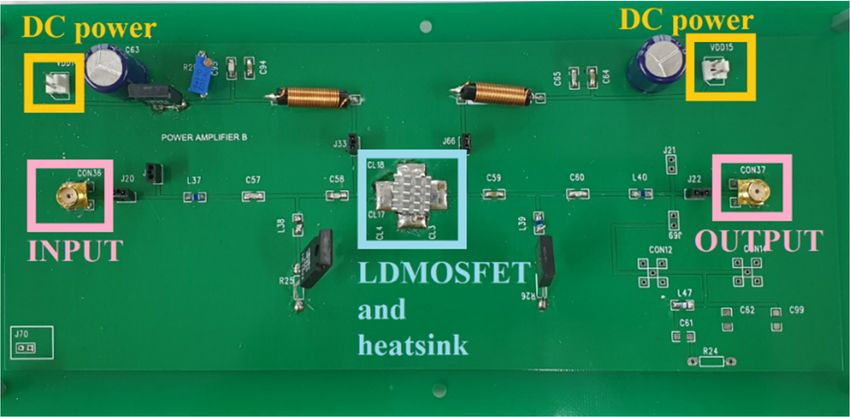
Figure 11a,b shows the manufactured single-ended power amplifier and BWE circuits,
respectively. The main transistor (LDMOSFET) with a heatsink was used to release heat
more effectively [72–74]. The output port in Figure 11b is connected to the input port, as
shown in Figure 11a.nals.
3. Results
Figure 11a,b shows the manufactured single-ended power amplifier and BWE cir-
Sensors 2021, 21, 2356 cuits, respectively. The main transistor (LDMOSFET) with a heatsink was used to release 12 of 18
heat more effectively [72–74]. The output port in Figure 11b is connected to the input port,
as shown in Figure 11a.
(a)
(b)
Figure 11.11.
Figure Manufactured (a) (a)
Manufactured amplifier andand
amplifier (b)(b)
BWE circuits.
BWE circuits.
3.1.3.1.
Performance Comparison
Performance andand
Comparison Analysis of the
Analysis Amplifier
of the Only
Amplifier andand
Only Amplifier + BWE
Amplifier Circuit
+ BWE Circuit
Figure 12a,b shows the POUT and gain variances as the input signal increases. The
black line shows the performance of the power amplifier. The red, blue, and khaki lines
show the performance of the amplifier with the BWE circuit using 0V, 1V, and 3V DC,
respectively. In the case of amp + BWE (0 V) and amp + BWE (1 V), the active device of
the BWE (see M1 in Figure 4) is not in operation, and thus, they have almost the same
performance. Therefore, the red line is almost identical to the blue line. In Figure 12a,b, the
performance of the power amplifier has a higher POUT and gain than the amplifier with a
BWE (3 V) of between −10 dBm and 10 dBm .mately 30%, and the gain bandwidth increases by approximately 56.9%. In this paper, the
BWE circuit is used to widen the bandwidth by lowering the input impedance of the
power amplifier. However, it does not decrease input impedance linearly at all frequen-
cies. As shown in the experimental results, the bandwidth at the high-frequency range is
Sensors 2021, 21, 2356 wider than that of the low-frequency range because the BWE circuit has more impedance
13 of 18
reduction at high frequency (See Figure 12c,d).
Sensors 2021, 21, x FOR PEER REVIEW 14 of 19
(a) (b)
(c) (d)
Figure 12. (a) Pout vs. PIN, (b) gain vs. PIN, (c) Pout vs. frequency, and (d) gain vs. frequency of the performance measurement
Figure 12. (a) Pout vs. PIN , (b) gain vs. PIN , (c) Pout vs. frequency, and (d) gain vs. frequency of the performance
results of the amplifier only and the amplifier with the addition of the BWE circuit.
measurement results of the amplifier only and the amplifier with the addition of the BWE circuit.
Figure12c,d
Figure 13 is the
showsgraph
the of the and
POUT power added
gain efficiency
according (PAE) ofvariations
to frequency the amp and the
at an amp
input
power of −6.5. In Figure 12c,d, the performances of the amplifier at 5–16 MHz havethe
+ BWE (3 V) at 15 MHz. The PAE indicates how much DC power was used to amplify a
input signal
higher [15,75].
POUT and gainInthan
Figure
the13, the PAE
power amplifier PIN of
versuswith BWEthe (3
ampV).(44.8%) is higher than
The performance the
of the
amp +amplifier
power BWE (3 V) (41.2%)
with a BWEwhen
(3 V)10 dBamhigher
has input power
POUT andis applied. This is
gain of 17–35 because
MHz, the addi-
compared to
tional DC power is used for the designed BWE, and the amp has a higher
the power amplifier only. The POUT of the power amplifier with BWE (3V) outperformed P OUT versus the
PIN than
that of thethe amp +amplifier
power BWE (3 V). As16.132
after a result, the PAEs
MHz. of the amp
In addition, the −and thePamp
3 dB + BWE (3V)
OUT bandwidth
do not show a big difference between them.
of the power amplifier only and the power amplifier with BWE (3 V) were 51.5% and
81.5%, respectively. The −3 dB gain bandwidth of the power amplifier only and the power
amplifier with BWE (3 V) are 84.1% and 141%, respectively. By incorporating the BWE
circuit into the power amplifier, the POUT decreases to 0.8 dBm , and the gain decreases
by 0.8 dB when the PIN is −10 dBm . Theoretically, the magnitude of the transfer function
increases with the addition of the BWE circuit to the power amplifier. Although the POUT
and gain should be increased together, in practice, the final output signal can be slightly
reduced because of the power loss of the passive components in the BWE circuit. However,
in the graphs of the POUT and gain versus frequency, the POUT bandwidth increases by
approximately 30%, and the gain bandwidth increases by approximately 56.9%. In this
paper, the BWE circuit is used to widen the bandwidth by lowering the input impedance
of the power amplifier. However, it does not decrease input impedance linearly at all
frequencies. As shown in the experimental results, the bandwidth at the high-frequency
range is wider than that of the low-frequency range because the BWE circuit has more
impedance reduction at high frequency (See Figure 12c,d)
Figure 13 is the graph of the power added efficiency (PAE) of the amp and the amp +
BWE (3 V) at 15 MHz. The PAE indicates how much DC power was used to amplify the
Figure 13. Power added efficiency (PAE) vs. PIN measured results of the amplifier only and the
amplifier with the addition of the BWE circuit.(c) (d)
Figure 12. (a) Pout vs. PIN, (b) gain vs. PIN, (c) Pout vs. frequency, and (d) gain vs. frequency of the performance measurement
results of the amplifier only and the amplifier with the addition of the BWE circuit.
Sensors 2021, 21, 2356 14 of 18
Figure 13 is the graph of the power added efficiency (PAE) of the amp and the amp
+ BWE (3 V) at 15 MHz. The PAE indicates how much DC power was used to amplify the
input signal [15,75]. In Figure 13, the PAE versus PIN of the amp (44.8%) is higher than the
amp input signal
+ BWE [15,75].
(3 V) (41.2%)Inwhen
Figure1013,
dBthe PAEpower
m input versusisPIN of the This
applied. ampis(44.8%)
becauseis the
higher than
addi-
theDC
tional amp + BWE
power (3 V)for
is used (41.2%) when 10BWE,
the designed dBm and
input thepower is applied.
amp has a higherThis
POUTisversus
because
thethe
PIN additional
than the ampDC +power
BWE is(3used forathe
V). As designed
result, BWE,
the PAEs ofand
the the
ampampandhas
theaamp
higher POUT(3V)
+ BWE versus
the P
do not show
IN than the amp + BWE (3 V).
a big difference between them.As a result, the PAEs of the amp and the amp + BWE
(3V) do not show a big difference between them.
Figure 13. Power added efficiency (PAE) vs. PIN measured results of the amplifier only and the
Figure 13. Power added efficiency (PAE) vs. PIN measured results of the amplifier only and the
amplifier with the addition of the BWE circuit.
amplifier with the addition of the BWE circuit.
3.2. Echo Signal Performance Comparison and Analysis
3.2. Echo Signal Performance Comparison and Analysis
Figure 14 shows measured echo signal performances when using 10, 15, 20, and
25Figure 14 shows measured
MHz ultrasound transducers. echo signal
When theperformances when using
ultrasound transducers with 10,
the15, 20, and
same 25
frequency
MHz ultrasound transducers. When the ultrasound transducers with the same
were used, the distance to the target was exactly the same. The input signal was measured frequency
were used,
using the distance
a four-cycle to the
burst target
wave was
with exactly resonant
a suitable the same.frequency
The inputforsignal was measured
the transducer probes.
using
Theameasurement
four-cycle burst wave with
environment of aeach
suitable resonant
frequency is thefrequency
same except for for
thethe
transducer
presence of
probes.
BWEThe with measurement
different DCenvironment
voltages. Asofshown
each frequency
in Figure is 14,the same
the red,except for the
blue, and pres-
khaki lines
ence of BWE
show with differentofDC
the performance thevoltages. As shownonly
power amplifier in Figure 14,power
and the the red, blue, and
amplifier khaki
with BWE
lines showusing
circuit the performance
0 V, 1 V, and 3Vof DC,
the power amplifier
respectively. only
In the caseand theamplifier
of the power amplifier
+ BWE (0with
V) and
BWE circuit using
amplifier + BWE0 (1
V,V),
1 V, and
the 3V DC,(referring
MOSFET respectively.
to M1 Ininthe case of
Figure 4),the amplifier
which + BWEdevice
is the active (0
of the BWE circuit, is not operated and thus shows almost the same performances.
Figure 14a,b shows the measured results of the pulse widths and amplitudes over
the time scale. Figure 14a shows the pulse width according to the frequency. The experi-
mental results showed no significant difference in any of the measured frequency bands.
Experimentally, the BWE circuit does not have a significant influence on the pulse width
of the echo signals. Figure 14b shows the measured echo amplitudes of the peak-to-peak
voltage according to the frequency using a 32 dB preamplifier. As shown in the graph, the
amplitude of amp + BWE (3 V) was higher than that of the amp after 15 MHz. At 25 MHz,
there is a difference of approximately 2.4 dBm . Since the echo signal has an extremely low
amplitude, a 2.4 dBm increment in the amplitude is an attractive result.
Figure 14c,d shows the calculated FFT data used to measure the harmonics and −6 dB
bandwidths of the measured echo signals. Figure 14c shows the THD (%) according to the
frequency. At 20 MHz, the THD of the amp was calculated as 7.15%, which is less than
that of the amp + BWE (3 V). However, at 25 MHz, the THD of the amp was calculated as
15.63%, and that of the amp + BWE (3 V) was calculated as 5.74%. Figure 14d shows the
echo bandwidth according to the frequency. By adding a BWE (3 V) circuit to the power
amplifier, the −6 dB bandwidth of the echo signal was increased by 0.7%, 8.1%, 6.0%, and
9.8% at 10, 15, 20, and 25 MHz, respectively. The bandwidth of the echo signal is actually
related to the axial resolution of the ultrasound image, and thus, a wider bandwidth can
possibly improve the axial resolution [11]. By adding a BWE circuit to the power amplifier,Sensors 2021, 21, 2356 15 of 18
the bandwidth of the echo signal is increased, which can help improve the quality of the
echo signals.amplifier, the −6 dB bandwidth of the echo signal was increased by 0.7%, 8.1%, 6.0%, and
9.8% at 10, 15, 20, and 25 MHz, respectively. The bandwidth of the echo signal is actually
related to the axial resolution of the ultrasound image, and thus, a wider bandwidth can
possibly improve the axial resolution [11]. By adding a BWE circuit to the power amplifier,
Sensors 2021, 21, 2356 the bandwidth of the echo signal is increased, which can help improve the quality16ofof the
18
echo signals.
(a) (b)
(c) (d)
Figure 14. (a) Pulse width vs. frequency, (b) amplitude vs. frequency, (c) total harmonic distortion (THD) vs. frequency, and
(d) bandwidth vs. frequency of the measured echo signal data using 10, 15, 20, and 25 MHz ultrasonic probes.
Both low and high-frequency transducers can be utilized by using the proposed BWE
circuit with the amplifier. There are some ultrasound applications that utilize dual-band
transducer applications [76]. For these applications, the signals of low- and high-frequency
ranges from dual-band therapeutic/imaging transducer applications need to be obtained.
From the paper, the ultrasound transducers enable therapeutic and imaging modes if
needed. A treatment application requires to use many cycle sinusoidal waveforms [77].
The harmonic components generated when amplifying the input signal can affect the signal
quality of the echo signals [78]. For low-frequency therapeutic applications, the harmonic
components can distort the signal and attenuate the depth of penetration [79]. Therefore,
the amplifiers used for therapeutic applications are preferred to have a narrow bandwidth
in order to minimize harmonic components. For high-frequency imaging applications, the
wider bandwidth, the higher axial resolution can be achieved [80]. Therefore, an amplifier
with wide bandwidth is preferred. Hence, our proposed scheme could be useful for such
dual-band transducer applications.
4. Conclusions
The transducers used in ultrasound systems have their own different frequency bands,
depending on the particular purpose and testing area. Therefore, it is necessary to use an
electrical circuit with a wide bandwidth such that the output signal of the transmitter can
cover various ultrasound transducers. One way of expanding the bandwidth is impedance
matching. Impedance matching is required to maximize the amplitudes or bandwidths
of the output signals to the transducer. However, an impedance-matching job that canSensors 2021, 21, 2356 17 of 18
cover such wide transducers is extremely difficult because the impedance is different for
each transducer. Although impedance matching is not taken into account in this document,
it is clear that impedance matching can be used if we know the impedance values of the
predetermined transducer. However, this method used to increase the bandwidth could
possibly lower the output amplitude at the center frequency. In addition, the feedback loop
circuit methodology can increase the bandwidth by reducing the output amplitude of the
power amplifier. Therefore, we propose a switching mode transmit circuit that can widen
the bandwidth and minimize the output amplitude as needed. The designed BWE circuit
changes the performance of the power amplifier because the bandwidth in the transfer
function is widened by moving the input pole of the power amplifier.
To verify our proposed concept and verify the performance results, we tested a
power amplifier equipped with a BWE circuit under the same conditions. Comparing the
performances of the manufactured amplifier only and the amplifier with the BWE circuit,
the POUT and gain values of the amplifier with the BWE circuit were decreased slightly to
0.8 dBm and 0.8 dB; however, the POUT bandwidth increased by approximately 30%, and
the gain bandwidth increased by approximately 56.9% at −6.5 dBm of input power. In
addition, the echo bandwidths were expanded by 0.7%, 8.1%, 6.0%, and 9.8% at frequencies
of 10, 15, 20, and 25 MHz, respectively.
In practice, the measured experimental data may be different from the theoretical
data because there are various side effects caused by signal distortions of different fre-
quency characteristics and parasitic components of the elements. From the experimental
results, none of the measured performances were enhanced when adding a functional
BWE circuit. Although the bandwidth is wider, there is a slight compromise, such as a
decline in output power or an increase in THD (%). However, the manufactured BWE
circuit improves the bandwidth and minimizes the amplitude of the power amplifier to
support higher operating transducer probes, thus possibly helping improve the ultrasound
system resolution.
Author Contributions: Conceptualization, K.K. and H.C.; methodology, K.K. and H.C.; formal
analysis, K.K.; writing—original draft preparation, K.K. and H.C. All authors have read and agreed
to the published version of the manuscript.
Funding: This work was supported by a National Research Foundation of Korea grant funded by
the government (MSIT) (No. 2020R1A2C4001606). This work was supported by project for Industry-
Academic Cooperation Based Platform R&D funded Korea Ministry of SMEs and Startups in 2020
(Project No. S3010583).
Institutional Review Board Statement: Not applicable.
Informed Consent Statement: Not applicable.
Data Availability Statement: The data presented in this study are available on request from the
corresponding author.
Conflicts of Interest: The authors declare no conflict of interest.
References
1. Shung, K.K. Diagnostic Ultrasound: Imaging and Blood Flow Measurements; Taylor & Francis: Boca Raton, FL, USA, 2015.
2. Szabo, T.L. Diagnostic Ultrasound Imaging: Inside Out; Elsevier Academic Press: London, UK, 2013.
3. Zhou, Q.; Lau, S.; Wu, D.; Shung, K.K. Piezoelectric films for high frequency ultrasonic transducers in biomedical applications.
Prog. Mater. Sci. 2011, 56, 139–174. [CrossRef] [PubMed]
4. Zhu, B.; Fei, C.; Wang, C.; Zhu, Y.; Yang, X.; Zheng, H.; Zhou, Q.; Shung, K.K. Self-focused AlScN film ultrasound transducer for
individual cell manipulation. ACS Sens. 2017, 2, 172–177. [CrossRef] [PubMed]
5. Hoskins, P.R.; Martin, K.; Thrush, A. Diagnostic Ultrasound: Physics and Equipment; Cambridge University Press: Cambridge, UK, 2019.
6. Postema, M. Fundamentals of Medical Ultrasound; Taylor and Francis: New York, NY, USA, 2011.
7. Kremkau, F.W.; Forsberg, F. Sonography Principles and Instruments; Elsevier Health Sciences: Amsterdam, The Netherlands, 2015.
8. Li, X.; Wei, W.; Zhou, Q.; Shung, K.K.; Chen, Z. Intravascular photoacoustic imaging at 35 and 80 MHz. J. Biomed. Opt. 2012,
17, 106005. [CrossRef]You can also read