One transistor static random access memory cell array comprising single gated feedback field effect transistors
←
→
Page content transcription
If your browser does not render page correctly, please read the page content below
www.nature.com/scientificreports
OPEN One‑transistor static
random‑access memory cell array
comprising single‑gated feedback
field‑effect transistors
Sangik Choi1, Jaemin Son2, Kyoungah Cho2 & Sangsig Kim1,2*
In this study, we fabricated a 2 × 2 one-transistor static random-access memory (1T-SRAM) cell array
comprising single-gated feedback field-effect transistors and examined their operation and memory
characteristics. The individual 1T-SRAM cell had a retention time of over 900 s, nondestructive reading
characteristics of 10,000 s, and an endurance of 108 cycles. The standby power of the individual
1T-SRAM cell was estimated to be 0.7 pW for holding the “0” state and 6 nW for holding the “1”
state. For a selected cell in the 2 × 2 1T-SRAM cell array, nondestructive reading of the memory was
conducted without any disturbance in the half-selected cells. This immunity to disturbances validated
the reliability of the 1T-SRAM cell array.
Over the years, various studies have been conducted to overcome the issues posed by the size and power con-
sumption of conventional static random-access memory (SRAM)1–4. Decreasing the number of component
transistors in conventional SRAM cells has been suggested as a suitable way to combat these problems5–13.
However, reduction in the operation power of SRAM cells remains a challenging issue. This is mainly because
the low-power operation of SRAM cell arrays decreases the reliability of memory operation due to disturbances
caused by the half selected c ell14–16.
More recently, simulation studies have demonstrated that the low standby power consumption and reliability
of one-transistor SRAM (1T-SRAM) cells, each of which consists of a single-gated feedback field-effect transistor
(FBFET), provide a promising possibility for the future of memory devices17. Compared with metal–oxide–semi-
conductor field-effect transistors (MOSFETs) conventionally used in SRAM cells, FBFETs, operating with a posi-
tive feedback loop mechanism, exhibit an extremely low subthreshold swing (~ 0 mV/dec), high on/off current
ratios, and bi-stable states18–22. Moreover, the use of 1T-SRAM cells reduces usage area on chips when compared
with conventional 6T-SRAM cells constructed with MOSFETs. Hence, FBFETs are more advantageous than
MOSFETs in terms of usage in SRAM cells, thus increasing performance while reducing their size. To apply our
1T-SRAM cell to computing systems, the reliability of the cell array should be confirmed. Hence, in this study,
we fabricated a 2 × 2 1T-SRAM cell array using four FBFETs and confirmed its immunity against half-selected
cell disturbances during nondestructive reading of the memory.
Experimental section
Figure 1 shows the schematic of a 2 × 2 1T-SRAM cell array consisting of four p-channel FBFETs with a p+-n-p-n+
structure and with each channel (gated or non-gated) being 1.5 μm in length. Herein, four p-channel FBFETs
stand for four SRAM cells because only one transistor performs the function of a SRAM cell in our device
structure. The 1T-SRAM cells were fabricated on an SOI wafer with 2-μm-thick buried oxide through a CMOS-
compatible process. First, a 340 nm silicon active layer was prepared using stepper photolithography and an
anisotropic dry etching process. The n-well was formed by the implantation of P + ions at a dose of 3 × 1013 cm−2
with an ion energy of 60 keV, annealed at 1100 °C for 30 min. The p-type channel region was formed by the
implantation of B F2+ ions at a dose of 6 × 1013 cm−2 with an ion energy of 40 keV. For the formation of the n+
source and p+ drain regions, P+ and B F2+ ions were implanted at a dose of 3 × 1015 cm−2 using a masked ion
implantation method at ion energies of 100 keV and 30 keV, respectively. A 22-nm-thick SiO2 gate dielectric
was thermally grown at 850 °C for 300 min, before a 400-nm-thick poly-Si gate was formed using low-pressure
1
Department of Semiconductor Systems Engineering, Korea University, 145 Anam‑ro, Seongbuk‑gu, Seoul 02841,
Republic of Korea. 2Department of Electrical Engineering, Korea University, 145 Anam‑ro, Seongbuk‑gu,
Seoul 02841, Republic of Korea. *email: sangsig@korea.ac.kr
Scientific Reports | (2021) 11:17983 | https://doi.org/10.1038/s41598-021-97479-x 1
Vol.:(0123456789)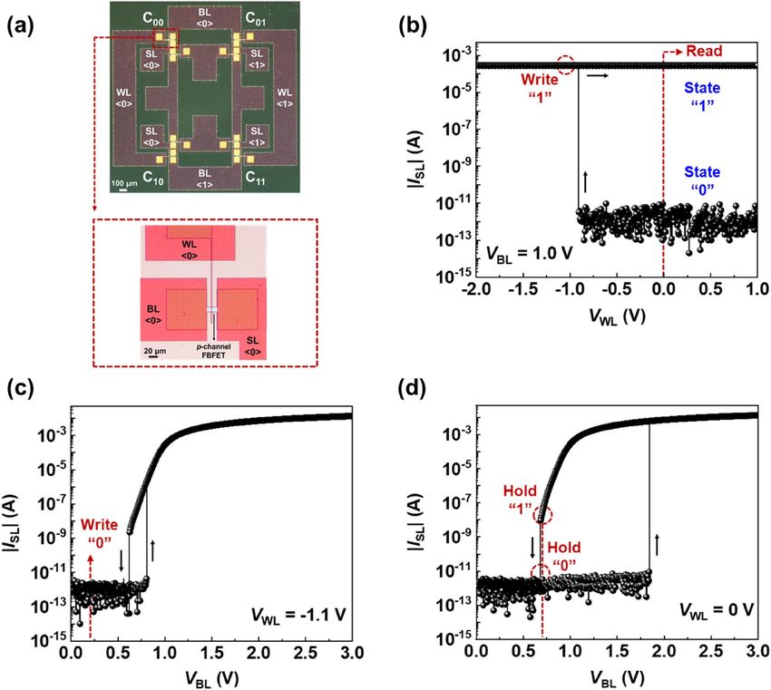
www.nature.com/scientificreports/
Figure 1. Schematics of a 2 × 2 array of 1T-SRAM cells and a p-channel FBFET.
chemical vapor deposition, photolithography, and a dry etching process. Finally, a Ti/TiN/Al/TiN metal alloy
was deposited for the bit line (BL), word line (WL), and source line (SL) contacts. The 2 × 2 1T-SRAM cell array
was completed with shared BLs horizontally and shared WLs and SLs vertically.
The electrical characteristics were measured at room temperature using a semiconductor parameter analyzer
(HP4155C, Agilent), a Tektronix AFG 31,000 arbitrary function generator, a Tektronix MDO3054 mixed-domain
oscilloscope, and a Keithley 2636 B sourcemeter SMU instrument. The limits of the retention and endurance
measurement were 900 s and 1 08 cycles, respectively.
Results and discussion
The optical images in Fig. 2a show our 2 × 2 1T-SRAM cell array consisting of four cells (i.e., C 00, C01, C10, and
C11), where C00 shares BL and WL with C01 and C10, while C11 shares WL and BL with C01 and
C10. The transfer function in Fig. 2b shows the bistable states for an individual 1T-SRAM cell. The abrupt increase
in |ISL| when VWL reached − 0.91 V in the transfer function indicates the latch-up phenomenon, which induces
a positive feedback loop. Herein, negative VWL and positive VBL are responsible for barrier-height modulation.
Carrier accumulation in the potential wells of the conduction and valence bands in the channels of the FBFET
determine the current state. Our 1T-SRAM cell uses holes as the majority charge carriers for the positive feedback
loop. The “0” and “1” states are described by the absence and presence of excess charge carriers in the potential
Scientific Reports | (2021) 11:17983 | https://doi.org/10.1038/s41598-021-97479-x 2
Vol:.(1234567890)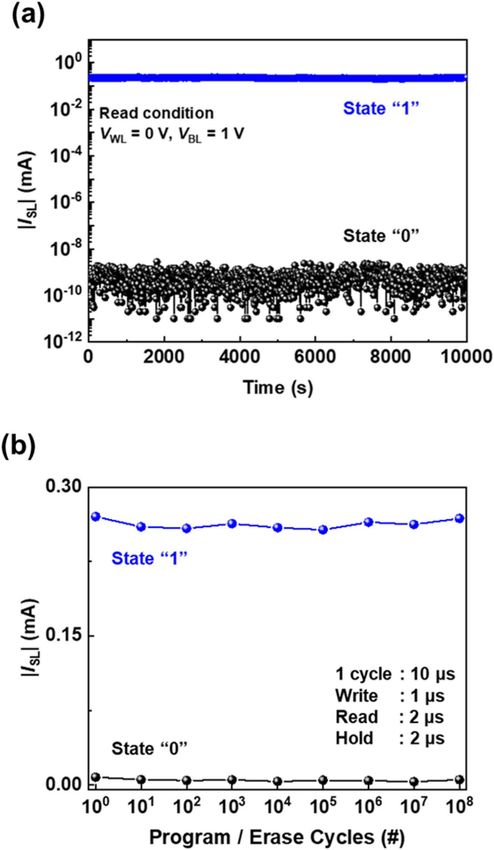
www.nature.com/scientificreports/
Figure 2. (a) Optical image of a 2 × 2 1T-SRAM cell array and a p-channel FBFET. (b) Transfer function
of a selected 1T-SRAM cell at VBL = 1.0 V. Output curves of the 1T-SRAM cell at (c) VWL = − 1.1 V and (d)
VWL = 0.0 V.
wells, respectively. For the write “1” (W1) operation, VWL was selected to be − 1.1 V, which is below the latch-up
voltage of − 0.91 V. The read “1” and “0” (R1, R0) operations were carried out at VWL = 0.0 V, and R0 and R1 states
are triggered before and after the W1 operation. The hysteresis characteristics of the output functions for each
individual 1T-SRAM cell are shown in Fig. 2c,d. These curves are used to determine the remaining operations.
VBL was increased in a forward sweep from 0 to 3 V, |ISL| abruptly increased at two points, at a VBL of 0.81 V
for VWL = − 1.1 V and at a VBL of 1.85 V for VWL = 0 V. However, during the reverse sweep, |ISL| fell abruptly at a
VBL of 0.68 V, which indicates the latch-down phenomenon. For the operations of the 1T-SRAM cell, VBL was
selected to be 0.2 V for the write “0” (W0) operation and 0.68 V for the hold “1” and “0” (H1, H0) operations.
A timing diagram for a sequence of the write, hold, and read operations of the 1T-SRAM cell is shown in
Fig. 3. Here, the W1, W0, H1, and H0 operations were performed for 200 ns, and the R1 and R0 operations
were performed for 400 ns. The operating conditions are presented in Table 1. A delay time of 140 ns in |ISL|
was inherent in the measurement system; nevertheless, our 1T-SRAM cell worked without any malfunction.
The cycle starts after the H1 operation, and during the R1 operation, |ISL| was 300 μA, indicating the “1” state.
Next, the W0 operation was performed at a VBL of 0.2 V and at a VWL of − 1.1 V, at which point |ISL| became ~ 1
pA. The decreases in VBL and negative VWL are responsible for breaking the positive feedback loop. After the H0
operation, the R0 operation |ISL| was kept at ~ 1 pA, indicating the “0” state. Although VBL and VWL are the same
for the R0 and R1 operations, there is a differing |ISL| value, which is determined by the previous W0 or W1
|ISL| values, respectively. |ISL| was ~ 1 pA for the H0 operation and ~ 9 nA for the H1 operation. The magnitude
of |ISL| was used to calculate the standby power consumption. The standby power consumption was 0.7 pW for
the “0” state and 6 nW for the “1” state. In this regard, the standby power consumption of our 1T-SRAM cell is
superior to other SRAM cells23–26.
Figures 4 show the retention characteristics of the “1” (a) and “0” (b) states after a holding time of 900 s.
During the H1 operation, there was no loss in charge carriers accumulated in the channel; consequently, |ISL| in
the R1 operation was 300 μA, which is the same as that of the W1 operation. On the other hand, the absence of
Scientific Reports | (2021) 11:17983 | https://doi.org/10.1038/s41598-021-97479-x 3
Vol.:(0123456789)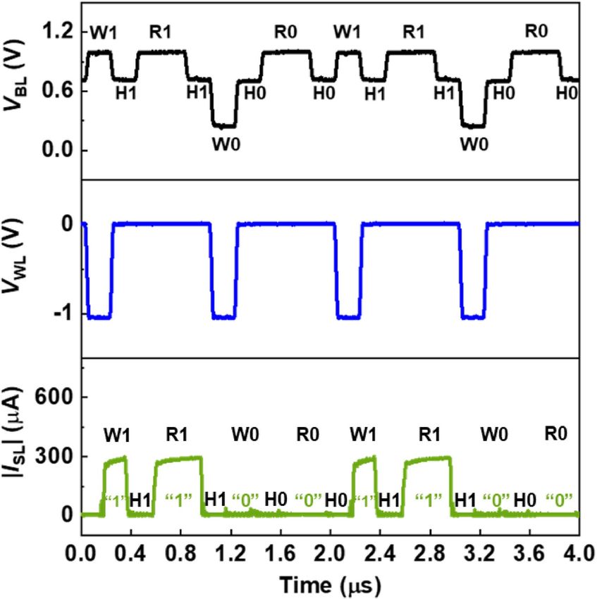
www.nature.com/scientificreports/
Figure 3. Timing diagrams of 1T-SRAM cell memory operations. The pulse width of the write and hold
operations was 200 ns, and the pulse width of the read operation was 400 ns.
Voltage Write “1” Write “0” Read Hold
VBL (V) 1.0 0.2 1.0 0.68
VWL (V) − 1.1 − 1.1 0.0 0.0
Table 1. Operating conditions of the 1T-SRAM cell.
charge carriers in the potential well during the W0 operation produced |ISL| of 1 pA during the H0 operation. This
|ISL| became the output signal for the R0 operation. The detection limit during experimentation was 900 s; this
was mainly due to the test equipment constraints and the memory retention of the 1T-SRAM cell is much longer.
The nondestructive reading characteristics of the 1T-SRAM cell shown in Fig. 5a reveals that the “1” and
“0” states were maintained for 10,000 s, with a sensing margin of 109, when |ISL| was under the read conditions
of VWL = 0 V and VBL = 1 V. These excellent nondestructive reading characteristics show that the states are not
destroyed during the reading operation even over an extended period and there is no degradation associated
with the accumulation of charge carriers in the channel region. The endurance of the 1T-SRAM cell shown in
Fig. 5b indicates the maintenance of the “0” and “1” states even after 1 08 cycles where one cycle consists of the
program and erase operations. The |ISL| magnitude in the “0” state is a few μA being the detection limit of our
measurement system so that the sensing margin for the endurance becomes 1 02. Considering these criteria, our
1T-SRAM cell can be considered a reliable memory device.
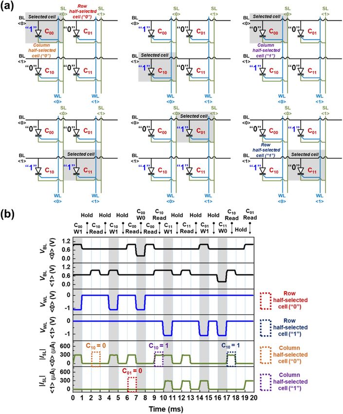
To further examine the reliability of the 2 × 2 1T-SRAM cell array, memory operations were performed to
monitor the half-selected cells, as shown in Fig. 6. For example, when C00 was selected, C01 and C10 became
the row and column half-selected cells respectively, as shown in Fig. 6a. The operations of the row and column
Scientific Reports | (2021) 11:17983 | https://doi.org/10.1038/s41598-021-97479-x 4
Vol:.(1234567890)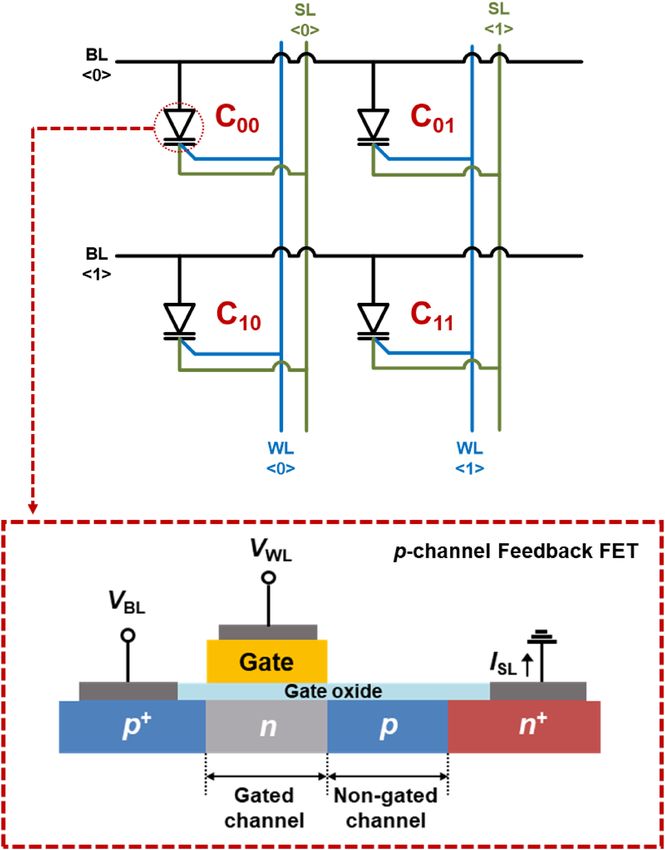
www.nature.com/scientificreports/
Figure 4. Retention characteristics of (a) the “1” state and (b) the “0” state.
half-selected cells are influenced by BL and WL disturbances, respectively. Figure 6b shows the timing diagrams
of the array. The W1 operation at C 00 was carried out at a VBL of 1.0 V, VWL of − 1.1 V, and an |ISL| of 300
μA which produces the “1” state output. When the read operation at C 10, which shares WL with C 00, was
performed after the hold operation, |ISL| indicates the output signal was in the “0” state. This demonstrates that
there was no disturbance in the column half-selected cell. For the read operation at C01, which shares BL with
C00, |ISL| indicates the output signal was in the “0” state, implying immunity against disturbance in the half-
selected cell rows. Thus, there was no disturbance in half-selected cells for both the rows and columns when C 00
was in the “1” state. In addition, the states of the column and row half-selected cells for C00 in the “0” state were
unchanged even after the W1 operation at C00. Moreover, the immunity against disturbance in the half-selected
cells in the “0” state was reaffirmed by the read operation at C10 after the W0 operation at C11 while having a
shared BL line. Our 1T-SRAM cell array demonstrates reliability in nondestructive readout operations.
Considering that only one transistor performs the function of a SRAM cell, our SRAM cells have advantages of
lower power operation and reduced size, compared to conventional SRAM cells.
Scientific Reports | (2021) 11:17983 | https://doi.org/10.1038/s41598-021-97479-x 5
Vol.:(0123456789)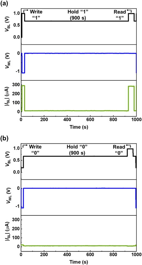
www.nature.com/scientificreports/
Figure 5. For 1T-SRAM cell: (a) nondestructive reading characteristics at VWL = 0.0 V and VBL = 1.0 V and (b)
endurance characteristics.
Conclusions
In this study, we fabricated a 2 × 2 1T-SRAM cell array and investigated its operation and memory characteristics.
An individual 1T-SRAM cell consumed 0.7 pW for holding the “0” state and 6 nW for holding the “1” state. The
cells had a retention time of over 900 s, nondestructive reading characteristics of 10,000 s, and an endurance of
108 cycles. Furthermore, nondestructive memory reading operations were conducted without any disturbance
to the half-selected cells validating the reliability of the array. The size and power consumption of our 1T-SRAM
cell array means that it can be used for computing systems that require a large amount of on-chip memory.
Scientific Reports | (2021) 11:17983 | https://doi.org/10.1038/s41598-021-97479-x 6
Vol:.(1234567890)www.nature.com/scientificreports/
Figure 6. For 2 × 2 1T-SRAM cell array: (a) schematic diagram of the memory operations and (b) timing
diagrams.
Received: 11 June 2021; Accepted: 19 August 2021
References
1. Song, T. et al. A 10 nm FinFET 128 Mb SRAM with assist adjustment system for power, performance, and area optimization. IEEE
J. Solid-State Circuits 52(1), 240–249 (2016).
2. Deepak, N. & Kumar, R. B. Certain investigations in achieving low power dissipation for SRAM cell. Microprocessors Microsyst.
77, 103166 (2020).
Scientific Reports | (2021) 11:17983 | https://doi.org/10.1038/s41598-021-97479-x 7
Vol.:(0123456789)www.nature.com/scientificreports/
3. Chang, L. et al. Stable SRAM cell design for the 32 nm node and beyond. In Digest of Technical Papers. 2005 Symposium on VLSI
Technology, 128–129. https://doi.org/10.1109/.2005.1469239 (2005).
4. Gupta, S., Gupta, K., Calhoun, B. H. & Pandey, N. Low-power near-threshold 10T SRAM bit cells with enhanced data-independent
read port leakage for array augmentation in 32-nm CMOS. IEEE Trans. Circuits Syst. I. Regular Papers 66(3), 978–988 (2018).
5. Gupta R., Gill S. S., & Kaur, N. A novel low leakage and high density 5T CMOS SRAM Cell in 45nm technology. In 2014 Recent
Advances in Engineering and Computational Sciences (RAECS), 1–6. https://doi.org/10.1109/RAECS.2014.6799650 (2014).
6. Akashe, S. & Sharma, S. High density and low leakage current based SRAM cell using 45 nm technology. Int. J. Electron. 100(4),
536–552 (2013).
7. Mishra, J. K., Misra, P. K. & Goswami, M. A low power 7T SRAM cell using supply feedback technique at 28nm CMOS technol-
ogy. In 2020 7th International Conference on Signal Processing and Integrated Networks (SPIN), 597–602. https://doi.org/10.1109/
SPIN48934.2020.9071308 (2020).
8. Pasandi, G. & Fakhraie, S. M. An 8T low-voltage and low-leakage half-selection disturb-free SRAM using bulk-CMOS and FinFETs.
IEEE Trans. Electron Devices 61(7), 2357–2363 (2014).
9. Jung, S. O. et al. Power-gated 9T SRAM cell for low-energy operation. IEEE Trans. Very Large Scale Integr. Syst. 25(3), 1183–1187
(2016).
10. Singh, A. K., Seong, M. M. & Prabhu, C. M. R. A data aware 9T static random access memory cell for low power consumption and
improved stability. Int. J. Circuit Theory Appl. 42(9), 956–966 (2014).
11. Lo, C. H. & Huang, S. Y. PPN based 10T SRAM cell for low-leakage and resilient subthreshold operation. IEEE J. Solid-State Circuits
46(3), 695–704 (2011).
12. Han, J. W. et al. A novel bi-stable 1-transistor SRAM for high density embedded applications. In 2015 IEEE International Electron
Devices Meeting (IEDM), 26.27.21–26.27.24. https://doi.org/10.1109/IEDM.2015.7409776 (2015).
13. Widjaja, Y. et al. A bi-stable 1-/2-transistor SRAM in 14 nm FinFET technology for high density/high performance embedded
applications. In 2018 IEEE International Electron Devices Meeting (IEDM), 18.16.11–18.16 .14. https://doi.org/10.1109/IEDM.
2018.8614555 (2018).
14. Ensan, S. S., Moaiyeri, M. H., Moghaddam, M. & Hessabi, S. A low-power single-ended SRAM in FinFET technology. AEU-Int.
J. Electron Commun. 99, 361–368 (2019).
15. Ahmad, S., Alam, N. & Hasan, M. Pseudo differential multi-cell upset immune robust SRAM cell for ultra-low power applications.
AEU-Int. J. Electron Commun. 83, 366–375 (2018).
16. Pal, S., Gupta, V., Ki, W. H. & Islam, A. Transmission gate-based 9T SRAM cell for variation resilient low power and reliable internet
of things applications. IET Circuits Devices Syst. 13(5), 584–595 (2019).
17. Cho, J., Lim, D., Woo, S., Cho, K. & Kim, S. Static random access memory characteristics of single-gated feedback field-effect
transistors. IEEE Trans. Electron Devices 66(1), 413–419 (2018).
18. Padilla A., Yeung, C. W., Shin, C., Hu, C. & Liu, T. J. K. Feedback FET: a novel transistor exhibiting steep switching behavior at
low bias voltages. In 2008 IEEE International Electron Devices Meeting, 1–4. https://doi.org/10.1109/IEDM.2008.4796643 (2008).
19. Wan, J., Cristoloveanu, S., Le Royer, C. & Zaslavsky, A. A feedback silicon-on-insulator steep switching device with gate-controlled
carrier injection. Solid-State Electron. 76, 109–111 (2012).
20. Kim, H., Hwang S., Kwon, D. W., Lee, J. H. & Park, B. G. Back biasing effects in a feedback steep switching device with charge
spacer. In 2016 IEEE Silicon Nanoelectronics Workshop (SNW), 172–173. https://doi.org/10.1109/SNW.2016.7578037 (2016).
21. Jeon, Y., Kim, M., Lim, D. & Kim, S. Steep subthreshold swing n-and p-channel operation of bendable feedback field-effect transis-
tors with p+–i–n+ nanowires by dual-top-gate voltage modulation. Nano Lett. 15(8), 4905–4913 (2015).
22. Kim, M. et al. Steep switching characteristics of single-gated feedback field-effect transistors. Nanotechnology 28(5), 055205 (2016).
23. Ahmad, S., Gupta, M. K., Alam, N. & Hasan, M. Low leakage single bitline 9 t (sb9t) static random access memory. Microelectron.
J. 62, 1–11 (2017).
24. Ahmad, S., Alam, N. & Hasan, M. Robust TFET SRAM cell for ultra-low power IoT applications. AEU-Int. J. Electron C. 89, 70–76
(2018).
25. Lin, Z. et al. Half-select disturb-free 10T tunnel FET SRAM Cell with improved noise margin and low power consumption. IEEE
Trans. Circuits Syst. II Express Briefs https://doi.org/10.1109/TCSII.2021.3057678 (2021).
26. Wen, L., Li, Z. & Li, Y. Single-ended, robust 8T SRAM cell for low-voltage operation. Microelectron. J. 44(8), 718–728 (2013).
Acknowledgements
This research was partially supported by the Ministry of Trade, Industry & Energy (MOTIE; 10067791) and the
Korea Semiconductor Research Consortium (KSRC) support program for the development of future semicon-
ductor devices. It was also supported by a National Research Foundation of Korea (NRF) grant funded by the
Korean government (MSIT; 2020R1A2C3004538), the Brain Korea 21 Plus Project of 2021 through the NRF
funded by the Ministry of Science, ICT & Future Planning, and the Korea University Grant.
Author contributions
S.C., J.S. and S.K. provided conceptualization and methodology. S.C. and J.S. verified and investigated. S.C., J.S.,
K.C. and S.K. analyzed the results and wrote the manuscript; S.K. supervised the research. All authors edited the
manuscript and have given approval to the final version of the manuscript.
Competing interests
The authors declare no competing interests.
Additional information
Correspondence and requests for materials should be addressed to S.K.
Reprints and permissions information is available at www.nature.com/reprints.
Publisher’s note Springer Nature remains neutral with regard to jurisdictional claims in published maps and
institutional affiliations.
Scientific Reports | (2021) 11:17983 | https://doi.org/10.1038/s41598-021-97479-x 8
Vol:.(1234567890)www.nature.com/scientificreports/
Open Access This article is licensed under a Creative Commons Attribution 4.0 International
License, which permits use, sharing, adaptation, distribution and reproduction in any medium or
format, as long as you give appropriate credit to the original author(s) and the source, provide a link to the
Creative Commons licence, and indicate if changes were made. The images or other third party material in this
article are included in the article’s Creative Commons licence, unless indicated otherwise in a credit line to the
material. If material is not included in the article’s Creative Commons licence and your intended use is not
permitted by statutory regulation or exceeds the permitted use, you will need to obtain permission directly from
the copyright holder. To view a copy of this licence, visit http://creativecommons.org/licenses/by/4.0/.
© The Author(s) 2021
Scientific Reports | (2021) 11:17983 | https://doi.org/10.1038/s41598-021-97479-x 9
Vol.:(0123456789)You can also read