Optimized Memory Allocation and Power Minimization for FPGA-Based Image Processing - MDPI
←
→
Page content transcription
If your browser does not render page correctly, please read the page content below
Journal of
           Imaging
Article
Optimized Memory Allocation and Power
Minimization for FPGA-Based Image Processing
Paulo Garcia 1, * , Deepayan Bhowmik 2 , Robert Stewart 3 , Greg Michaelson 3 and
Andrew Wallace 4
 1   Department of Systems and Computer Engineering, Carleton University, Ottawa, ON K1S 5B6, Canada
 2   Div. of Computing Science and Mathematics, University of Stirling, Stirling FK9 4LA, UK;
     deepayan.bhowmik@stir.ac.uk
 3   School of Mathematical and Computer Sciences, Heriot Watt University, Edinburgh EH14 4AS, UK;
     rstewart@hw.ac.uk (R.S.); gmichaelson@hw.ac.uk (G.M.)
 4   School of Engineering and Physical Sciences, Heriot Watt University, Edinburgh EH14 4AS, UK;
     a.m.wallace@hw.ac.uk
 *   Correspondence: paulogarcia@cunet.carleton.ca

 Received: 19 November 2018; Accepted: 27 December 2018; Published: 1 January 2019

 Abstract: Memory is the biggest limiting factor to the widespread use of FPGAs for high-level
 image processing, which require complete frame(s) to be stored in situ. Since FPGAs have limited
 on-chip memory capabilities, efficient use of such resources is essential to meet performance, size and
 power constraints. In this paper, we investigate allocation of on-chip memory resources in order to
 minimize resource usage and power consumption, contributing to the realization of power-efficient
 high-level image processing fully contained on FPGAs. We propose methods for generating memory
 architectures, from both Hardware Description Languages and High Level Synthesis designs, which
 minimize memory usage and power consumption. Based on a formalization of on-chip memory
 configuration options and a power model, we demonstrate how our partitioning algorithms can
 outperform traditional strategies. Compared to commercial FPGA synthesis and High Level Synthesis
 tools, our results show that the proposed algorithms can result in up to 60% higher utilization
 efficiency, increasing the sizes and/or number of frames that can be accommodated, and reduce
 frame buffers’ dynamic power consumption by up to approximately 70%. In our experiments
 using Optical Flow and MeanShift Tracking, representative high-level algorithms, data show that
 partitioning algorithms can reduce total power by up to 25% and 30%, respectively, without impacting
 performance.

 Keywords: field programmable gate array (FPGA); memory; power; image processing; design

1. Introduction
     Advances in Field Programmable Gate Array (FPGA) technology [1] have made them the de facto
implementation platform for a variety of computer vision applications [2]. Several algorithms, e.g.,
stereo-matching [3], are not feasibly processed in real-time on conventional general purpose processors
and are best suited to hardware implementation [4,5]. The absence of a sufficiently comprehensive,
one size fits all hardware pipeline for the computer vision domain [6] motivates the use of FPGAs
in a myriad of computer vision scenarios, especially in applications where processing should be
performed in situ, such as in smart cameras [7], where FPGAs embed data acquisition, processing and
communication subsystems. Adoption of FPGA technology by the computer vision community has
accelerated during recent years thanks to the availability of High Level Synthesis (HLS) tools which
enable FPGA design within established software design contexts.

J. Imaging 2019, 5, 7; doi:10.3390/jimaging5010007                         www.mdpi.com/journal/jimaging
J. Imaging 2019, 5, 7                                                                             2 of 23

      However, since FPGAs have limited on-chip memory capabilities (e.g., approx. 6MB of on-chip
memory on high end Virtex 7 FPGAs), external memory (i.e., DDR-RAM chips connected to the FPGA)
is often used to accommodate frames [8,9]. This causes penalties on performance (latency is much higher
for off-chip memory access) and perhaps more importantly, on size (two chips, FPGA and DDR, rather
than just FPGA), power (DDR memories are power hungry [10]) and have associated monetary costs,
hindering the adoption of FPGAs.
      In this paper, we research allocation of on-chip memory resources in order to minimize resource
usage and power consumption, contributing to the realization of power-efficient high-level image
processing systems fully contained on FPGAs. We propose methods for generating on-chip memory
architectures, applicable from both HLS and Hardware Description Languages (HDL) designs, which
minimize FPGA memory resource usage and power consumption for image processing applications.
Our approach does not exclude external memory access: rather, it is orthogonal to any memory
hierarchy, and applicable to any instances of on-chip memory. Specifically, this paper offers the
following contributions:
•     A formal analysis of on-chip memory allocation schemes and associated memory usage for given
      frame sizes and possible on-chip memory configurations.
•     Methods for selecting a memory configuration for optimized on-chip memory resource usage and
      balanced usage/power for a given frame size.
•     A theoretical analysis of the effects on resource usage and power consumption of our partitioning
      methods.
•     Empirical validation of resource usage, power and performance of the proposed methods,
      compared to a commercial HLS tool.
     Our experiments show that on-chip memory dynamic power consumption can be reduced by up
to approximately 70%; using representative high-level algorithms, this corresponds to a reduction of
total power by up to 25% and 30%, respectively, without impacting performance. The remainder of
this paper is organized as follows: Section 2 describes related work within FPGA memory systems
architecture and design for image processing. In Section 3, we formally describe the research problem
of power-size optimization, present a motivational example that highlights the limitations of standard
HLS approaches, and present alternative partitioning methods. Section 4 describes our experimental
methodology and experimental results, and Section 5 presents a thorough discussion of said results.
Finally, Section 6 presents our concluding remarks.
     Throughout this paper, we use the term BRAM (Block Random Access Memory), a Xilinx
nomenclature for on-chip memories, to refer to on-chip FPGA memories in general.

2. Background and Related Work
      Within FPGA processing sub-systems, algorithms evolve from typical software-suitable
representations into more hardware-friendly ones [6,11] which can fully exploit data parallelism [11]
through application-specific hardware architectures [3], often substantially different from the
traditional Von Neumann model, such as dataflow [12,13] or biologically inspired processing [14].
These heterogeneous architectures are customized for FPGA implementation not just for performance
(e.g., by exploiting binary logarithmic arithmetic for efficient multiplication/division [15]), but also
for power efficiency (e.g., by static/dynamic frequency scaling across parallel datapaths for reduced
power consumption [16]).
      More often than not, computer vision applications deployed on FPGAs are constrained
by performance, power and real-time requirements [3]. Real time streaming applications (i.e.,
performing image processing on real-time video feeds [6]) require bounded acquisition, processing and
communication times [16] which can only be achieved, while maintaining the required computational
power, through exploitation of data parallelism [11] by dedicated functional blocks [7].
      However, the greatest limiting factor to the widespread use of FPGAs for complex image
processing applications is memory [9]. Algorithms that perform only point or local region operators
J. Imaging 2019, 5, 7                                                                                3 of 23

(e.g., sliding window filters) [15] are relatively simple to implement using hardware structures such as
line buffers [3]. However, complex algorithms based on global operations require complete frame(s) to
be stored in situ [11]; examples of contemporary applications that require global operations are object
detection, identification and tracking, critical to security. Notice we use the term “global operations” to
simultaneously refer to two characteristics: the use of global operators (atomic operations which require
the whole image, such as transposition or rotation) and undetermined (unpredictable) access patterns
(e.g., a person identification system might only need a subset of a frame, but which subset cannot be
decided at design time, as it depends on person location at runtime).
      A possible approach is to refine image processing algorithms so they can perform on smaller frame
sizes that can be contained on an FPGA [2]. Several algorithms maintain robustness for downscaled
images [17], e.g., the Face Certainty Map [18]) or employ intelligent on-chip memory allocation
schemes [8] to accommodate complete frames that take into account power profiles. The latter requires
methods to optimize on-chip memory configurations in order to maximize valuable usage; often at
odds with performance-oriented allocation schemes standard in HLS code generators. Other possible
approaches include stream-processing algorithm refactoring to minimize memory requirements [19]
or programming-language abstractions for efficient hardware pipeline generation [20]; these are
orthogonal to our approach, and outside the scope of this work.
      In our context, the most significant related work on the use of FPGA on-chip memory for image
processing applications has focused on four aspects: processing-specific memory architectures, caching
systems for off-chip memory access, partitioning algorithms for performance and on chip memory
power reduction.

2.1. Processing-Specific Memory Architectures
      Memory architectures specialized for specific processing pipelines typically exhibit poor BRAM
utilization. Torres-Huitzil and Nuno-Maganda [9] presented a mirrored memory system: in order to
cope with dual access required by computational datapaths; data is replicated in two parallel memories
and a third one is used for intermediate computations. The need for data replication to support
paralellism inhibits scaling for higher frame sizes. Mori et al. [21] described the use of neighbourhood
loader: input pixels are fed to shift registers which de-serialize the input stream into a neighbourhood
region. Their approach supports only one output port, and sequential region read (no random access).
This approach does not exploit datapath parallelism, nor does it support classes of algorithms which
require disparate region access. Chen et al. [22] use distributed data buffers for expediting Fast Fourier
computations; they partially exploit spatial parallelism, focusing on time-multiplexing as a means
for reducing resource-usage and power consumption. Although time-multiplexing is a convenient
technique for certain classes of applications, it cannot be used in real-time streaming where input pixels
arrive at steady rates (without discarding frames). Klaiber et al. [23] have developed a distributed
memory that divides input frames into vertical regions stored in separate memories. Their approach
allows fine grained parallelism, but is only capable of handling single-pass algorithms, i.e., which do
not require storage of intermediate values. While this suffices for simple computations, it does not
satisfy the requirements of sophisticated computer vision algorithms which process data iteratively
(e.g., MeanShift Tracking [24]).

2.2. Caching Systems
     Delegating frame storage to off-chip memory solves the capacity problem, at the cost of
performance and monetary expense. Caching techniques are used to minimize the performance
implications: e.g., Sahlbach et al. [25] use parallel matching arrays for accelerating computation;
however, each array is only capable of holding one row of interest (the complete frame is stored in
off-chip memory) and their results do not discriminate resource usage across modules, making it
hard to estimate the precise array costs. This approach can only support a limited class of algorithms:
column-wise operations, for instance, require off-chip memory re-ordering for data to be loaded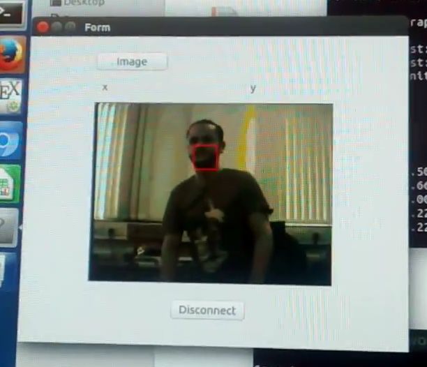
J. Imaging 2019, 5, 7                                                                              4 of 23

on-chip as rows, consuming precious processing time. Similarly, Chou et al. [26] have shown the
use of vector scratchpad memories for accelerating vector processing on FPGAs, but still rely on
random-access external memories; a similar approach is followed by Naylor et al. [27] in the context of
FPGAs as accelerators. The use of external memories solves the storage limitation: however, it greatly
limits parallelism (only one access per external memory chip can be performed at once) or greatly
exacerbates financial and power costs, if several external memories are used.

2.3. Partitioning Algorithms
      For HLS-based designs, computer vision algorithms are naturally expressed by assuming frames
are stored in unbounded address spaces [28]. This software approach to FPGA design not only easily
exceeds FPGA memory capabilities but is also not easily integrated in streaming designs without
significant refactoring. This has led to the development of custom hardware blocks and APIs for
software integration [29]: “naive” C-based HLS results in several on-chip memory structures, whose
sizes and interfaces are dependent on variables’ types, often sub-utilizing available on-chip memory.
Most HLS tools offer compiler directives—pragmas—which guide the synthesis tool according to
the designer’s intention: optimizing for performance through loop unrolling, or selecting different
implementations (on-chip memories or LUTs). We advocate that more directives, invoking different
synthesis strategies, are required in order to tackle design constraints such as space and power.
      The majority of research into partitioning algorithms has mainly focused on performance: namely,
throughput. Gallo et al. [30] have shown how to construct efficient parallel memory architectures
through High-Level Synthesis: however, their approach is predicated on re-organizing memory
placement at algorithm level, by examining computational behavior and placing data accordingly
through lattice-based partitioning, which is not feasible on streaming applications where pixels
are inputted sequentially. Although possible, it would require a complex memory addressing
mechanism between pixel input and memory structure. The authors then expanded their work
to incorporate information about loop unrolling [31], providing new partitioning algorithms for
maximizing parallelism; however, they did not tackle the utilization problem. Similarly, Wang et al. [32]
have demonstrated an extremely efficient algorithm for improving throughput, by creating memory
structures that facilitate loop pipelining in high level synthesis. Their approach saves up to 21%
of BRAMs compared to previous work [33]; still, since their objective is maximizing throughput,
supporting loop pipelining, their approach does not achieve optimized memory allocation in terms of
utilization efficiency.

2.4. Memory Power Reduction
     The impact of memory partitioning on power consumption has been researched by
Kadric et al. [34]. Their approach investigates the impact of parallelism, i.e., how data placement
can be leveraged for parallel access, minimizing communication power. A similar approach is taken
in [35]. Tessier et al. [36] show on chip memory power reduction through partitioning, similar to our
approach and previous work by the same authors [37], and more recently in [38]. However, none of
these investigations assume constraints on memory availability. In contrast, we investigate tradeoffs
between power and scarce availability, inherent to the image processing domain, future work need
clearly identified by Tessier et al: “an investigation to determine the optimal size and availability of
different-sized embedded memory blocks is needed".

3. Memory Partitioning on FPGA
      In this paper we describe how to partition image frames into BRAMs in order to maximize
utilization (i.e., minimize the number of required on-chip memories), subject to minimization of
power consumption. We begin by by formulating the utilization efficiency problem, without paying
any consideration to power aspects; the following section integrates power consumption in our
J. Imaging 2019, 5, 7 5 of 23
problem formulation. We assume that only one possible BRAM configuration is used for each image
frame buffer.
3.1. Problem Formulation: Utilization Efficiency
Definition 1. Given a BRAM storage capacity C, and a number of possible configurations i, the configurations
set Cfg is a vector of i elements:
( M1 , N1 ) Cfg1
( M , N ) Cfg
2 2 2
. .
Cfg = = (1)
. .
. .
( Mi , Ni ) Cfgi
where the first component of each element depicts BRAM width M and the second component depicts BRAM
height N, such that:
Mx × Nx ≤ C, ∀ x ∈ [0, i − 1] (2)
For any given frame size, several possible BRAM topologies are possible (Different BRAM
configurations do not always equal the same logical bit capacity. Whilst the total physical capacity is the
same, in some configurations parity bits can be used as additional data bits. E.g., configuration (1,16384)
can store 16384 bits, whilst configuration (9,2048) can store 18432 bits). A frame is a 3-dimensional array,
of dimensions width W, height H, and pixel bit width Bw (typically defined as a 2-dimensional array
where the type defines the bit width dimension). BRAM topologies are defined based on a mapping of
3-D to 2-D arrays and a partitioning of a 2-D array to a particular memory structure (Figure 1).
Figure 1. Mapping a 3-D array into row-major and colum-major order 2-D arrays.
J. Imaging 2019, 5, 7                                                                                         6 of 23

     Throughout the remainder of this paper, we assume the use of a mapping scheme which assigns
Bw to the x dimension and H and W to the y dimension, in both row-major and column-major
order (where x and y are 2-D array width and height, respectively). This is the default approach in
software implementations, where the type/bit width dimension is considered implicit, and a sensible
approach for hardware implementations. Mapping bit width Bw across the y dimension would result
in implementations where different bits of the same array element (pixel) would be scattered among
different memory positions of the same BRAM. This would require sequential logic to read/write a
pixel, accessing several memory positions, creating performance, power and size overheads. It should
be noted that this approach might offer performance advantages for certain classes of algorithms
which might want to compare individual bits of different elements; however, we delegate this aspect
to future work. Hence, we define only the default mapping scheme:

Definition 2. A mapping scheme m transforms a 3-D array A3 into a 2-D array A2 of dimensions x and y by
assigning Bw to the x dimension and ordered combinations of W and H to the y dimension, for a total of two
possible configurations, as depicted in Figure 1. Mapping schemes are defined as:

                                                           ( x, y) = m(W, H, Bw )                                (3)
                               A2x,y = A3y\W,y%W,x , x = Bw , y = W × H                                          (4)
                                A2x,y = A3y%H,y\ H,x , x = Bw , y = W × H                                        (5)

where \ and % represent integer division and modulo, respectively.

Definition 3. Given a 2-D mapped image frame of dimensions x and y, a partitioning scheme p which assigns
pixels across a × b BRAMs, depicted in Figure 2, is defined as the linear combination:

                                 p( x, y) = Cfg ∗ ( a1 , b1 ), ( a2 , b2 ), ..., ( ai , bi )                     (6)

where ∗ stands for linear combination, such that only one ( a x , bx ), ∀ x ∈ [0, i − 1] pair has non-zero components
(such a pair is generated as a function of x and y), selecting M p and Np subject to:

                                        (( a × M p ) ≥ x ) ∩ ((b × Np ) ≥ y)                                     (7)

      Figure 2. Mapping 2-D array of dimensions x = Bw and y = W × H to a × b BRAMs configured for
      width M and height N.

    Different partitioning schemes p, implementing different functions of x and y, result in different
addressing, input and output logic requirements, each with a particular impact on performance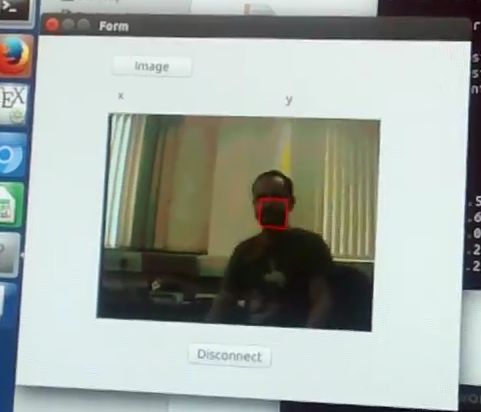
J. Imaging 2019, 5, 7 7 of 23
and resource usage. As this is the greatest bottleneck in implementing high-level image processing
pipelines on an FPGA, it is paramount to define BRAM usage efficiency, i.e., the ratio between the total
data capacity of the assigned BRAMs and the amount of data which is actually used.
Definition 4. Given a partitioning scheme p and maximum BRAM capacity C, the utilization efficiency E is
defined as the ratio:
x×y
E= (8)
a p × bp × C
The default mapping and partitioning schemes in state of the art HLS tools are geared towards
minimizing addressing logic (abundant in contemporary FPGAs), resulting in sub-par efficiency in
BRAMs usage (still scarce for the requirements of high-level image processing systems). Alternative
schemes must be used in order to ensure memory availability within HLS design flows. We define the
problem as:
Problem 1 (Utilization Efficiency). Given an image frame of width W, height H and pixel width Bw , select a
partitioning scheme, in order to:
x ×y
Maximize E = a p ×b p ×C
Subject to (( a × M p ) ≥ x ) ∩ ((b × Np ) ≥ y)
3.2. Utilization Example
Consider an image frame of width W = 320 and height H = 240, where each pixel is 8 bits
(monochrome), and BRAMs which can be configured according to:
(1, 16384)
(2, 8192)
(4, 4096)
Cfg = (9)
(9, 2048)
(18, 1024)
(36, 512)
which is representative of state of the art FPGAs (Xilinx Virtex 7 family 18Kbits BRAM.), where total
BRAM capacity C is given by C = 36 × 512. Using a partitioning scheme
T
(8, 8)
(0, 0)
(0, 0)
p(m(320, 240, 8)) = Cfg ∗ (10)
(0, 0)
(0, 0)
(0, 0)
where m(320, 240, 8) = (8, 76800) (Equation (3)), yields a BRAM usage count of 64 (8 × 8 BRAMs
configured for width 1 and height 16384), with storage efficiency:
8 × (320 × 240)
E= = 0.520833333 (11)
8 × 8 × (36 × 512)
We have observed that this is the default behaviour for Xilinx Vivado HLS synthesis tools:
empirical results show that configuration ( M1 , N1 ) = (1, 16384) is selected through a partitioning
scheme where a1 = Bw and
W×H
b1 = (12)
N1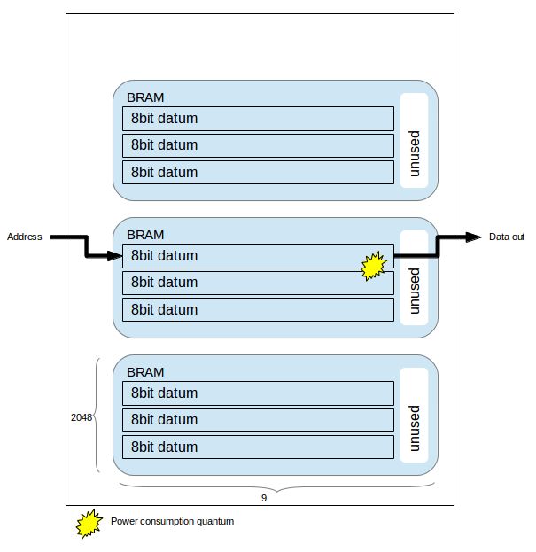
J. Imaging 2019, 5, 7 8 of 23
rounded up to the nearest power of 2. Our experiments show that for any frame size, the synthesis
tools’ default partitioning scheme can be given by:
T
dlog2 ( WN× H )e
( Bw , 2 1 )
(0, 0)
p(m(W, H, Bw )) = Cfg ∗ (0, 0)
(13)
(0, 0)
(0, 0)
(0, 0)
dlog ( W × H )e
where 2 2 N1 should be read as 2 to the rounded up (ceiled) result of the logarithm operation (i.e.,
2 to an integer power).
Now consider the same mapping (x = Bw , y = W × H), but with a partitioning scheme:
T
(8, 5)
(0, 0)
(0, 0)
p(m(320, 240, 8)) = Cfg ∗ (14)
(0, 0)
(0, 0)
(0, 0)
which partitions data unevenly across BRAMs, rather than evenly. This scheme yields a BRAM usage
count of 40, with storage efficiency:
320 × 240 × 8
E= = 0.833333333 (15)
8 × 5 × (36 × 512)
Yet a better partitioning scheme for the same mapping would be:
T
(0, 0)
(0, 0)
(2, 19)
p(m(320, 240, 8)) = Cfg ∗ (16)
(0, 0)
(0, 0)
(0, 0)
yielding a BRAM count of 38 and efficiency:
320 × 240 × 8
E= = 0.877192982 (17)
2 × 19 × (36 × 512)
Clearly, partitioning schemes depend on the frame dimensions, width, height, and bit width, to
enable efficient use of on-chip memory blocks.
3.3. Power Considerations
Having formalized the utilization problem, we may proceed to analyse the power implications
of each configuration. We model BRAM dynamic power consumption using the model described by
Tessier et al. [37]: a power quantum is consumed per read and/or write. BRAM static power is directly
proportional to utilization, hence addressed in the utilization problem.
For any given BRAM cell, the read power is consumed by a sequence of operations: the clock
signal is strobed; the read address is decoded; the read data is strobed into a column multiplexer; the
read data passes to BRAM external port. Write power is consumed by the following sequence: the
clock signal is strobed; the write enable signal transfers write data to the write buffers; a line is selected
by address decoding; data is stored in the RAM cell.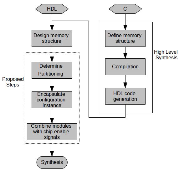
J. Imaging 2019, 5, 7                                                                               9 of 23

     Now consider the partitioning presented in Equation (10) where each datum is distributed across
eight BRAMs, and the partitioning presented in Equation (16), where each datum is distributed across
two BRAMs. Each read/write operation in the former must consume power across four times the
number of BRAMs in the latter. Figures 3 and 4 depict examples of power consumption for two
partitioning schemes.

Figure 3. Partitioning across two BRAMs horizontally. Each access consumes two power consumption quantums.

 Figure 4. Partitioning across one BRAM horizontally. Each access consumes 1 power consumption quantum.

      A partitioning scheme which minimizes horizontal usage of BRAMs (i.e., across x) is more suitable
for clock gating. Since fewer BRAMs must be accessed per operation, the proportian of unused ones,
which can be effectively gated, increases. It is straightforward to implement clock gating through chip
enable selection [39] which is enabled/disabled based on address decoding. colorred In other words,
BRAM power consumption is proportional to the number of BRAMs required to access each pixel: and
this number depends on which configuration is selected.
      An intuitive approach to balance power consumption and utilization is to always use the widest
BRAM configuration that suffices for Bw , or multiples of the widest available.
      This, however, is not an optimized strategy. While it is true that dynamic power is reduced, static
power might increase when moving from one configuration to a wider one since the total number of
J. Imaging 2019, 5, 7                                                                                                  10 of 23

BRAMs might increase: utilization efficiency is modified. Additionally, the logic required for address
(and chip enable) signals increases when moving to a wider configuration. This aspect makes the
utilization and power problems indivisible. In the following section, we describe our approach to
balance these two aspects.

3.4. Partitioning for Power and Utilization
      We begin by presenting a brute force optimized partitioning procedure for maximizing utilization
efficiency, described in Algorithm 1 in pseudo code notation.

Algorithm 1 Optimized Utilization Efficiency can be achieved by:
 1:   procedure O PTIMIZED PARTITION
 2:      efficiency ← 0
 3:      best ← 0
 4:      for x=0 : i-1 do
 5:           (Mx,Nx) ← Cfgx
 6:           a ← Bw/Mx
 7:           b ← W × H/Nx
 8:           efficiency ← (W × H × Bw)/( a × b × C )
 9:           if efficiency greater than best then
10:                best ← e f f iciency
11:                configuration ← ( Mx, Nx )
12:           end if
13:      end for

      For each element in the configurations set Cfg (possessing a total of i elements), the procedure
calculates the required number of BRAMs to store a frame of width W, height H and bit width Bw, the
efficiency of such a configuration and compares it with the highest efficiency found so far. The focus
here is solely on utilization. Effectively, this is an exhaustive search as the number of possible memory
configurations is finite and this is an off-line process.
      Table 1 depicts the configurations selected by procedure 1 for a representative number of frame
sizes and pixel bit widths. Several of the configurations are not power-optimised: notice that for pixels
of widths 10, 14 and 22, BRAM configuration 2 × 8192 is chosen most often (consuming power on 5, 7
and 11 BRAMs per access, respectively). This is intuitive from a utilization efficiency perspective: it is
the only configuration that divides the width, and is in accordance with the selection of configuration
4 × 4096 for pixels of width 8, 12, 20 and 24 and configuration 18 × 1024 for pixels of width 18.

                            Table 1. BRAM configurations based on optimized utilization procedure.

                                                                   Pixel Width
      Frame             8           10        12          14          16            18         20         22          24
    160 × 120     4 × 4096       4 × 4096   4 × 4096   18 × 1024   18 × 1024     18 × 1024   4 × 4096   9 × 2048   4 × 4096
    320 × 240     4 × 4096       2 × 8192   4 × 4096    2 × 8192   18 × 1024     18 × 1024   4 × 4096   2 × 8192    4 × 4096
    512 × 512     4 × 4096       2 × 8192   4 × 4096    2 × 8192    4 × 4096     18 × 1024   4 × 4096   2 × 8192   1 × 16384
    640 × 480     4 × 4096       2 × 8192   4 × 4096    2 × 8192   18 × 1024     18 × 1024   4 × 4096   2 × 8192    4 × 4096
   1280 × 720     4 × 4096       2 × 8192   4 × 4096    2 × 8192   18 × 1024     18 × 1024   4 × 4096   2 × 8192    4 × 4096

      This non-linearity complicates the derivation of an optimized procedure for partitioning for both
utilization and power efficiencies. Hence, we take a more relaxed approach and define a procedure
through user defined tradeoffs (i.e., an estimation of how much BRAM utilization can be traded
for power reduction) and power and space heuristics, based on empirical properties. Our brute
force balanced method is described in Algorithm 2. It is assumed that the tradeoff is expressed in
percentage points.
J. Imaging 2019, 5, 7 11 of 23
Algorithm 2 Balanced Power-Utilization can be achieved by:
1: procedure B ALANCED PARTITION
2: efficiency ← 0
3: configuration ← get_MxNx(OptimizedPartition())
4: best ← get_efficiency(OptimizedPartition())
5: j ← get_index(OptimizedPartition())
6: for x=j+1 : i-1 do efficiency
7: (Mx,Nx) ← Cfgx
8: a ← Bw/Mx
9: b ← W × H/Nx
10: efficiency ← (W × H × Bw)/( a × b × C )
11: if efficiency less than best - tradeoff then
12: break
13: end if
14: configuration ← ( Mx, Nx )
15: end for
Procedure 2 begins by selecting the optimized utilization solution and iterating over wider BRAM
configurations (in the x dimension), calculating utilization efficiency. As long as the utilization is
above the threshold limit, given by the difference between best utilization and tradeoff, in percentage
points, the procedure continues. When it finds the first solution below the threshold, it exits, returning
the last solution above the threshold limit. This approach follows the power model heuristics [37]
described in the previous section: power consumption decreases as BRAM horizontal width increases
(Figures 3 and 4).
Table 2 depicts the BRAM configurations selected by the balanced procedure, with the tradeoff
set to 12 percentage points. Compared to the optimized configurations, the majority of widths are
increased, resulting in a more power efficient solution based on the aforementioned heuristics.
Table 2. BRAM configurations based on balanced procedure with tradeoff equal to twelve percentage
points.
Pixel Width
Frame 8 10 12 14 16 18 20 22 24
160 × 120 9 × 2048 4 × 4096 4 × 4096 18 × 1024 18 × 1024 18 × 1024 4 × 4096 9 × 2048 9 × 2048
320 × 240 9 × 2048 4 × 4096 4 × 4096 18 × 1024 18 × 1024 18 × 1024 4 × 4096 9 × 2048 9 × 2048
512 × 512 9 × 2048 2 × 8192 4 × 4096 18 × 1024 18 × 1024 18 × 1024 4 × 4096 9 × 2048 9 × 2048
640 × 480 9 × 2048 2 × 8192 4 × 4096 18 × 1024 18 × 1024 18 × 1024 4 × 4096 9 × 2048 9 × 2048
1280 × 720 9 × 2048 2 × 8192 4 × 4096 18 × 1024 18 × 1024 18 × 1024 4 × 4096 9 × 2048 9 × 2048
3.5. Applying Memory Partitioning: Methodology
Our procedures can be utilized in both HDL and HLS design flows: in an HDL design flow,
by guiding the designer’s implementation and/or refactoring; in an HLS design flow, through
integration in the synthesis tools code generation subsystem. Figure 5 depicts the proposed design
flows. The additional steps can be performed manually, either starting from HDL designs or by
modifying HLS outputs pre-synthesis; through automated refactoring tools which compute the
proposed procedures; or by the HLS tool prior to code generation. We describe the manual process
used in our experiments.J. Imaging 2019, 5, 7 12 of 23
Figure 5. Proposed design flow from HDL and HLS, highlighting the additional steps required for
minimizing utilization and power.
After a memory structure has been derived from the procedure specification, according to
Equations (3)–(5), procedures 1 and/or 2 are computed to determine BRAM partitioning. BRAMs of
the computed configuration are instantiated and contained in modules (i.e., hardware entities). A top
module instantiates all sub-modules, providing interfaces identical to the base HDL design or to the
specification of the HLS tool. Addressing logic within the top module controls chip enable signals to
each sub-module, ensuring that non-addressed BRAMs are not enabled. This careful partitioning of
HDL logic in hierarchical modules, where addressing logic is determined by the top-level interconnect
and BRAM configuration is determined by module configuration parameters ensures that the desired
configurations are used (this is based on our experiments using Vivado: different synthesis tools might
require additional compiler pragmas).
4. Experimental Results
Our experiments target state of the art FPGA devices (Xilinx Virtex 7 device xc7vx690tffg1761-1C
and Zynq xc7z020clg484-1). We use Vivado v2016.1 for HDL design, Vivado HLS v2016.1 for High
Level Synthesis, and Xilinx Power Estimator for power characterization of implemented designs.
We begin by generating frame buffers in several configurations, in order to characterise utilization
efficiency and power consumption. We then compare utilization and power against equivalent frame
buffers generated by a HLS tool. We conclude by implementing two high level image processing
algorithms through HLS, and modifying frame buffers according to the proposed strategies, in order
to quantify our algorithms’ impact on resource usage and power consumption within complete image
processing systems.
4.1. Frame Buffers: BRAM Configuration Impact
Our first set of experiments characterises utilization and power consumption for two frame
sizes as a function of several possible configurations. The goal of this set of experiments was to
validate the utilization efficiency of the partitioning algorithms and the power heuristics used in the
previous section.J. Imaging 2019, 5, 7 13 of 23
We implemented frame buffers in Verilog HDL in Vivado v2016.1, explicitly instantiating BRAMs
according to the desired configurations. Logic in our design hierarchy routes data, addresses and
control signals accordingly. Analysis of post-implementation reports was performed in order to
ensure that BRAMs were instantiated according to the desired configuration (depending on the design
hierarchy, synthesis tool optimizations could feasibly re-organize BRAM allocation). We performed
a sequential read/write experiment, where a complete frame is written to memory (sequential pixel
input, in row-major order) and then read in the same order. This allows us to validate the power
model heuristics assumed in the previous section. Table 3 depicts power and utilization results for
monochrome frames of sizes 320 × 240 and 512 × 512.
Table 3. FPGA power usage and utilization efficiency (Eff.) for monochromatic (8 bits) frames of sizes
320 × 240 and 512 × 512 for different BRAM configurations.
320 × 240 512 × 512
Power (W) Power (W)
Configuration Eff. (%) Configuration Eff. (%)
Static Dynamic BRAM Static Dynamic BRAM
8 × 5–1 × 16384 0.328 0.054 0.036 83.33 8 × 16–1 × 16384 0.332 0.07 0.036 88.88
4 × 10–2 × 8192 0.327 0.036 0.018 83.33 4 × 32–2 × 8192 0.331 0.053 0.018 88.88
2 × 19–4 × 4096 0.327 0.026 0.009 87.72 2 × 64–4 × 4096 0.331 0.043 0.009 88.88
1 × 38–9 × 2048 0.327 0.027 0.005 87.72 1 × 128–9 × 2048 0.331 0.046 0.005 88.88
4.2. Frame Buffers: HLS Comparison
Our second set of experiments compares the proposed partitioning algorithms with default
strategies employed by commercial HLS tools. The goal of this set of experiments was to confirm
that the proposed methodology outperforms commercial HLS tools in both utilization and power
consumption.
We performed C-based high level synthesis using Xilinx Vivado HLS, describing frames in the
standard format (array type determines bit width, indices determine frame width and height). For each
frame size, we report BRAM usage and additional resources (slice registers and LUTs). We utilized
standard pixel widths (8 bits for monochrome images, 24 bits for RGB). We estimated optimized
BRAM usage using the optimized utilization algorithm and according to the balanced partitioning
algorithm in order to compare the power and utilization impact—algorithms were run offline; we
have not integrated them in any HLS tool at this point. We implemented the frame buffers in Verilog
HDL according to each algorithm, ensuring external interfaces (i.e., read/write data, address and
control singals ports) are identical to the ones generated by Vivado HLS from C. We then replaced
the frame buffers generated from HLS with our hand-coded Verilog HDL versions. For each frame
size, we report BRAM usage and additional resources (slice registers and LUTs) required to implement
addressing logic.
Table 4 depicts results obtained from the three configurations, for monochromatic and RGB
frames respectively, and Figure 6 compares BRAM utilization efficiency. We characterised the power
consumption implications of each generated system using Xilinx Power Estimator for access patterns
representative of image processing applications. In our sequential read/write experiment, a complete
frame is written to memory (sequential pixel input, in row-major order) and then read in the same
order. In our sliding window experiment, a complete frame is read through 3 × 3 sliding window.
Figure 7 depicts static power consumption; Figures 8 and 9 depict total dynamic power consumption
by the three architectures, for sequential read/write and sliding window test cases, respectively; and
Figures 10 and 11 depict BRAM power consumption for sequential read/write and sliding window test
cases, respectively.J. Imaging 2019, 5, 7 14 of 23
Table 4. FPGA resource usage for monochromatic frames: generated from Vivado HLS versus
hand-coded modifications according to the proposed algorithms.
8 bits HLS Optimized Utilization Balanced
BRAMs BRAMs
Frame BRAMs LUTs LUTs LUTs
Usage Mode Reduction Usage Mode Reduction
160 × 120 16 0 10 4 × 4096 −37.5% 22 10 9 × 2048 −37.5% 48
320 × 240 64 9 38 4 × 4096 −40.6% 79 38 9 × 2048 −40.6% 186
512 × 512 128 17 128 4 × 4096 0% 285 128 9 × 2048 0% 596
640 × 480 256 34 150 4 × 4096 −41.4% 337 150 9 × 2048 −41.4% 742
1280 × 720 512 64 450 4 × 4096 −12.1% 1039 450 9 × 2048 −12.1% 2284
24 bits HLS Optimized Utilization Balanced
BRAMs BRAMs
Frame BRAMs LUTs LUTs LUTs
Usage Mode Reduction Usage Mode Reduction
160 × 120 48 0 30 4 × 4096 −37.5% 41 30 9 × 2048 −37.5% 91
320 × 240 192 25 114 4 × 4096 −40.6% 140 114 9 × 2048 −40.6% 308
512 × 512 384 49 384 1 × 16384 0% 504 384 9 × 2048 0% 1109
640 × 480 768 98 450 4 × 4096 −41.4% 584 450 9 × 2048 −41.4% 1285
1280 × 720 1536 192 1350 4 × 4096 −12.1% 1760 1350 9 × 2048 −12.1% 3877
Figure 6. BRAM utilization efficiency for RGB frames: Vivado HLS versus proposed methods.
Figure 7. Static power consumption: Vivado HLS versus proposed methods.J. Imaging 2019, 5, 7 15 of 23
Figure 8. Total dynamic power consumption for sequential read/write: Vivado HLS versus proposed methods.
Figure 9. Total dynamic power consumption for 3 × 3 sliding window read: Vivado HLS versus
proposed methods.
Figure 10. BRAM power consumption for sequential read/write: Vivado HLS versus proposed methods.J. Imaging 2019, 5, 7 16 of 23
Figure 11. BRAM power consumption for 3 × 3 sliding window read: Vivado HLS versus proposed methods.
4.3. High-Level Image Processing
Out third set of experiments contextualises the impact of memory allocation on high-level image
processing systems. The goal of this set of experiments was to quantify how much frame buffers
impact resource usage and power consumption within complete image processing systems, based on
default and proposed partitioning strategies.
We use Optical Flow and MeanShift Tracking as case studies. Optical Flow estimates the apparent
motion of objects caused by the relative motion of an observer; i.e., for two sequential frames, Optical
Flow estimates the movement of each pixel (or larger regions) from one frame to the other. It belongs
to the temporal class of image processing algorithms, i.e., it performs computations across time
(different frames). Our Optical Flow implementation is based on the code available from [40] using the
TV-L1 method, refactored so it complies with Vivado HLS C synthesis requirements (e.g., dynamic
memory allocation was replaced by static memory allocation); we performed no other optimizations.
We compute a single scale, rather than multiple scales, for images of size 160 × 120: an example is
depicted in Figure 12. We used the publicly available dataset from [41]. We developed three versions:
with default memory allocation and following the optimized utilization and balanced algorithms.
FPGA utilization results for Xilinx Virtex 7 are depicted in Table 5 (optimized and balanced strategies
yield the same BRAM utilization, although different configurations, for our implementation). For the
default strategy, BRAMs were insufficient to accommodate all memory requirements, causing the
synthesis tool to infer Memory LUTs for parts of the design. Using our approach, BRAMs suffice to
implement the complete system. Power consumption per version is depicted in Figure 13.
Table 5. Optical Flow FPGA resource usage and performance on Virtex 7 xc7vx690tffg1761-1: generated
from Vivado HLS versus hand-coded modifications according to the proposed algorithm.
Vivado HLS Default Optimized
FF 24101 (3%) 24101 (3%)
LUTs 200205 (47%) 208724 (49%)
Memory LUT 126114 (73%) -
IOs 568 (67%) 568 (67%)
BRAM 1008 (35%) 2157 (74%)
DSPs 232 (7%) 232 (7%)
fps 24 24J. Imaging 2019, 5, 7 17 of 23
(a) First frame (b) Second frame
(c) 1 scale optical flow (d) 5 scales optical flow
Figure 12. Optical Flow results using the implementation from [40]. (a,b): source frames. (c): output
from 1 scale optical flow (used in our FPGA implementation). (d): output from 5 scales optical flow.
Figure 13. TV-L1 Optical Flow power consumption on Virtex 7.
MeanShift Tracking [24] calculates a confidence map for object position on an image, based on
a colour histogram of such object on a previous image: i.e., for an object whose position is known
and colour histogram is calculated in frame k, MeanShift Tracking determines the most likely object
position in frame k + 1, based on colour histogram comparison. It is a temporal and dynamic algorithm:
it performs computations across more than one frame, requiring an unpredictable number of iterations
(up to a predefined maximum) on unpredictable frame positions (depending on runtime object
position). It was described in C and implemented through Vivado HLS; our implementation was
highly optimized for hardware implementation. MeanShift Tracking stores the first input frame
(writing the full frame to memory in sequential, row-major order) and calculates a color histogram
of a region of width M and height N, centered on an initial object position (reading M × N pixels).
Every subsequent frame is stored, and color histograms for possible new positions are calculated in a
region around the previous known position. The new position is decided when the difference between
previous and current position is below a pre-defined error bound or a maximum number of iterations
is reached. The MeanShift tracking access patterns are not regular or predictable as they depend on
the input images; it is representative of memory-intensive image processing algorithms as the output
depends on complete (or unpredictable subsets of) scenes, rather than well-defined pixels or regions.
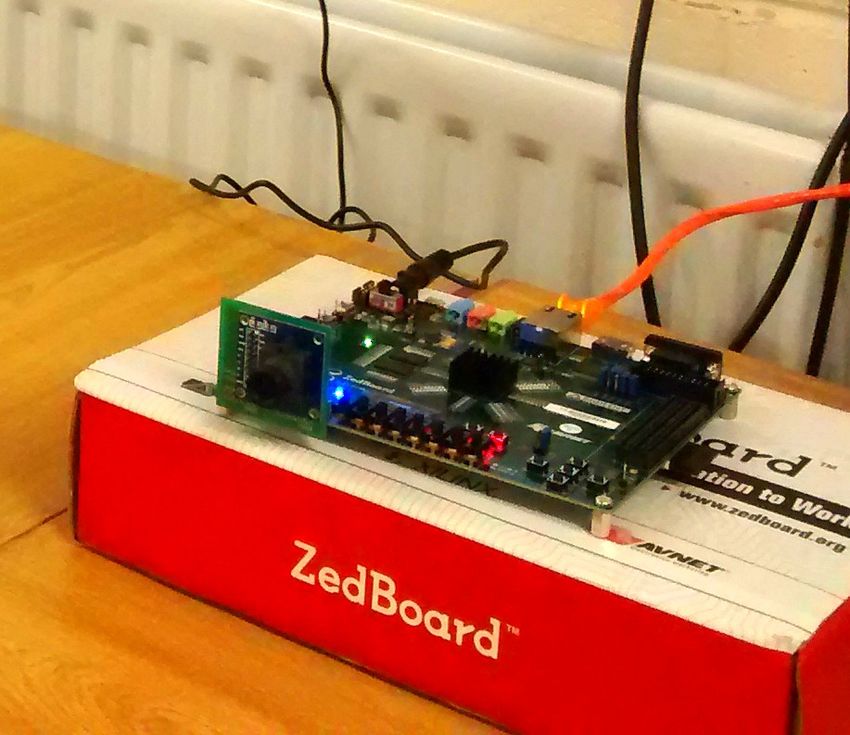
Our tracking system was implemented on a Zynq 7020 chip on a Zedboard, connected to an
external camera OV7670 (Figure 14). The processed data (image plus tracked object position) are
sent to the on-board ARM processor which re-transmits to a remote desktop computer over Ethernet.
However, it is important to stress that this for communication and display only, the complete algorithm
is implemented on the FPGA. Figure 15 shows real-time operation of our setup.J. Imaging 2019, 5, 7 18 of 23
Figure 14. Zedboard connected to PC through Ethernet.
Figure 15. MeanShift Tracking: real-time face tracking displayed on PC. Image sent from Zedboard
over Ethernet connection.
We developed three system versions: with default memory allocation, optimized utilization
memory allocation and balanced allocation for image sizes of 320 × 240 where each pixel is 24 bits
(RGB), with a region of interest of size M = 16 and N = 21. Identical to the previous experiment,
our baseline is the MeanShift Tracking implementation generated by Vivado HLS. The versions used
for comparison replace the HLS frame buffer with hand-coded implementations: all other MeanShift
Tracking modules are unmodified (generated from C through Vivado HLS). Resource usage for each
version is depicted in Table 6. Power consumption per version is depicted in Figure 16.
Table 6. MeanShift Tracking FPGA resource usage and performance on Zynq 7020: generated from
Vivado HLS versus hand-coded modifications according to the proposed algorithms.
Vivado HLS Default Optimized Balanced
FF 6264 (5%) 6264 (5%) 6264 (5%)
LUTs 9197 (17%) 9310 (17.5%) 9475 (17.8%)
IOs 64 (32%) 64 (32%) 64 (32%)
BRAM 228 (81%) 150 (54%) 150 (54%)
DSPs 8 (3%) 8 (3%) 8 (3%)
fps 134 134 134J. Imaging 2019, 5, 7 19 of 23
Figure 16. MeanShift Tracking power consumption on Zedboard.
5. Discussion of Results
Regarding the experiments in Section 4.1, we purposely chose these configurations in order to
highlight the non-linear relationship between efficiency and power; while for frames of size 320 × 240,
different configurations yield different efficiency and different power consumption, efficiency is
identical across configurations for frames of size 512 × 512, while power consumption still varies. It is
worthwhile noticing that for both sizes, BRAM configuration 9 × 2048 is less power efficient than
configuration 4 × 4096, despite achieving the same efficiency; although BRAM power is decreased
(from 0.009 W to 0.005 W in both cases), total dynamic power (comprised of BRAM, clocks, signals,
logic and I/O) increases due to more complex logic, as previously described.
Experiments show that our partitioning algorithms achieve higher efficiency than default synthesis
strategies, except for frames of size 512 × 512 where the efficiency is unchanged. This is the case
where default strategies perform equally well in terms of utilization since the image height and width
are powers of 2 (refer back to Equation (13)). This confirms that modified partitioning strategies are
required, according to requirements, in order to improve memory usage.
Static power consumption depicted in Figure 7 decreases across frame sizes, except for frames
of sizes 512 × 512 and 1280 × 720, where the utilization efficiency difference between default and
proposed strategies is smallest (Figure 6) and additional addressing logic becomes too (static) power
hungry. This confirms the utilization and power problems are indivisible, and must be treated
in synergy.
Total dynamic power, on experiments performed on frame buffers, is reduced on average by
74.708% (σ = 7.819%) for read/write experiments (Figure 8), and on average by 72.206% (σ = 12.546%)
for read-only experiments (Figure 9). This confirms our hypothesis that memory partitioning offers
opportunities for power reduction, despite the need for logic overhead. Considering BRAM dynamic
power only, our partitioning methods result in 95.945% average power reduction (σ = 1.351%) for
read/write experiments (Figure 10) and 95.691% average power reduction (σ = 1.331%) for read-only
experiments (Figure 11).
On our experiments using Optical Flow, where BRAM and Memory LUT power accounts for
25.9% of total power consumption, and 30% of dynamic power, we show that the proposed partitioning
algorithms can reduce total power by approximately 25% (Figure 13). For MeanShift Tracking, where
BRAM power accounts for 34.55% of total power consumption, and 53.94% of dynamic power, we show
that the proposed partitioning algorithms can reduce total power by approximately 30% (Figure 16).
Algorithm performance (i.e., frames per second) was unaffected by our partitioning methodologies,
both in Optical Flow and MeanShift Tracking, since our strategies do not affect memory access latencies
and maximum clock frequencies remained unchanged (frame buffers were not responsible for clock
critical path). Our results compare favorably to the results presented in [36], which achieved up toJ. Imaging 2019, 5, 7 20 of 23
26% BRAM power reduction, at the expense of 1.6% clock frequency reduction; our methodology
achieves up to 74% BRAM power reduction, without sacrificing clock frequency. This is due to the fact
that their approach does not consider the power consumption differences caused by different BRAM
configurations, a key aspect of our methodology.
5.1. Power Consumption
In Section 3.3, we illustrated how different BRAM configurations affect power consumption:
depending on how many BRAMs must be strobed in order to access a pixel (in other words, depending
on which configuration is used for memory allocation), different power consumption quanta are
expended (assuming the remaining ones are clock gated, as per our methodology). The interested
reader may refer to [37] for a detailed explanation of this power model. Figures 3 and 4 visually
display this phenomenon. Table 4 showed how, for the same frame size, different configurations can
reduce power consumption expended on BRAMs by up to 82%; this corresponded to total dynamic
power reduction of up to 50%. These results showed how severely BRAM configuration affects power
consumption. Note that it is possible that a very small reduction in BRAM utilization (i.e., the number
of BRAMs required to implement frame storage) can yield substantial power reductions.
In our experiments using complex high level algorithms, we showed that BRAM power constitutes
a substantial portion of total power consumption: namely, using the default Vivado HLS strategy,
BRAMs account for 8% of Optical Flow power consumption and 34% of Meanshift Tracking power
consumption (Figures 13 and 16). Additionally, significant power is spent on logic due to BRAM
output change (prevented in our approach due to clock gating strategies).
5.2. Hardware Overhead
The default memory allocation strategy employed by HLS tools appears to be focused on
minimizing addressing logic (implemented through LUTs), at the expense of memory usage. In contrast,
our approach minimizes memory usage (a scarcer resource than LUTs) at the expense of more complex
addressing. i.e., due to the use of different BRAM configurations, memory control logic (write-enable
signals, address decoding, etc.) becomes slightly more complex, consuming more LUTs to implement.
In our experiments using high level algorithms (Meanshift tracking and Optical Flow), this LUT
overhead was of 0.8 and 2.0 percentage points, respectively (see Tables 5 and 6).
6. Conclusions
Efficient mapping of high-level descriptions of image frames to low-level memory systems is an
essential enabler for the widespread adoption of FPGAs as deployment platforms for high-level image
processing applications. Partitioning algorithms are one of the design techniques which provide routes
towards power-and-space efficient designs which can tackle contemporary application requirements.
Based on a formalization of BRAM configuration options and a memory power model, we have
demonstrated how partitioning algorithms can outperform traditional strategies in the context of High
Level Synthesis. Our data show that the proposed algorithms can result in up to 60% higher utilization
efficiency, increasing the sizes and/or number of frames that can be accommodated on-chip, and reduce
frame buffers dynamic power consumption by up to approximately 70%. In our experiments using
Optical Flow and MeanShift Tracking, representative high-level image processing algorithms, data
show that partitioning algorithms can reduce total power by up to 25% and 30%, respectively, without
any performance degradation. Our strategies can be applied to any FPGA family and can easily scale
as required for future FPGA platforms with novel on-chip memory capabilities and configurations.
The majority of HLS design techniques have focused on programmability and performance.
However, our results show that further research is required in order to improve design strategies
towards accommodating other constraints; namely, size and power. Models which describe low-level
non-functional properties such as power consumption can support high-level constructs in order
to display early cost estimation, guiding the design flow. This requires not only fine-grainedJ. Imaging 2019, 5, 7 21 of 23
characterization of technologies’ properties, but also sufficiently powerful modeling abstractions which
can lift these properties to high-level descriptions. It will also be interesting to profile and refactor
image processing algorithms to determine if alternative mappings (refer back to Equations (4) and (5))
could provide higher performance and utilization; this could be pursued in future work involving
multi-objective optimizations.
Research in FPGA dynamic reconfiguration has focused on overcoming space limitations; whether
this capability can be exploited for image processing power reduction, based on heuristics and runtime
decisions, essentially transforming approximate computing design from a static to a dynamic paradigm,
remains an open question.
Author Contributions: Conceptualization and methodology, P.G. and D.B.; methodology and software, P.G. and
R.S.; validation, P.G., R.S. and A.W.; writing—original draft preparation, P.G., D.B.and A.W.; writing—review and
editing, A.W. and G.M.; project administration and funding acquisition, A.W. and G.M.
Funding: We acknowledge the support of the Engineering and Physical Research Council, grant references
EP/K009931/1 (Programmable embedded platforms for remote and compute intensive image processing
applications) and EP/K014277/1 (MOD University Defence Research Collaboration in Signal Processing).
Conflicts of Interest: The authors declare no conflict of interest. The funders had no role in the design of the
study; in the collection, analyses, or interpretation of data; in the writing of the manuscript, or in the decision to
publish the results.
References
1. Wang, J.; Zhong, S.; Yan, L.; Cao, Z. An Embedded System-on-Chip Architecture for Real-time Visual
Detection and Matching. IEEE Trans. Circuits Syst. Video Technol. 2014, 24, 525–538. [CrossRef]
2. Mondal, P.; Biswal, P.K.; Banerjee, S. FPGA based accelerated 3D affine transform for real-time image
processing applications. Comput. Electr. Eng. 2016, 49, 69–83. [CrossRef]
3. Wang, W.; Yan, J.; Xu, N.; Wang, Y.; Hsu, F.H. Real-Time High-Quality Stereo Vision System in FPGA.
IEEE Trans. Circuits Syst. Video Technol. 2015, 25, 1696–1708. [CrossRef]
4. Jin, S.; Cho, J.; Pham, X.D.; Lee, K.M.; Park, S.K.; Kim, M.; Jeon, J.W. FPGA Design and Implementation of a
Real-Time Stereo Vision System. IEEE Trans. Circuits Syst. Video Technol. 2010, 20, 15–26.
5. Perri, S.; Frustaci, F.; Spagnolo, F.; Corsonello, P. Design of Real-Time FPGA-based Embedded System for
Stereo Vision. In Proceedings of the 2018 IEEE International Symposium on Circuits and Systems (ISCAS),
Florence, Italy, 27–30 May 2018; pp. 1–5.
6. Schlessman, J.; Wolf, M. Tailoring design for embedded computer vision applications. Computer 2015,
48, 58–62. [CrossRef]
7. Stevanovic, U.; Caselle, M.; Cecilia, A.; Chilingaryan, S.; Farago, T.; Gasilov, S.; Herth, A.; Kopmann, A.;
Vogelgesang, M.; Balzer, M.; Baumbach, T.; Weber, M. A Control System and Streaming DAQ Platform with
Image-Based Trigger for X-ray Imaging. IEEE Trans. Nucl. Sci. 2015, 62, 911–918. [CrossRef]
8. Dessouky, G.; Klaiber, M.J.; Bailey, D.G.; Simon, S. Adaptive Dynamic On-chip Memory Management for
FPGA-based reconfigurable architectures. In Proceedings of the 2014 24th International Conference on Field
Programmable Logic and Applications (FPL), Munich, Germany, 2–4 September 2014; pp. 1–8.
9. Torres-Huitzil, C.; Nuño-Maganda, M.A. Areatime Efficient Implementation of Local Adaptive Image
Thresholding in Reconfigurable Hardware. ACM SIGARCH Comput. Arch. News 2014, 42, 33–38. [CrossRef]
10. Appuswamy, R.; Olma, M.; Ailamaki, A. Scaling the Memory Power Wall With DRAM-Aware Data
Management. In Proceedings of the 11th International Workshop on Data Management on New Hardware,
Melbourne, Australia, 31 May–4 June 2015; p. 3.
11. Memik, S.O.; Katsaggelos, A.K.; Sarrafzadeh, M. Analysis and FPGA implementation of image restoration
under resource constraints. IEEE Trans. Comput. 2003, 52, 390–399. [CrossRef]
12. Jiang, H.; Ardo, H.; Owall, V. A Hardware Architecture for Real-Time Video Segmentation Utilizing Memory
Reduction Techniques. IEEE Trans. Circuits Syst. Video Technol. 2009, 19, 226–236. [CrossRef]
13. Baskin, C.; Liss, N.; Zheltonozhskii, E.; Bronstein, A.M.; Mendelson, A. Streaming architecture for large-scale
quantized neural networks on an FPGA-based dataflow platform. In Proceedings of the 2018 IEEE
International Parallel and Distributed Processing Symposium Workshops (IPDPSW), Vancouver, BC, Canada,
21–25 May 2018; pp. 162–169.You can also read