Porous Silicon Optical Biosensors: Still a Promise or a Failure?
←
→
Page content transcription
If your browser does not render page correctly, please read the page content below
sensors
Opinion
Porous Silicon Optical Biosensors: Still a Promise or
a Failure?
Luca De Stefano
 Institute for Microelectronics and Microsystems, National Research Council, Via P. Castellino 111,
 80131 Napoli, Italy; luca.destefano@cnr.it

 Received: 3 October 2019; Accepted: 1 November 2019; Published: 3 November 2019

 Abstract: Even if the first published article on a porous silicon (PSi)-based biosensor dates back to
 more than twenty years ago, this technology still attracts great attention from many research groups
 around the world. In this brief review, the pros and cons of porous silicon-based optical biosensors
 will be highlighted on the basis of some recent results and published papers on this subject. The
 aim of the paper is to give a straightforward introduction to PhD students and young researchers
 on this subject, which is particularly full of educative content, since it is highly multidisciplinary.
 Fabrication of PSi-based optical biosensors requires competencies related to many different scientific
 topics ranging from material science, physics and optics to healthcare and environmental monitoring
 through surface chemistry and more.

 Keywords: porous silicon; optical biosensors; functionalization; label-free imaging

1. Introduction
       When I was offered the chance to give a lecture on optical biosensors based on porous silicon (PSi)
at the prestigious ASCOS 2019 school, dedicated to optical biosensing for life science and environmental
applications, I immediately asked myself if the topic, as well as being one I was really confident in, was
innovative enough to be presented properly to an audience of students from all over the world. This
doubt arose from the observation that the first article on PSi-based optical biosensors was published
more than twenty years ago [1], and it was therefore legitimate to ask myself the question as to whether
this argument was still relevant. The answer was that it was certainly worth, it given the large interest
that this technology still arouses in many laboratories scattered all over the world, from Europe to
Australia, from China to America. In the last five years, more than 400 scientific papers have been
published dedicated to optical sensors in porous silicon in peer-review journals (number estimated by
Scopus, accessed in July 2019); a number that is not very high in absolute terms, but which testifies to
the liveliness of the scientific community in relation to this topic.
       PSi is fabricated by the electrochemical dissolution of doped crystalline silicon using a
hydrofluoric-based water solution. The dissolution of the silicon is mediated by the charge carriers,
i.e., the electrons and holes, and proceeds from the surface in contact with the solution down by
a self-stopping mechanism, so that complex multi-layered structures can be realized by a single
computer-controlled etching procedure without touching the sample. All these steps are clearly
described in the recent book by Prof. M.J. Sailor at the University of California San Diego, USA, which
leads one of the most active groups in PSi-based research topics [2]. On the webpage of Sailor’s
group, there are also illustrative videos on PSi fabrication and characterization [3]. The realization of
optical PSi structures could be considered simple, but it is not trivial, and a lot of attention should
be paid in order to obtain regular and repeatable devices with high performance capabilities. The
porosity is one of the main characteristics of PSi films. Porosity is defined as the amount of void in
a solid layer, and it is related to the number and the size of the pores created by the dissolution of

Sensors 2019, 19, 4776; doi:10.3390/s19214776                                      www.mdpi.com/journal/sensors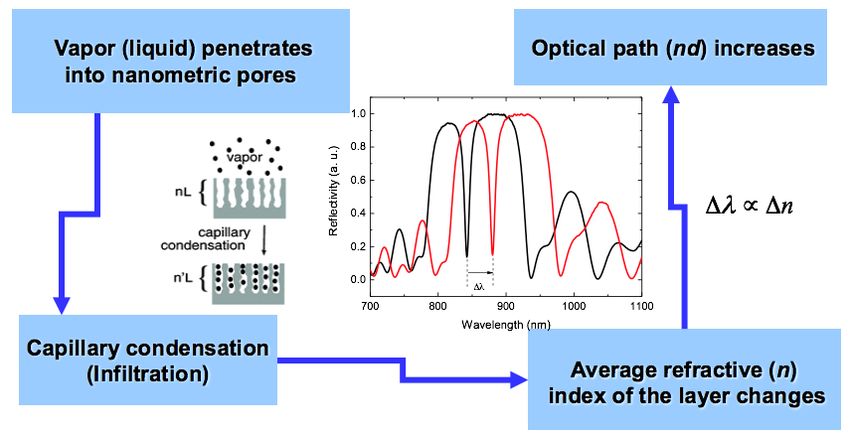
Sensors 2019, 19, 4776                                                                                2 of 8

the bulk silicon. In principle, its value could range between 0 (no dissolution of crystalline silicon)
and 1 (all air). By tuning the porosity during the electrochemical etching, by changing the time
length and the current flowing into the cell, the refractive index of a PSi layer can be changed from
that of the silicon (more than approximately 3.88 in the visible wavelength interval) to that of air (1,
by definition). Simple homogeneous PSi layers, as well as very complex multilayered ones, such
as Fibonacci and Thue-Morse sequences, can be realized just by writing different “recipes” for the
computer-aided voltage controller [4,5]. Similar optical structures could of course be realized by classic
micro/nanofabrication techniques, such as those for thin film deposition, i.e., chemical vapor deposition
and correlated processes. However, the optical feature is not the only one required in a transducer
material for sensing applications. There are many other issues that must be correctly addressed. In the
following, the main pros and cons of PSi as a nanostructured material for optical biosensors will be
considered and critically analyzed.

2. The Pros of PSi-Based Optical Biosensors
      An optical transducer is, by definition, a device made of a material that is light active. This means
that, after the molecular interaction between the probe and the target, some feature of the light coming
from or through the transducer changes as much as possible. The absorption, the phase, the intensity,
or whatever other property of the propagating light is therefore monitored and correlated with the
biomolecular event under investigation. The greater the variation, the better the transducer. Things
work even better if there is a resonance in the optical spectrum; for example, a peak in the absorbance
or a dip in the transmittance. A narrow resonance is simpler to follow during the evolution of the
optical signal, and thus the sensitivity of the method could increase. All optical and photonic devices
for biosensing are designed so that the sensitivity is maximized, and the limit of detection can be as
low as possible [6]. The realization of resonant photonic structures based on crystalline silicon or III-V
semiconductors requires accurate numerical calculation and the best of the available technologies
for micro- and nano-fabrication. Moreover, all of this instrumentation must be placed in a special
environment, i.e., a clean room, where temperature, humidity and dust concentration are carefully
controlled. All of these restrictions have made integrated photonic devices for biosensing available to
only few teams around the world, and at costs that are unsustainable for small research groups. PSi
photonic structures can be fabricated under a chemical hood even outside a clean room, with a simple
electrochemical cell and a current-voltage controller. The investment required for this equipment is
within the reach of almost all laboratories that deal with material science. Furthermore, the technical
skills for PSi fabrication can be learned by anyone with a minimal background in chemistry [7], even if
the handling of HF, which is a very dangerous substance, requires a proper specific course of instruction
regarding safe practice with this reagent. High-sensitivity PSi optical sensors have recently been
published by the group of Prof. G. Barillaro at the University of Pisa, Italy [8,9]. The PSi-based photonic
crystal realized demonstrated a sensitivity of 1000 nm/refractive index unit, which was able to compete
with the better-integrated optical devices, such as nanorings or nanopillars. Its low cost and simple
(but not trivial) fabrication procedures are certainly pros in favor of PSi.
      How does a PSi optical transducer work? Figure 1 shows a simple scheme for this
well-known mechanism.
Sensors 2019, 19, 4776 3 of 8
Sensors 2019, 19, x FOR PEER REVIEW 3 of 8
Figure 1. Schematic
Schematic representation
representation of
of PSi
PSi sensing
sensing mechanism
mechanism based
based on
on the variation
variation of the average
refractive index.
Every substance
Every substance that
that penetrates
penetrates into into the
the sponge-like
sponge-like matrixmatrix of of a PSi layer changes its average
refractive index so that the optical spectrum also changes. The The shift
shift of
of the
the optical
optical spectrum depends depends
parameters, one
on two parameters, one being
being the
the pore-filling
pore-filling ability,
ability, the other
other being
being thethe value
value of ofthe
therefractive
refractiveindex.
index.
The first is strictly determined by the chemical nature of the substance, such such as hydrophilicity
hydrophilicity or or
hydrophobicity, viscosity and so on; while the second is an intrinsic characteristic characteristic of the substancesubstance
considered. This
considered. Thisisisthe
the reason
reason aa PSi PSi device
device isis only
only aa specific
specific optical
optical sensor,
sensor, i.e.,
i.e., it
it gives
gives different
responses to todifferent
differentsubstances,
substances, butbutis not
is selective, whichwhich
not selective, meansmeansthat it would
that it notwouldbe ablenottoberecognize
able to
a component
recognize in a complex
a component in amixture
complex [10,11].
mixture [10,11].
Anyone confident
confidentwith withelectrochemical
electrochemical processes, such as
processes, electrodeposition
such as electrodepositionor electro-dissolution
or electro-
of bulky materials,
dissolution of bulkyknows
materials,thatknows
surface roughness
that can be a serious
surface roughness can be aissue.
serious The optical
issue. Thesignal
opticalquickly
signal
degrades
quickly during the
degrades propagation
during inside orinside
the propagation through such materials,
or through and this effect
such materials, and thiscaneffect
preventcantheir use
prevent
as optical
their transducers.
use as Another impressive
optical transducers. feature of PSi
Another impressive optical
feature ofchips is theirchips
PSi optical very goodis theirsignal
veryquality.
good
When fabricated
signal on chip,
quality. When the PSi photonic
fabricated on chip, structure read out structure
the PSi photonic in reflectionreadis very
out insimple. As shown
reflection is veryin
Figure 2, a white light was shone onto the chip and the reflected beam is
simple. As shown in Figure 2, a white light was shone onto the chip and the reflected beam is sent to sent to an optical spectrum
analyzer
an opticalbyspectrum
an opticalanalyzer
fiber. There by is annooptical
need for either
fiber. Therecritical alignment
is no need for procedures
either criticalor sophisticated
alignment
optical components;
procedures anotheroptical
or sophisticated important pro in favor
components; of porous
another silicon.
important proFromin favorhomogeneous layers,
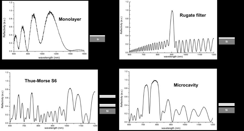
of porous silicon.
which optically act as a Fabry-Perot interferometer, to complex sequences
From homogeneous layers, which optically act as a Fabry-Perot interferometer, to complex sequences of layers having different
thicknesses
of and refractive
layers having different indexes,
thicknesses suchand as Bragg mirrors
refractive or optical
indexes, such microcavities
as Bragg mirrors or Thue-Morse
or optical
sequences, theoroptical
microcavities spectrum
Thue-Morse is not noisy
sequences, the and its evolution
optical spectrum during the experiment
is not noisy and its evolutioncan be used
duringto
quantify
the chemical
experiment can and
bebiological interactions
used to quantify that happen
chemical on PSi surface.
and biological More simply,
interactions that happen especially
on PSiin
time-resolved
surface. measurements,
More simply, especially theinPSi componentsmeasurements,
time-resolved can be read out atPSi
the a single wavelength
components can be byread
usingouta
monochromatic
at source (a
a single wavelength bylaser
using or a LED) and a photodetector.
monochromatic source (a laserRemaining
or a LED)precisely
and on this point, the
a photodetector.
time response
Remaining of an optical
precisely on thisPSi sensor
point, theistimeveryresponse
fast; on the
of an order of microseconds
optical PSi sensor is very [12,13].fast;Asona the
matter of
order
fact,
of changes in the[12,13].
microseconds refractiveAs index
a matter can be of revealed immediately,
fact, changes in the whereas
refractivetheindexelectrical
can counterparts
be revealed
are linked to the
immediately, transit
whereas thetime of the counterparts
electrical charge carriers are[14].
linkedThe toresponse
the transit time
time can
of bethefurther
chargereduced
carriers
whenThe
[14]. the response
optically time
activecanPSibe elements
further are integrated
reduced whenintothe microfluidic
optically active systems that increase
PSi elements their time
are integrated
performances
into by reducing
microfluidic systems that the increase
volume of the time
their sample used [15]. Integrability
performances by reducingand fast response
the volume of thecan also
sample
be ascribed
used to the pros of
[15]. Integrability and PSi.
fast response can also be ascribed to the pros of PSi.Sensors 2019, 19, 4776 4 of 8
Sensors 2019, 19, x FOR PEER REVIEW 4 of 8
Figure Optical
2. 2.
Figure spectra
Optical spectraofofdifferent
differentPSi
PSioptical
optical structures. Hstands
structures. H standsfor
forthe
thehigh
highporosity
porosity layer,
layer, L for
L for
thethe
low porosity
low layer.
porosity layer.The
Thenumbers
numbersindicate
indicatehow
how many pairs
pairs of
ofH-L
H-Llayers
layersconstitute
constituteeach
each structure.
structure.
In In
addition
addition totothe
thetransducer
transducermaterial,
material, thethe other key key issue
issuein inaabiosensor
biosensorisisthethe molecular
molecular probe,
probe,
i.e.,i.e.,
thethenatural
natural(such
(suchasasantibodies,
antibodies,DNADNAfragments,
fragments, proteins, enzymes,and
proteins, enzymes, andsosoon)on)ororsynthetic
synthetic (like
(like
aptamers,
aptamers, PNA,PNA, short
short chains,
chains, andand others)
others) element
element thatthat
hashasthe the
rolerole of selectively
of selectively recognizing
recognizing the
the target
target All
analyte. analyte. Allprobes
of these of these probes or
evolved evolved
have beenor have been designed
designed to work intosolution,
work in rather
solution,
thanrather
when than
fixed
when fixed on a support surface. The functionalization of the transducer
on a support surface. The functionalization of the transducer surface is a crucial point in realizing surface is a crucial point inan
realizing an effective device. There are really a lot of chemical and physical
effective device. There are really a lot of chemical and physical strategies for modifying the surfaces of strategies for modifying
the surfaces
optical devices. of The
optical
twodevices. The twoare
main options main theoptions are the spontaneous
spontaneous absorption of absorption
biomolecularof biomolecular
probes onto
probes onto the transducer surface, which gives a disordered assembly
the transducer surface, which gives a disordered assembly and an incompletely covered support; and an incompletely covered or
support; or the covalent binding of the probes to surface, which is a much
the covalent binding of the probes to surface, which is a much more controlled process. In both the more controlled process.
In both the cases, a thin layer of a few nanometers of biological material that is not densely packed
cases, a thin layer of a few nanometers of biological material that is not densely packed should be
should be carefully analyzed in order to design the biosensor performances. On a planar surface, this
carefully analyzed in order to design the biosensor performances. On a planar surface, this is not
is not simple, and sophisticated techniques such as X-ray photoelectron spectroscopy must be used.
simple, and sophisticated techniques such as X-ray photoelectron spectroscopy must be used. The
The situation is much easier in the case of PSi structures, which always have very large specific
situation is much easier in the case of PSi structures, which always have very large specific surface
surface area that amplifies the effect of the functionalization treatment. From this point of view, a PSi
area that amplifies the effect of the functionalization treatment. From this point of view, a PSi layer is
layer is the perfect support for the development and optimization of a surface functionalization
theprocess
perfect[16].
support for the development
The as-etched PSi surface isand optimization
highly hydrophobic, of adue
surface functionalization
to the processbut
acid-based fabrication, [16].
Theit as-etched
can easily PSi surfaceinto
be turned is highly hydrophobic,
a hydrophilic due toseveral
one through the acid-based
oxidationfabrication,
treatments.but it can easily
Moreover, therebe
turned into a hydrophilic one through several oxidation treatments. Moreover,
is at least one procedure that transforms PSi into an ultra-stable material: thermal acetylation, which there is at least one
procedure that transforms
was discovered PSi into
by J. Salonen at an ultra-stable
University material:
of Turku, thermal
Finland acetylation,
[17]. The tunable which
surfacewaschemistry
discovered
by makes
J. Salonen at University
PSi devices of Turku,
more useful than Finland
those made [17].
in The tunable
planar surface chemistry makes PSi devices
configuration.
more useful than those
In summary, made in planar
a high-quality, fast,configuration.
and specific optical response, a great surface area (up to
In summary,
hundreds a high-quality,
of square meter perfast, anddue
gram) specific
to theoptical
porous response, a greatand
morphology, surface area (up to hundreds
a customizable surface
chemistry
of square metera great flexibility
per gram) due totothe
PSiporous
biosensors for veryand
morphology, different applications
a customizable in environment
surface chemistry a great or
healthcare
flexibility monitoring.
to PSi biosensors for very different applications in environment or healthcare monitoring.
3. The
3. The Cons
Cons ofof PSiTechnology
PSi Technology
After
After listing
listing all all of the
of the advantages
advantages of this
of this material,
material, it is natural
it is natural to wonder
to wonder why itwhy it is
is still still
not not
possible
possible
to find to find
devices devices
based based on
on porous porous
silicon silicon
in the in the pharmacy
pharmacy or amongorconsumer
among consumer
electronicselectronics
products.
products.
Let’s now face Let’s
thenow
mainface the that
issues mainuntil
issues
nowthat until
have now have
prevented theprevented
diffusionthe diffusion of
of PSi-based PSi-based
products onto
products onto the market. The doping level and the hydrogen contamination
the market. The doping level and the hydrogen contamination of crystalline silicon wafers of crystalline silicon
can be
wafers from
different can beonedifferent
pack to from one pack
another, andtoeven
another, andsame
in the evenlot in the same lotso
of wafers, of that
wafers,
theso that fabrication
same the sameSensors 2019, 19, 4776 5 of 8
recipe applied to two different silicon wafers can generate quite different PSi structures. In particular,
hydrogen contamination is responsible for the presence of a top layer, near the wafer surface, with
very small pores (under 5 nm) that prevent the penetration of liquids inside the PSi. This top layer
can be avoided by removing a few microns of silicon by controlled electropolishing before starting
the electrochemical etching of the designed structure. Furthermore, it should be noted that even
if the geometry of the platinum cathode should guarantee a homogeneous dissolution rate of the
entire silicon surface, this does not actually happen. There is always a small difference in the porosity
and thickness values between the edge of the PSi area and its center, and also between the top and
the bottom of the layer [18]. This inhomogeneity is reflected in the optical spectrum, which can be
different when recorded at different points of the device’s surface. From this perspective, a PSi optical
transducer could show different signals from point to point, and, moreover, different spectra from
sample to sample. The large-scale industrial production of PSi-based devices is seriously hampered by
the intrinsic limitation of the fabrication method. Even if all the steps, from the electrochemical etching
to the bioprobe binding, could be individually calibrated, the sum of all of them remains unpredictable,
so that the only way to use a PSi biosensor is to calibrate each single device. This solution could be
economically sustainable only for those applications with a very high added value [19,20].
The freshly etched PSi surface is highly hydrogenated, and since the chemical bond between
silicon and hydrogen (namely, Si-H) is not thermodynamically very stable, it tends to be substituted
by Si-O on exposure to atmospheric oxygen. The silicon oxide has a refractive index value much
lower than crystalline silicon, such that the spontaneous aging of the porous silicon surface strongly
affects the optical spectrum, and also compromises the complex multilayered structures. There are a
lot of procedures for passivating and stabilizing the PSi surface, but the complete chemical stability in
either acid or oxidizing solution is hard to obtain [21]. This is another difficult issue to overcome that
sometimes precludes good repeatability among the results of different experiments obtained using the
same device.
4. Conclusions and Further Perspectives
Three review papers regarding PSi-based optical biosensors have recently been published, and they
give a wide and complete overview of this subject, along with the references reported therein [22–24].
In particular, the paper by N.H. Maniya reports a very interesting summary of the detection of various
biomolecules using PSi optical devices. An extract of that summary is reported in Table 1 for the
purposes of discussion.
Table 1. Examples of detection of different biomolecules using PSi optical biosensors. Adapted from
Ref. [24].
Detection Response
Analyte Probe PSi Device Sensitivity Ref.
Range Time
DNA (15 mer) ssDNA Single layer 1–10 nM 1 nM 20 min [25]
Metallo-proteinase Peptide Microcavity 10−7 –10−12 M 10−19 M 15 min [26]
Subtilisin Gelatin Bloch surface wave 0.01 mg/mL 1.8 pM 20 min [27]
Vancomycin Peptide Double layer 0.005–0.1 mg/mL 0.005 mg/mL 20 min [28]
The performances of PSi-based optical biosensors reported in Table 2 are equivalent to or
exceed those of corresponding devices made of other materials, as reported in the most current
literature [29–31].Sensors 2019, 19, 4776 6 of 8
Table 2. Summary of pros and cons of PSi technology.
Pros Cons
Low costs and simple (but not trivial) fabrication
Intrinsic limitation of the etching process
equipment and procedures
Easy and fast read out Spontaneous aging and chemical instability
Integrated microelectronics compatibility Single device calibration
Tunable morphology, dielectric properties and
surface chemistry
Huge specific surface area
Biocompatibility
Extreme flexibility in different application fields
Despite these results, there is no doubt that the most interesting prospect in the field of technological
applications of PSi, and also that with the greatest marketing possibilities, is not that of devices made
on chips, but rather that of silicon nanostructured powders. Nevertheless, it can be noted that the
advantages of using PSi as a material for the optical transduction of molecular interactions largely
overcome the disadvantages, as is clearly shown in Table 2.
So many good features in a single material greatly justify the success and the diffusion of PSi in
the laboratories focused on optical biosensing that are spread all over the world. The PSi scientific
community is very active and collaborative and often meets at international congresses dedicated to
the science and technology of porous semiconductors.
In conclusion, there are strong indications in the direction of constant attention being directed
towards the development of PSi biosensors by several academic groups in the mid-term, i.e., in the
next five years. The final approach of these products to the commercial market will also depend on a
variety of factors directly connected to economic and financial aspects, which can in future change the
trends and determine the success of industrial initiatives. PSi optical transducers are thus surely not a
failure from a scientific point of view, and they could become successful devices in the near future,
even if more effort needs to be directed towards their development.
Funding: This research received no external funding.
Acknowledgments: The author wishes to acknowledge the ASCOS 2019 organizing committee, in particular F.
Baldini and A. Giannetti from IFAC-CNR, Italy, for the invitation to attend the school teaching board.
Conflicts of Interest: The author declares no conflict of interest.
References
1. Lin, V.S.Y.; Motesharei, K.; Dancil, K.P.S.; Sailor, M.J.; Ghadiri, M.R. A porous silicon-based optical
interferometric biosensor. Science 1997, 278, 840–843. [CrossRef] [PubMed]
2. Sailor, M.J. Porous Silicon in Practice: Preparation, Characterization and Applications, 1st ed.; John Wiley and
sons: Hoboken, NJ, USA, 2012.
3. Michael, J. Sailor Biography. Available online: http://sailorgroup.ucsd.edu/research/movies.html (accessed
on 16 September 2019).
4. Oton, C.J.; Dal Negro, L.; Gaburro, Z.; Pavesi, L.; Johnson, P.J.; Lagendijk, A.; Wiersma, D.S. Light propagation
in one-dimensional porous silicon complex systems. Phys. Status Solidi (a) 2003, 197, 298–302. [CrossRef]
5. Moretti, L.; Rea, I.; Rotiroti, L.; Rendina, I.; Abbate, G.; Marino, A.; De Stefano, L. Photonic band gaps analysis
of Thue-Morse multilayers made of porous silicon. Opt. Express 2006, 14, 6264–6272. [CrossRef] [PubMed]
6. Ligler, F.S.; Taitt, C.R. (Eds.) Optical Biosensors: Today and Tomorrow; Elsevier: Amsterdam, The Netherlands,
2011.
7. Korotcenkov, G. (Ed.) Formation and Properties. In Porous Silicon: From Formation to Application; Taylor and
Fracis Group, CRC Press: Boca Raton, FL, USA, 2015; Volume 1.Sensors 2019, 19, 4776 7 of 8
8. Surdo, S.; Carpignano, F.; Merlo, S.; Barillaro, G. Near-Infrared Silicon Photonic Crystals with High-Order
Photonic Bandgaps for High-Sensitivity Chemical Analysis of Water–Ethanol Mixtures. ACS Sens. 2018, 3,
2223–2231. [CrossRef] [PubMed]
9. Mariani, S.; Robbiano, V.; Strambini, L.M.; Debrassi, A.; Egri, G.; Dähne, L. Layer-by-layer biofunctionalization
of nanostructured porous silicon for high-sensitivity and high-selectivity label-free affinity biosensing. Nat.
Commun. 2018, 9, 5256. [CrossRef]
10. De Stefano, L.; Rotiroti, L.; Rea, I.; Rendina, I.; Moretti, L. Quantitative measurements of hydro-alcoholic
binary mixtures by porous silicon optical microsensors. Phys. Stat. Sol. (c) 2007, 4, 1941–1945. [CrossRef]
11. Moretti, L.; De Stefano, L.; Rea, I.; Rendina, I. Periodic versus aperiodic: Enhancing the sensitivity of porous
silicon based optical sensor. Appl. Phys. Lett. 2007, 90, 191112. [CrossRef]
12. De Stefano, L.; Rendina, I.; Moretti, L.; Rossi, A.M. Time-resolved sensing of chemical species in porous
silicon optical microcavity. Sens. Actuators B 2004, 100, 168–172. [CrossRef]
13. De Stefano, L.; Malecki, K.; Della Corte, F.G.; Moretti, L.; Rotiroti, L.; Rendina, I. Integrated silicon-glass
opto-chemical sensors for lab-on-chip applications. Sens. Actuators B 2006, 114, 625–630. [CrossRef]
14. Korotcenkov, G.; Rusu, E. How to Improve the Performance of Porous Silicon-Based Gas and Vapor Sensors?
Approaches and Achievements. Phys. Status Solidi A 2019. [CrossRef]
15. Rea, I.; Lamberti, A.; Rendina, I.; Coppola, G.; Gioffrè, M.; Iodice, M.; Casalino, M.; De Tommasi, E.; De
Stefano, L. Fabrication and Characterization of a Porous Silicon Based Microarray for Label-free Optical
Monitoring of Biomolecular Interactions. J. Appl. Phys. 2010, 107, 014513. [CrossRef]
16. Rea, I.; Oliviero, G.; Amato, J.; Terracciano, M.; Mayol, L.; Borbone, N.; Piccialli, G.; Rendina, I.; De Stefano, L.
Aminosilane functionalizations of mesoporous oxidized silicon for oligonucleotides synthesis and detection.
J. R. Soc. Interface 2013, 10, 1742–5662.
17. Salonen, J.; Björkqvist, M.; Laine, E.; Niinistö, L. Stabilization of porous silicon surface by thermal
decomposition of acetylene. Appl. Surf. Sci. 2004, 225, 389–394. [CrossRef]
18. Lehmann, V. Electrochemistry of Silicon: Instrumentation, Science, Materials and Applications; Wiley-VCH Verlag
GmbH: Weinheim, Germany, 2002.
19. Canham, L. (Ed.) Handbook of Porous Silicon; Springer: Berlin/Heidelberg, Germany, 2014.
20. Pace, S.; Seantier, B.; Belamie, E.; Lautrédou, N.; Sailor, M.J.; Milhiet, P.E.; Cunin, F. Characterization of
phospholipid bilayer formation on a thin film of porous SiO2 by reflective interferometric Fourier transform
spectroscopy (RIFTS). Langmuir 2012, 28, 6960–6969. [CrossRef] [PubMed]
21. Liu, Z.; Li, Y.; Li, W.; Xiao, C.; Liu, D.; Dong, C.; Hirvonen, J.T.; Zhang, M.; Kemell, M.; Zhang, H.; et al.
Multifunctional nanohybrid based on porous silicon nanoparticles, gold nanoparticles, and acetalated
dextran for liver regeneration and acute liver failure theranostics. Adv. Mat. 2018, 30, 1703393. [CrossRef]
22. Arshavsky-Graham, S.; Massad-Ivanir, N.; Segal, E.; Weiss, S. Porous silicon-based photonic biosensors:
Current status and emerging applications. Anal. Chem. 2018, 91, 441–467. [CrossRef]
23. Terracciano, M.; Rea, I.; Borbone, N.; Moretta, R.; Oliviero, G.; Piccialli, G.; De Stefano, L. Porous Silicon-Based
Aptasensors: The Next Generation of Label-Free Devices for Health Monitoring. Molecules 2018, 24, 2216.
[CrossRef]
24. Maniya, N.H. Recent Advances in Porous Silicon Based Optical Biosensors. Rec. Adv. Mater. Sci. 2018, 53,
49–73. [CrossRef]
25. Vilensky, R.; Bercovici, M.; Segal, E. Oxidized porous silicon nanostructures enabling electrokinetic transport
for enhanced DNA detection. Adv. Funct. Mater. 2015, 25, 6725. [CrossRef]
26. Krismastuti, F.S.; Pace, S.; Voelcker, N.H. Porous silicon resonant microcavity biosensor for matrix
metalloproteinase detection. Adv. Funct. Mater. 2014, 24, 3639. [CrossRef]
27. Qiao, H.; Guan, B.; Gooding, J.J.; Reece, P.J. Protease detection using a porous silicon based Bloch surface
wave optical biosensor. Opt. Express 2010, 18, 15174–15182. [CrossRef] [PubMed]
28. Pacholski, C.; Perelman, L.A.; VanNieuwenhze, M.S.; Sailor, M.J. Small molecule detection by reflective
interferometric Fourier transform spectroscopy (RIFTS). Phys. Status Solidi A 2009, 206, 1318–1321. [CrossRef]
29. Steglich, P.; Hülsemann, M.; Dietzel, B.; Mai, A. Optical biosensors based on silicon-on-insulator ring
resonators: A review. Molecules 2019, 24, 519. [CrossRef] [PubMed]Sensors 2019, 19, 4776 8 of 8
30. Soler, M.; Huertas, C.S.; Lechuga, L.M. Label-free plasmonic biosensors for point-of-care diagnostics: A
review. Expert Rev. Mol. Diagn. 2019, 19, 71–81. [CrossRef]
31. Chen, Y.; Liu, J.; Yang, Z.; Wilkinson, J.S.; Zhou, X. Optical biosensors based on refractometric sensing
schemes: A review. Biosens. Bioelectron. 2019, 144, 111693. [CrossRef]
© 2019 by the author. Licensee MDPI, Basel, Switzerland. This article is an open access
article distributed under the terms and conditions of the Creative Commons Attribution
(CC BY) license (http://creativecommons.org/licenses/by/4.0/).You can also read