Radar baseboard MCU7 - Infineon Technologies
←
→
Page content transcription
If your browser does not render page correctly, please read the page content below
AN599

  Radar baseboard MCU7
  60 GHz radar system platform

  Board version 2.2

  About this document
  Scope and purpose

  This application note describes the radar baseboard MCU7, part of Infineon’s 60 GHz radar system platform. It
  also introduces the concept of the platform which supports multiple sensors. At the heart of the board is the
  Microchip ATSAMS70Q21, a 32-bit ARM Cortex-M7 MCU. The microcontroller enables interfacing up to two
  sensors. It also provides a Hi-Speed USB 2.0 interface to a host computer for visualization or fast data processing.
  In addition, the board is compatible with the Arduino MKR standard, which facilitates access to existing mass-
  market daughter boards for mass data storage or wireless communication Arduino boards.

  Intended audience
  This document is intended for anyone working with Infineon’s 60 GHz radar system platform.

  Application Note         Please read the Important Notice and Warnings at the end of this document
  www.infineon.com                                        page 1 of 23                                      2021-05-30
Radar baseboard MCU7
60 GHz radar system platform
Introduction

Table of contents
About this document ....................................................................................................................... 1
Table of contents ............................................................................................................................ 2
1      Introduction .......................................................................................................................... 3
1.1          60 GHz radar system platform ................................................................................................................ 3
1.2          Board overview and key features ........................................................................................................... 3
2      Sensor interface ..................................................................................................................... 5
2.1         Overview .................................................................................................................................................. 5
2.2         Supply ...................................................................................................................................................... 6
2.3         Level shifters ............................................................................................................................................ 7
2.4         Sensor connectors................................................................................................................................... 8
2.5         Current measurement of radar sensor boards..................................................................................... 10
3      Arduino MKR interface ........................................................................................................... 12
4      Firmware ............................................................................................................................. 13
4.1         USB......................................................................................................................................................... 14
4.2         EEPROM ................................................................................................................................................. 14
4.3         RGB LED ................................................................................................................................................. 15
4.4         Firmware development and debugging ............................................................................................... 16
4.5         Flashing via boot loader ........................................................................................................................ 16
5      Microcontroller pin map......................................................................................................... 17
5.1         Sensor interface 1.................................................................................................................................. 17
5.2         Sensor interface 2.................................................................................................................................. 18
5.3         Arduino MKR interface .......................................................................................................................... 19
5.4         Other pins .............................................................................................................................................. 20
6      References ........................................................................................................................... 21
Revision history............................................................................................................................. 22

Application Note                                                               2 of 23                                                                      2021-05-30
Radar baseboard MCU7
60 GHz radar system platform
Introduction

1                  Introduction
 1.1               60 GHz radar system platform
The 60 GHz radar system platform is the evaluation platform for Infineon’s 60 GHz radar sensors. It consists of
the radar baseboard MCU7 as the microcontroller board and a radar sensor board, e.g. BGT60TR13C shield for
BGT60TR13C. Figure 1 illustrates the radar baseboard MCU7 with a sensor board. Both boards have markers.
These markers must be aligned to plug in the sensor board correctly.

                     a)          Radar baseboard MCU7
                                                                      Markers

                                                                           Sensor board
                                 b)

Figure 1           The 60 GHz radar system platform with a sensor board (a) unplugged or (b) plugged in

 1.2               Board overview and key features
 a)                        Top side                      b)                  Bottom side

Figure 2           The radar baseboard MCU7

The radar baseboard MCU7, illustrated in Figure 2, is a 40.64 mm x 25.4 mm printed circuit board (PCB). Its main
purpose is to provide a generic sensor interface for Infineon’s 60 GHz radar sensors. The central microcontroller
unit (MCU) can perform radar data processing or forward the sensor data to a USB interface or an Arduino MKR
interface. The board’s block diagram is depicted in Figure 3 and its key features are as follows:

Application Note                                     3 of 23                                           2021-05-30
Radar baseboard MCU7
60 GHz radar system platform
Introduction

    •    ARM Cortex-M7 MCU: The central device on the radar baseboard MCU7 is an ATSAMS70Q21, a 32-bit ARM
         Cortex M7 MCU. It runs at a clock frequency of 300 MHz and contains 384 kByte SRAM. The microcontroller
         is supplied with 3.3 V, which is decoupled from the other 3.3 V supplies for the sensors to minimize cross-
         talk between the digital signals and the sensor supply.

    •    USB interface: Since radar data acquisition can generate significant amounts of raw data, a Hi-Speed-
         USB interface with data rates of up to 480 Mbit/s is used on the radar baseboard MCU7. This provides
         sufficient bandwidth to forward all radar data to a host PC for visualization or some other powerful
         computer for radar data processing.

    •    Sensor interface: The radar baseboard MCU7 features two radar sensor interfaces. Each sensor
         daughter card contains an EEPROM connected via an I2C interface. This EEPROM contains a descriptor
         indicating the type of the baseboard and sensor. This is used by the firmware to communicate properly
         with the board. It is even possible to detect a wrongly inserted board (rotated by 180 degrees). To enable
         communication with a radar sensor, the board provides an SPI connection, two ADC channels, a DAC
         channel and 10 GPIO pins.

    •    Arduino MKR connector: As radar data processing may require very different application-specific
         hardware, the radar baseboard MCU7 supports the Arduino MKR interface. This gives access to a wide
         assortment of inexpensive add-on hardware for rapid prototyping, like SD cards for raw data storage,
         wireless communication and so on.
    •    RGB LED: The board has an RGB LED to indicate its status. At start-up of the board, the LED will blink. If
         a radar sensor is detected, the LED will turn green. A detailed description of the LED status codes can be
         found in Section 4.2.

                                                       5V

                        LDO 3.3V                      3.3V
                                        3.3V
                                                                         I²C
                                                                                     interface 1
                                                                                       Sensor
                                                    ARM Cortex M7

                                                                               2
                                                    ATSAMS70Q21

                            5V                                          GPIO
                        Micro-        USB                                      17

                         USB
                                    3.3V
                                                                               I²C
                                                                                                   interface 2

                            5V
                                                                                                     Sensor

                                                                                     2
                        Arduino MKR        GPIO                           GPIO
                                            10                                       17
                         Connector
                                                                               RGB
                                                                    3          LED
Figure 3           Block diagram of the radar baseboard MCU7

Application Note                                       4 of 23                                                   2021-05-30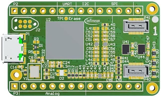
Radar baseboard MCU7
60 GHz radar system platform
Sensor interface

2                  Sensor interface
This section covers the sensor interface that was introduced in the previous section.

 2.1               Overview
                                          5V
                                          Enable
                                                                                                            3.3Vsensor
                                                             LDO
                                                             3.3V
                                                                                                     LDO                             LDO
                                                     3.3Vsensor
                                                                                                     1.8V                            1.5V
                          ARM Cortex M7
                          ATSAMS70Q21

                                                                                      1.8Vsensor
                                                                                                                                       1.5Vsensor

                                          SPI                                         VLS,supply
                                                 4

                                                                                                                 Sensor connectors
                                                                  Level shifter

                                          IRQ                                              SPI
                                                                                                     4
                                                                                        IRQ
                                          RST
                                                                                        RST
                                          GPIO                                          GPIO
                                                 2                                                   2
                                                 Open drain
                                                                                       6
                                           DAC               ADC                           I²C
                                                 1                                2              2
                                                     3.3Vdigital

Figure 4           Block diagram of a sensor interface of the radar baseboard MCU7

The block diagram of a single sensor interface of the radar baseboard MCU7 can be seen in Figure 4. When the
board boots up or when a sensor is plugged into the sensor connectors, the sensor supply is deactivated. During
start-up, only the 3.3 Vdigital (MCU) supply of the EEPROM on the sensor board is active. The MCU detects if a sensor
board is plugged into the connectors. If the sensor board is rotated, the MCU will detect it and signal an error on
the RGB LED – see Section 4.2 for details. If the sensor is plugged in correctly, the MCU will read the information
in the EEPROM. This is how it will get information about what kind of sensor is plugged into the interface. The
power supply of the sensor is only enabled if a correct sensor is detected.
The main communication interface with the sensor is a serial peripheral interface (SPI). Given the discrepancy
between the MCU supply voltage of 3.3 V and the sensor supply voltage of 1.8 V or 1.5 V, a level shifter is employed
to translate between the different voltage levels. The supply voltage of the level shifter is 3.3 V on one side, and
on the second side the power can be supplied from three sources: either directly from the 1.5 V or the 1.8 V supply
or from the sensor connector. If the supply is provided by the sensor connector, the daughter card can provide
its correct level shifter supply voltage from the supplied voltages. Besides the four SPI signals, four more digital
signals are translated:

    •    A hardware reset signal to the sensor

    •    An interrupt signal from the sensor to the MCU to indicate that some action by the MCU is required
    •    Two general purpose input output (GPIO) pins – see Section 2.3 for details

Application Note                                                                  5 of 23                                                           2021-05-30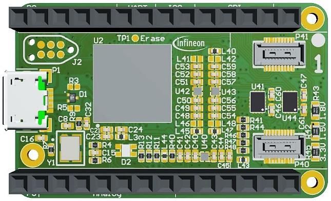
Radar baseboard MCU7
60 GHz radar system platform
Sensor interface

In addition the translated signals the connector also provides:

     •    Two ADC channels
     •    One DAC channel

     •    Six open-drain output signals. One of these is intended to control an LED on the sensor board. The MCU
          will activate the LED by pulling the signal to a low level and deactivate the LED by putting the signal into
          High-Z mode.

    2.2            Supply
                   a)                          5Vusb                        5Vdigital                                        5VSensor1

                                                         L2                                L1

                                                       Ferrite                            10µH
                                         C5                        C6        C7                        C1           C2      C3        C4
                                      100nF            Bead        100nF     10µF                      10µF         10µF    10µF      10µF

                                                                                              fc,low-pass < 8kHz
                   b)
                                                                          en_LDO_1
                                                          en_LDO_1                               NCP163AMX330TBG                                 3V3Sensor1
                                    L43
                    5VSensor1                                                                     IN          OUT
                                Ferrite Bead                                                           EPAD
                                                       C40         C41         C42                EN          GND                  C43       C44       C45
                                                       10µF        10µF        100nF                           U40                 100nF     10µF      10µF
                                    L44
                   3V3Sensor1
                                                  GND            GND       GND                                              GND            GND      GND
                                Ferrite Bead
                                                                                                                      GND
                                    L45                                                          NCP163AMX150TBG                                 1V5Sensor1
                    5VSensor1                                                                     IN          OUT
                                                                                                       EPAD

                                   DNP
                                                       C48         C49         C50                EN          GND                  C51       C52       C53
                                                       10µF        10µF        100nF                           U42                 100nF     10µF      10µF
                                    L46
                   3V3Sensor1
                                                  GND            GND       GND                                              GND            GND      GND
                                Ferrite Bead                                                                          GND
                                    L47                                                          NCP163AMX180TBG                                 1V8Sensor1
                    5VSensor1                                                                     IN          OUT
                                                                                                       EPAD

                                   DNP
                                                       C54         C55         C56
                                                                                                  EN          GND                  C57       C58       C59
                                                       10µF        10µF        100nF       R40                 U43                 100nF     10µF      10µF
                                                                                           10kΩ
                                                  GND            GND       GND                                              GND            GND      GND
                                                                                                                      GND
                                                                                        GND

Figure 5           Sensor supply circuit schematics of sensor 1

Because radar sensors are very sensitive to voltage fluctuations on the supply, a low-noise power supply is vital.
This subsection discusses the supply circuit on the radar baseboard MCU7. Figure 5a depicts the initial stage of
the supply’s circuit. In order to block high-frequency (HF) noise entering the circuit via the USB supply a low-pass
filter has been integrated. This filter consists of the ferrite bead L2 and the capacitors C6 and C7. The filtered
voltage is used to supply the MCU (through a 3.3 V LDO). The MCU operation may cause additional unwanted
voltage fluctuations on the supply.1 Therfore, another low-pass filter is placed in the supply. The filter consists of
the coil L1 and the capacitors C1, C2, C3 and C4, which results in a cut-off frequency below 8 kHz.2 This yields a
stable supply voltage with very low noise inside a frequency range from about 10 kHz up to the MHz regime.
Figure 5b shows the additional supply circuitry that is required for each sensor. The one depicted in Figure 5b is
for sensor 1.3 A ferrite bead is placed at the input side of the supply to block any HF noise from upstream (such
as might be caused by the MCU). This is fed into an LDO to generate an intermediate voltage of 3.3 V for the sensor
supply. This intermediate voltage is further down-converted to 1.8 V and 1.5 V. The LDOs used for power

1
  For example, a PWM signal generated by the MCU would cause noise on the supply at the frequency of the PWM signal and its
    harmonics.
2
  Additional capacitors on the supply line reduce the cut-off frequency even more.
3
  The circuit for sensor 2 is a copy of the circuit of sensor 1.

Application Note                                                                        6 of 23                                                               2021-05-30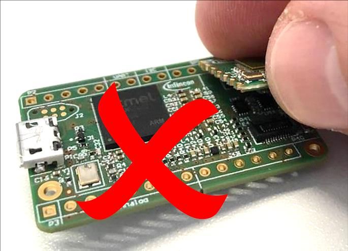
Radar baseboard MCU7
60 GHz radar system platform
Sensor interface

conversion are ON Semiconductor’s NCP163 low-noise LDOs with an output noise of 6.5 µVRMS. They provide a
power supply rejection ratio above 90 dB. The remaining noise in the system is mainly caused by the LDOs and
tends to be strongest at frequencies around 100 kHz where the LDOs stop working efficiently.
If ghost targets appear in the radar signal, it may be possible to improve the performance by optimizing the
power supply. On the radar baseboard MCU7, the supply of the 1.8 V and 1.5 V LDOs can be changed from 3.3 V
to 5 V by swapping L44 with L45 and L46 with L47. This will affect the noise performance on the 1.5 V supply and
the 1.8 V supply. If L44 and L46 are used, 1.5 V and 1.8 V are each generated with two LDOs in series.1 This
configuration suppresses external low frequency better than a single LDO.
The other option is to directly convert 5 V down to 1.5 V and 1.8 V by using L45 and L47 instead of L44 and L46.
Each LDO generates noise at its maximum suppression frequency, which is typically around 100 kHz. This
frequency is in the frequency range of the radar IF signals. Hence, noise in that this frequency range can cause
ghost targets in radar data processing. In the configuration with two LDOs in series (L44 and L46), the noise
caused by the first LDO stage will be amplified by the second stage. To minimize the noise around 100 kHz, a
single LDO stage can be used in the configuration with L45 and L47. To summarize, for supplies with strong low-
frequency noise components, it is better use L44 and L46, while for low-noise supplies L45 and L47 are preferable.

    2.3             Level shifters
This subsection explains the level shifter circuit on the radar baseboard MCU7.
                                                                                       1V5Sensor1     1V8Sensor1 3V3Sensor1
                                                                          Vdigital_1

                                                                                                                          Ferrite Bead
                                                                                L40        L41        L42           L43
                                                                        Ferrite Bead       DNP        DNP
                                                        U41
                                R41   S1_SPI_OEn                                                    VCCA1
                       GND                               1OE_N     VCCA
                               10kΩ                                                                 VCCB1
                                                        2OE_N      VCCB
                       VCCA1    R44   S1_SPI_DIR             0
                                                        1DIR 1         GND                                  C46           C47
                               10kΩ                                                                         100nF         100nF
                                                        2DIR 01        GND
                                                                                                                    GND
                                      S1_SPI_CLK                                 SPI_CLK_1
                                                        1A1            1B1
                                      S1_SPI_MOSI                                SPI_MOSI_1
                                                        1A2            1B2
                                      S1_RST                                     BGT_RST_1
                                                        2A1            2B1
                                      S1_SPI_CSN                                 SPI_CSN_1
                                                        2A2            2B2
                                                        SN74AVC4T245RSVR

                                                        U44
                                      S1_SPI_OEn                                 VCCA1 C60
                                                        1OE_N      VCCA                                     GND
                                R46                                                              100nF
                       VCCA1          S1_GPIO_OEn                                VCCB1 C61
                                                        2OE_N      VCCB                                     GND
                                    10kΩ                                                         100nF
                                R47   S1_SPI_READ_DIR        0
                       GND                              1DIR 1         GND
                                    10kΩ
                       VCCA1    R48   S1_GPIO_DIR            0
                                                        2DIR 1         GND         GND
                                    10kΩ

                                      S1_SPI_MISO                                SPI_MISO_1
                                                        1A1            1B1
                                      S1_IRQ                                     BGT_IRQ_1
                                                        1A2            1B2
                                      S1_GPIO1                                   GPIO1_1
                                                        2A1            2B1
                                      S1_GPIO2                                   GPIO2_1
                                                        2A2            2B2
                                                        SN74AVC4T245RSVR

Figure 6             Level shifter circuit of sensor 1

1
    U40 and U42 generate 1.5 V. U40 and U43 create the 1.8 V domain.

Application Note                                                  7 of 23                                                                2021-05-30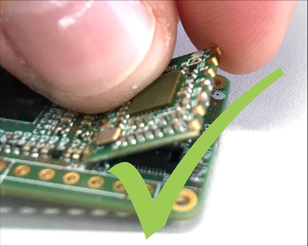
Radar baseboard MCU7
60 GHz radar system platform
Sensor interface
Figure 6 illustrates the level shifter circuit for sensor 1. The circuit for sensor 2 is equal to the one for sensor 1
except for the other signal lines that are used for sensor 2. The level shifters can either be powered by one of the
sensor supplies or with a voltage from the sensor interface. With this voltage from the sensor interface, the
daughter card has the option to choose its preferred supply voltage. To minimize interference from digital signals
on the supply voltage, the level shifters are decoupled from the sensor supplies. This is done by using ferrite
beads with high suppression in the MHz regime.
Pull-up and pull-down resistors are connected to the enable and direction pins. This provides a pre-set so that
SPI level translation is enabled with the direction configured so that the MCU is the master and the sensor is the
slave. If a different configuration is required, the MCU can directly drive those pins. See Table 5 and Table 6 for
details.
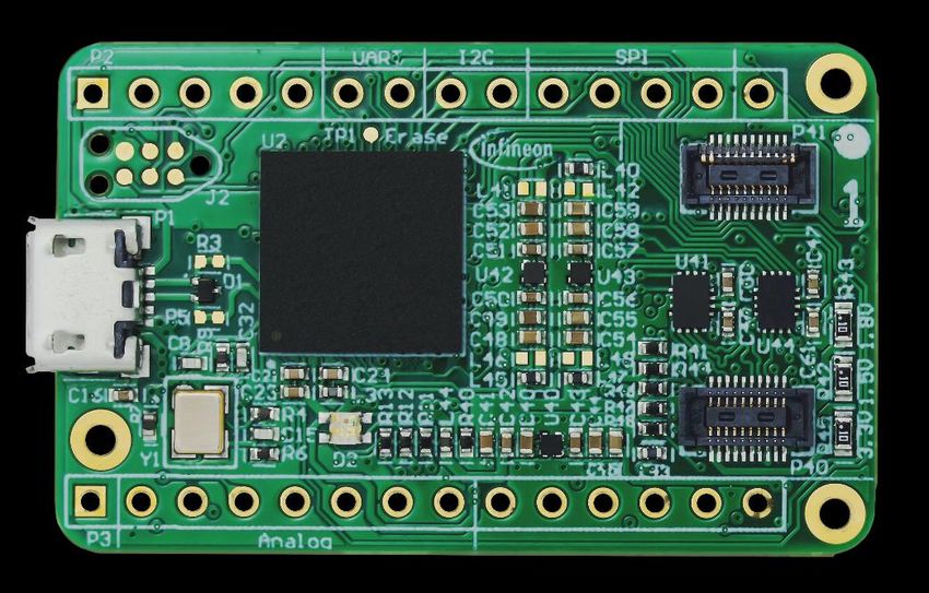
2.4 Sensor connectors
Top side Sensor interfaces Bottom side
LDO for sensor interface supply
Figure 7 Sensor interfaces on the radar baseboard MCU7
As illustrated in Figure 7, the board features two sensor interfaces. The one on the top side of the PCB is labeled
“1” and the one on the bottom side of the PCB is labeled “2”. Next to the label, a white filled circle is drawn as a
marker. A complementary marker is to be found on the sensor board – see Figure 1. For correct mounting of a
sensor, the markers of the radar baseboard MCU7 and the sensor board have to be aligned.
a) b)
Figure 8 How to unplug the sensor-to-sensor connectors of the radar baseboard MCU7
Hirose’s DF40C-20DS-0.4V connectors are used for the sensor interfaces on the radar baseboard MCU7. On the
sensor board matching DF40C-20DP-0.4V connectors are used. There is a risk of the connectors wearing out when
Application Note 8 of 23 2021-05-30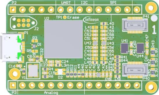
Radar baseboard MCU7
60 GHz radar system platform
Sensor interface

regularly plugged into and unplugged from the sensor. To prevent this, do not lift the sensor on the short side
out of the connector, as illustrated in Figure 8a. Instead simply pull on the long side of the sensor, thereby tilting
the short side, as shown in Figure 8b. This will significantly increase the lifetime of the connectors.

     a)   3V3digital
                                     1
                                         P40
                                                   2
                                                                     GND
                                                                                       OpenDrain_LED_1 1
                                                                                                           P41
                                                                                                                     2
                        I2C_SDA_1    3             4    I2C_SCL_1                      DAC_1           3             4
                                     5             6    BGT_IRQ_1                      ADC2_1          5             6
               GND                   7             8                                   ADC1_1          7             8
                                                        SPI_CLK_1
                          R42        9             10   SPI_MOSI_1                     GPIO2_1         9             10
      1V5Sensor1                    11             12   SPI_MISO_1                     Vdigital_1    11              12
                   0.1R 1%
                          R43       13             14   GPIO1_1                        OpenDrain4_1 13               14
      1V8Sensor1                    15             16
                          0.1R 1%                       BGT_RST_1                      OpenDrain3_1 15               16
                                                                                                                                     GND
                                    17             18   SPI_CSN_1                      OpenDrain1_1 17               18 OpenDrain2_1
                          R45       19             20                                                 19             20
      3V3Sensor1                                                                 GND                                                3V3digital
                   0.1R 1%
                                         DF40C-20DS-0.4V(51)                                               DF40C-20DS-0.4V(51)

     b)

            3V3Sensor1                                                                              GND                              3V3digital
            3V3Sensor1                                  SPI_CSN_1                          OpenDrain1_1                              OpenDrain2_1
            1V8Sensor1                                  BGT_RST_1                          OpenDrain3_1                              GND
            1V8Sensor1                                  GPIO1_1                            OpenDrain4_1
            1V8Sensor1                                  SPI_MISO_1                            Vdigital_1
            1V5Sensor1                                  SPI_MOSI_1                              GPIO2_1
            1V5Sensor1                                  SPI_CLK_1                                ADC1_1
                   GND                                  BGT_IRQ_1                                ADC2_1
             I2C_SDA_1                                  I2C_SCL_1                                 DAC_1
              3V3digital                                GND                             OpenDrain_LED_1

                                                                       12mm
Figure 9               Schematics (a) and pad layout (b) of the connectors for sensor 1.

Figure 9 depicts the schematics (a) and the pad layout (b) of the connectors for sensor 1. Since it is possible to
plug the same sensor into either interface, the schematics and pad layout for both are equal except for the
different signal names for sensor 2. The two connectors of a sensor interface are separated by 12 mm and Figure
9 also illustrates the silkscreen marking for the correct alignment of a sensor with one of the radar baseboard
MCU7’s sensor interface.
If a sensor is plugged in incorrectly (rotated by 180 degrees), GND and 3V3digital will still be matched between
the MCU board and sensor board. Therefore, the sensor’s I2C signal lines for the EEPROM will still be pulled up
and the MCU will notice that OpenDrain1_1 and OpenDrain2_1 are pulled up instead of its I2C signals. This is how
the MCU can detect that the sensor is plugged in correctly (I2C signals pulled up) or incorrectly (OpenDrain1_1
and OpenDrain2_2 pulled up).
The main sensor interface is full duplex SPI. Besides the eight level-shifted signals that were explained in Section
2.3, one line provides a possible supply source for the level shifters, which allows the daughter cards to set their
digital voltage level. Besides these signals, there are three analog lines connected to the MCU, two ADC channels
and a DAC channel, which can be used on the sensor board. Furthermore, there are five digital signals connected,
which can only be used in open-drain mode because they are not level shifted.

Application Note                                                       9 of 23                                                               2021-05-30
Radar baseboard MCU7
60 GHz radar system platform
Sensor interface

    2.5              Current measurement of radar sensor boards
                Top side                                  Bottom side

                                                                                                             Shunt resistors
Figure 10             Shunt resistors of the radar baseboard MCU7 for current measurement of the radar sensor
                      boards

When radar sensors are used in mobile applications, the power consumption must be minimized to improve
battery lifetime. The radar GUI provides an estimate of the expected average power consumption for the
configured settings. If a measurement of the actual operating current consumption of the sensor is required,
shunt resistors are provided on the radar baseboard MCU7. The shunt resistors are in series to the supplies of the
two sensors, as illustrated in Figure 10. There is a label next to each shunt resistor to indicate which supply is
measured – see Table 1 for details. All shunt resistors have a resistance of 0.1 Ω. By measuring the voltage drop
along the shunt resistor,1 the user can infer the current supplied to the sensor and multiply it by the voltage
supplied to measure the power consumption of the sensor board. In this way, it is possible to measure the power
supplied on the 1.5 V, the 1.8 V and the 3.3 V supply of the sensor.

Table 1              Shunt resistors and the supplies to which they are attached
          Shunt resistor                    Resistor value                     Sensor interface                                Supply
                R42                        0.1 Ω (1 percent)                          1                                        1.5 V
                R43                        0.1 Ω (1 percent)                          1                                        1.8 V
                R45                        0.1 Ω (1 percent)                          1                                        3.3 V
                R50                        0.1 Ω (1 percent)                          2                                        1.5 V
                R51                        0.1 Ω (1 percent)                          2                                        1.8 V
                R52                        0.1 Ω (1 percent)                          2                                        3.3 V

When measuring the current with an oscilloscope, as illustrated in Figure 11a, two oscilloscope channels are
required. Such a set-up is required for a differential measurement with shared ground. The voltage of interest is
the voltage at channel 1 minus the voltage at channel 2. Figure 11b depicts a typical measurement result during
a chirp of a radar frame. When the RF part of the chip is activated and the PLL starts to lock the frequency, the
current into the BGT60TR13C shoots up. After an overshoot, it decreases before the power amplifier and the ADC
are activated. Then, another current increase can be observed. After the frequency ramp, the required current
drops and a current undershoot can be observed. Due to this resulting oscillation of the charges between buffer
capactors, it is recommended to put the radar sensor in a defined state and let the voltages on the sensor settle.

1
    Make sure to measure the voltage drop along the shunt resistors either differential or potential free.

Application Note                                                    10 of 23                                                            2021-05-30
Radar baseboard MCU7
60 GHz radar system platform
Sensor interface
The resulting constant current can easily be measured with an oscilloscope or a voltmeter by dividing the
measured voltage with the shunt resistance. To compute the power consumption, one has to measure the
current (and thus power) for all states of a radar frame. The next computation step is to calculate the energy
consumed in each state by multiplying the power with the duration. Then, one has to add up all energies of a
frame up to obtain the energy of the whole frame. To get the average power consumption, one has to divide the
energy of the frame with the length of the frame.
a) Rshunt
0.1Ω Ch2 Ch1
VLDO,out VSensor,in
b)
63
f (GHz)
58
PLL Lock
Chirp
Phase
250
200
150
I1V8 (mA)
100
50
0
-50
-100
0 0.05 0.1 0.15 0.2 0.25 0.3 0.35 0.4 0.45
t (ms)
Figure 11 Current measurement with the shunt resistors. The measurement set-up is shown in (a)
and typically measurement results for a single chirp are depicted in (b).
Application Note 11 of 23 2021-05-30Radar baseboard MCU7
60 GHz radar system platform
Arduino MKR interface
3 Arduino MKR interface
The Arduino MKR family is a new Arduino family of boards with a standardized interface that can be used for rapid
prototyping. This new board family contains (among others) the following boards, which can be used as daughter
cards:
• MKR Zero: a board with an SD card slot which enables raw data storage on an SD card
• MKR1000: a board with a WiFi-module for wireless data transfer
• MKR Vidor 4000: a board with an FPGA for parallel data processing and SDRAM for a RAM extension
• MKR2UNO adapter: an adapter board that gives access to the standard Arduino environment with a huge
number of daughter cards
• and many more; a quick Google search for “Arduino MKR boards overview” can provide a good overview.
Top side Bottom side
Arduino MKR connectors
Figure 12 Arduino MKR connector on the radar baseboard MCU7
Besides a 5 V supply, a 3.3 V supply and a voltage reference, the Arduino MKR interface contains both an analog
and a digital interface. The analog interface features seven analog channels. The digital interface is composed of
a UART interface, an SPI interface and seven GPIO pins – see Table 7 for details. Figure 12 shows the Arduino MKR
connectors on the radar baseboard MCU7. On the top side of the PCB, containing the MCU, two female 14-pin
headers can be soldered to the board. On the bottom side of the PCB, two male 14-pin headers can be soldered
to the board. If a sensor is monted on the same side as the Arduino MKR connectors, the connectors might
influence the radar antennas. For this reason, it is recommended to only solder Arduino MKR headers on one side
of the radar baseboard and to plug the radar sensor into the other side of the baseboard.
Application Note 12 of 23 2021-05-30Radar baseboard MCU7
60 GHz radar system platform
Firmware
4 Firmware
The radar baseboard MCU7 comes with a default firmware that is intented to serve as a bridge between a host
(typically a PC) and the sensor shields, which are mounted on the sensor connectors. For this, the firmware
implements logic to:
• communicate with the host via USB
• read and write sensor registers
• read sensor data via SPI
• check if a sensor board is plugged into one of the connectors
• read and write the EEPROM on the sensor board (for example, to identify the board)
• control some auxiliary peripherals such as status LEDs on the baseboard and sensorboard.
In its current state, the firmware does not implement any signal processing. It can receive messages from the
host telling it how to configure the sensor and it can forward acquired data from the sensor to the host. However,
if signal processing is required, this functionality can be added as the MCU is powerful enough. The firmware is
written in a way to minimize the effort of porting it to other microcontrollers. Therefore, the firmware is
structured into the following layers.
• Hardware abstraction layer (HAL): This is the lowest layer and implements all the MCU-specific logic,
such as how to interface with SPI, GPIOs, timers and other HW blocks. When porting to a different MCU,
this layer should be the only one affected. It also implements a USB CDC serial interface that is used by
the communication layer to connect to a host device.
• Driver layer: This layer sits on top of the hardware layer. It provides functions to parameterize and read
data from the sensor. It creates appropriate SPI packets to apply those parameters to the sensor and
calls the SPI functions from the HAL to initiate the data transfer. Furthermore, it decodes SPI data packets
from the sensor received by the HAL. Thereby, the sensor measurements are extracted and passed on to
the layer above. The driver layer is independent of the MCU. However, it is specific to the sensor and
needs to be adapted for every supported sensor.
• Communication layer: This layer sits on top of the driver layer and the hardware layer. It receives
request or command messages from the host via the USB interface. These messages are decoded and
the contained data is extracted. This is done by calling the corresponding functions of the driver layer.
When those functions return with a result, a response message with the result is forwarded to the host.
Messages to the host are also generated on receipt of sensor data from the driver layer. This layer is
hardware independent, too. It uses the HAL USB CDC interface for data transmission to the host.
• Actual firmware: This sits on top of all other layers. The firmware calls the initialization functions of all
lower layers at start-up for configuration of things like SPI speed and GPIO directions. Once the start-up
phase has completed an endless loop is entered, inside which the communication layer is called to fetch
and transmit messages to and from the host.
When integrating a sensor in a custom project without the radar baseboard MCU7 serving as an intermediary, the
following steps will need to be taken in the firmware:
• The hardware abstraction layer needs to be ported to the MCU or application processor used in the
project.
• The driver layer can be taken as is without any modifications.
• The communication layer will not be needed; instead the algorithm can be put at this level.
Application Note 13 of 23 2021-05-30Radar baseboard MCU7
60 GHz radar system platform
Firmware
• The radar baseboard MCU7’s firmware code will not be used; however, the initialization code should be
moved into the MCU of the project.
When porting the whole firmware to a different MCU, it should be sufficient to port the HAL to that MCU.
When adding an algorithm to the firmware, this should be put above the driver layer. Depending on the
requirements, the algorithm can replace the communication layer or be operated in parallel to it.
4.1 USB
The firmware implements a communication device class (CDC) device on the USB interface. That means the USB
interface works like a serial port implementing a bi-directional interface transmitting a stream of bytes in both
directions.
On top of this serial data stream, a message-based protocol is implemented by putting start and end markers
around each message. The first byte of the message specifies the target module of the firmware for which the
message is intended. Bytes 2 and 3 of the message set the length of the message. That way the protocol decoder
knows the length of the message. In conjunction with the start and end markers, it is able to split the received
stream into its constituent packets. The firmware source code includes a part of the communication library that
can be integrated into a host application and provides functions to create and decode the firmware messages.
4.2 EEPROM
The firmware utilizes the EEPROM to detect the shield type. The structure of the EEPROM is given in Table 2. It
also contains a 128-bit board identifier, which can be used to distinguish different boards of the same type. In
addition to that the firmware provides commands to the host to store and retrieve key/value pairs of a limited
size in the EEPROM. The host is free to assign any meaning it wants to those pairs (e.g. the value for a specific key
might refer to radar configuration data while the value for another key might be used to store display settings).
The functions for accessing the EEPROM are part of the communication library that is delivered with the
firmware.
Table 2 System status indication with the RGB LED
Structure Field Description
EEPROM header Header to identify board and EEPROM
Magic 8-byte identifier used to detect if the EEPROM has been initialized
Version 2-byte version number identifying the structure
BoardType Board type identifier which the firmware uses to detect the kind of
board
NvmType Identifier of the EEPROM type. Used by the firmware to distinguish
between different I2C EEPROM configurations (size, page size).
Reserved Reserved space, set to 0
UUID 128-bit UUID that can be used to identify the board.
Directory Table mapping 32-bit keys to data specified at a specific offset in the flash
Entry 1: Key 32-bit key for the first entry
Entry 1: Length of data for the first entry
Length
Entry 1: Page Address of the data for the first entry specified as a page number
Application Note 14 of 23 2021-05-30Radar baseboard MCU7
60 GHz radar system platform
Firmware
… Further entries
Entry N: Key 32-bit key for the Nth entry
Entry N: Length of data for Nth entry
Length
Entry N: Page Address of the data for the Nth entry specified as a page number
Data area The rest of the EEPROM is used to store the data corresponding to the entries in the
directory
Data 1 Data for entry 1 at the page given in the corresponding directory
entry
… Data for further entries
Data N Data for entry N at the page given in the corresponding directory
entry
4.3 RGB LED
The current status of the board is indicated using the RGB LED. After startup of the board and while the board is
idle, the board status is indicated as shown in Table 3. While active, the board status is indicated as shown in
Table 4.
Table 3 Board status after startup and while idle as indicated by the RGB LED.
Blinking pattern
Duration 1 and Duration 2 Duration 3 Duration 4
Board status
color 1 and color 2 and color 3 and color 4
No error detected Long green Long off
No RF board detected Short green Short red
Wrong orientation of sensor board Short red Short off
Unknown sensor board Short yellow Short red
Initialization of senor board failed Short yellow Short red Long yellow Long red
Initialization of I2C subsystem failed Short red Short off Long yellow Long off
Internal error Short yellow Short off Long red Long off
Table 4 Board status while active as indicated by the RGB LED.
Blinking pattern
Duration 1 and Duration 2 Duration 3 Duration 4
System status
color 1 and color 2 and color 3 and color 4
Board is idle Long green Long off
Reading data from SPI Red
Sending data to host Blue
Application Note 15 of 23 2021-05-30Radar baseboard MCU7
60 GHz radar system platform
Firmware
4.4 Firmware development and debugging
The firmware is delivered as a project for the Atmel Studio 7 IDE. Hence compiling, flashing and debugging work
out of the box by simply pressing the corresponding buttons in the IDE. For further details refer to (Microchip,
Atmel Studio 7 User Guide, 2019).
Top side Bottom side
Tag Connect debugger Erase pin Standard debugger
Figure 13 Debug connectors on the radar baseboard MCU7
If the user requires a debugger connector, the board features two options, as illustrated in Figure 13. On the top
side of the radar baseboard MCU7, there is the layout for a Tag Connect debugger. If the user does not want to
buy a Tag Connect debug cable, they can solder a normal 10-pin ARM debugging connector to the pads of
component J1 on the bottom side of the radar baseboard MCU7.
When using a debugger connector the firmware can be programmed directly from Atmel Studio 7 using an Atmel-
ICE programmer or compatible tools (for details see the documentation provided with Atmel Studio).
4.5 Flashing via boot loader
The microcontroller contains a boot loader. This enables firmware updates via the USB interface if a debugger is
not available. Since the device normally boots directly into the firmware without going into the boot loader the
boot loader must be manually activated at first. This can be done by performing the following sequence:
• Disconnect the device from USB.
• Hold the MCU ERASE pin to high by connecting TP1 to 3.3 V (see Figure 13).
• Connect the device to USB again while holding TP1 high.
• Release the ERASE pin (TP1).
• The device is now in boot loader mode.
Once the device is in boot loader mode, the firmware can be programmed using the SAM-BA GUI available for
download from Microchip at (Microchip, SAM-BA Boot Assistant, 2019).
Application Note 16 of 23 2021-05-30Radar baseboard MCU7
60 GHz radar system platform
Microcontroller pin map
5 Microcontroller pin map
5.1 Sensor interface 1
Table 5 Microcontroller pin map of sensor interface 1
Signal name(s) Signal group MCU pin Description
I2C_SCL_1 IC
2
PD28 Clock pin of I2C interface for the EEPROM
I2C_SDA_1 I2C PD27 Data pin of I2C interface for the EEPROM
S1_SPI_CSN
SPI PA11 Chip select pin of SPI sensor interface
SPI_CSN_1
S1_SPI_MISO
SPI PA12 Master Input Slave Output pin of SPI sensor interface
SPI_MISO_1
S1_SPI_MOSI
SPI PA13 Master Output Slave Input pin of SPI sensor interface
SPI_MOSI_1
S1_SPI_CLK
SPI PA14 Clock pin of SPI sensor interface
SPI_CLK_1
S1_RST
GPIO PA0 Level shifted GPIO, used for hardware reset of sensor
BGT_RST_1
S1_IRQ
GPIO PC6 Level shifted GPIO, used for interrupt request of sensor
BGT_IRQ_1
S1_GPIO1
GPIO PA9 Level shifted GPIO, no special purpose
GPIO1_1
S1_GPIO2
GPIO PA10 Level shifted GPIO, no special purpose
GPIO2_1
ADC1_1 Analog PE5 ADC channel 1, analog front end 0 of the MCU
ADC2_1 Analog PC15 ADC channel 2, analog front end 1 of the MCU
DAC_1 Analog PB13 DAC channel, DAC0 of MCU
OpenDrain1_1 Open drain PD16 Not level shifted GPIO, either 3.3 V push-pull or open drain
OpenDrain2_1 Open drain PC9 Not level shifted GPIO, either 3.3 V push-pull or open drain
OpenDrain3_1 Open drain PC28 Not level shifted GPIO, either 3.3 V push-pull or open drain
OpenDrain4_1 Open drain PA27 Not level shifted GPIO, either 3.3 V push-pull or open drain
OpenDrain5_1 Open drain PC8 Not level shifted GPIO, either 3.3 V push-pull or open drain
OpenDrain_LED_1 Open drain PC1 Not level shifted GPIO, either 3.3 V push-pull or open drain
Disable pin of the level shifter for SPI communication – with
S1_SPI_OE Level shifter PD24
external pull-down resistor (high: disable, low: enable)
Direction pin of the level shifter for SPI communication – with
S1_SPI_DIR Level shifter PD11 external pull-up resistor
(high: MCU → sensor, low: sensor → MCU)
Direction pin of the level shifter for SPI communication (MISO) –
S1_SPI_READ_DIR Level shifter PD17 with external pull-down resistor
(high: MCU → sensor, low: sensor → MCU)
Enable pin of the level shifter for GPIO 1 and GPIO2 – with external
S1_GPIO_OE Level shifter PD14
pull-up resistor (high: disable, low: enable)
Direction pin of the level shifter for GPIO 1 and GPIO2 – with
S1_GPIO_DIR Level shifter PD18 external pull-up resistor
(high: MCU → sensor, low: sensor → MCU)
Application Note 17 of 23 2021-05-30Radar baseboard MCU7
60 GHz radar system platform
Microcontroller pin map
5.2 Sensor interface 2
Table 6 Microcontroller pin map of sensor interface 2
Signal name(s) Signal group MCU pin Description
Clock pin of I2C interface for the EEPROM – shared with Arduino
I2C_SCL_2 I2C PA4
MKR interface
Data pin of I2C interface for the EEPROM – shared with Arduino MKR
I2C_SDA_2 I2C PA3
interface
S2_SPI_CLK
SPI PC25 Chip select pin of SPI sensor interface
SPI_CSN_2
S2_SPI_MISO
SPI PC26 Master Input Slave Output pin of SPI sensor interface
SPI_MISO_2
S2_SPI_MOSI
SPI PC27 Master Output Slave Input pin of SPI sensor interface
SPI_MOSI_2
S2_SPI_CLK
SPI PC24 Clock pin of SPI sensor interface
SPI_CLK_2
S2_RST
GPIO PA17 Level shifted GPIO – used for hardware reset of sensor
BGT_RST_2
S2_IRQ
GPIO PC11 Level shifted GPIO – used for interrupt request of sensor
BGT_IRQ_2
S2_GPIO1
GPIO PA7 Level shifted GPIO, no special purpose
GPIO1_2
S2_GPIO2
GPIO PA2 Level shifted GPIO, no special purpose
GPIO2_2
ADC1_2 Analog PD30 ADC channel 1, analog front end 0 of the MCU
ADC2_2 Analog PC13 ADC channel 2, analog front end 1 of the MCU
DAC_2 Analog PD0 DAC channel, DAC1 of MCU
OpenDrain1_2 Open drain PA22 Not level shifted GPIO, either 3.3 V push-pull or open drain
OpenDrain2_2 Open drain PD10 Not level shifted GPIO, either 3.3 V push-pull or open drain
OpenDrain3_2 Open drain PC29 Not level shifted GPIO, either 3.3 V push-pull or open drain
OpenDrain4_2 Open drain PD15 Not level shifted GPIO, either 3.3 V push-pull or open drain
OpenDrain5_2 Open drain PC17 Not level shifted GPIO, either 3.3 V push-pull or open drain
OpenDrain_LED_2 Open drain PC2 Not level shifted GPIO, either 3.3 V push-pull or open drain
Disable pin of the level shifter for SPI communication – with
S2_SPI_OE Level shifter PC3
external pull-down resistor (high: disable, low: enable)
Direction pin of the level shifter for SPI communication – with
S2_SPI_DIR Level shifter PA8 external pull-up resistor
(high: MCU → sensor, low: sensor → MCU)
Direction pin of the level shifter for SPI communication (MISO) –
S2_SPI_READ_DIR Level shifter PD29 with external pull-down resistor
(high: MCU → sensor, low: sensor → MCU)
Enable pin of the level shifter for GPIO 1 and GPIO2 – with external
S2_GPIO_OE Level shifter PA1
pull-up resistor (high: disable, low: enable)
Direction pin of the level shifter for GPIO 1 and GPIO2 – with
S2_GPIO_DIR Level shifter PC10 external pull-up resistor
(high: MCU → sensor, low: sensor → MCU)
Application Note 18 of 23 2021-05-30Radar baseboard MCU7
60 GHz radar system platform
Microcontroller pin map
5.3 Arduino MKR interface
Table 7 Microcontroller pin map of the Arduino MKR interface
Connector Signal name MCU pin Description
P2.1 5Vusb – External 5 V supply
P2.2 –
P2.3 3V3digital VDDIO External 3.3 V supply
P2.4 GND – Ground line
NRST Inverted hardware reset pin of the MCU – with external pull-
P2.5 N_RST
up resistor
P2.6 UART_TX PD26 GPIO, MCU’s UART Tx-pin
P2.7 UART_RX PD25 GPIO, MCU’s UART Rx-pin
GPIO, clock pin of I2C interface – shared with sensor interface
P2.8 I2C_SCL_2 PA4
2 for the EEPROM
GPIO, data pin of I2C interface – shared with sensor interface
P2.9 I2C_SDA_2 PA3
2 for the EEPROM
P2.10 SPI0_MISO PD20 GPIO, Master Input Slave Output pin of SPI sensor interface
P2.11 SPI0_CLK PD22 GPIO, clock pin of SPI sensor interface
P2.12 SPI0_MOSI PD21 GPIO, Master Output Slave Input pin of SPI sensor interface
P2.13 SPI0_CSN PD12 GPIO, chip select pin of SPI sensor interface
P2.14 PWM6 PA5 GPIO, PWM channel 1 – low side 3
P3.1 Vref VREF Reference voltage for analog front ends of the MCU
P3.2 A0 PC0 GPIO, ADC channel 0, analog front end 1 of the MCU
P3.3 A1 PC12 GPIO, ADC channel 1, analog front end 1 of the MCU
P3.4 A2 PE0 GPIO, ADC channel 2, analog front end 1 of the MCU
P3.5 A3 PA19 GPIO, ADC channel 3, analog front end 0 of the MCU
P3.6 A4 PB3 GPIO, ADC channel 4, analog front end 0 of the MCU
P3.7 A5 PE4 GPIO, ADC channel 5, analog front end 0 of the MCU
P3.8 A6 PA21 GPIO, ADC channel 6, analog front end 0 of the MCU
P3.9 PWM0 PC22 GPIO, PWM channel 0 – low side 3
P3.10 PWM1 PC21 GPIO, PWM channel 0 – high side 3
P3.11 PWM2 PC20 GPIO, PWM channel 0 – low side 2
P3.12 PWM3 PC19 GPIO, PWM channel 0 – high side 2
P3.13 PWM4 PC18 GPIO, PWM channel 0 – low side 1
P3.14 PWM5 PA23 GPIO, PWM channel 0 – high side 0
Application Note 19 of 23 2021-05-30Radar baseboard MCU7
60 GHz radar system platform
Microcontroller pin map
5.4 Other pins
Table 8 Microcontroller pin map of other pins
Signal group Signal name MCU pin Description
RGB LED PWMC1_L0_red PD3 Red diode of the RGB LED, PWM channel 1 – low side 0
RGB LED PWMC1_L1_green PD5 Red diode of the RGB LED, PWM channel 1 – low side 0
RGB LED PWMC1_L2_blue PD7 Red diode of the RGB LED, PWM channel 1 – low side 0
LDO en_LDO_1 PC30 Enable of LDOs for sensor interface 1
LDO en_LDO_2 PC31 Enable of LDOs for sensor interface 2
Application Note 20 of 23 2021-05-30Radar baseboard MCU7
60 GHz radar system platform
References
6 References
Microchip. (2019, 05 13). Atmel Studio 7 User Guide. Retrieved from Microchip:
http://ww1.microchip.com/downloads/en/DeviceDoc/Atmel-Studio-7-User-Guide.pdf
Microchip. (2019, 03 28). SAM-BA Boot Assistant. Retrieved from Microchip Web site:
https://www.microchip.com/developmenttools/ProductDetails/atmel sam-ba in-system programmer
Application Note 21 of 23 2021-05-30Radar baseboard MCU7
60 GHz radar system platform
Revision history
Revision history
Document Date of release Description of changes
version
V1.0 2019/04/01 First version of the application note
V2.0 2019/05/29 Changed LDOs NCP177 to NCP163
Added signal from sensor interface to level shifter supply
V2.1 2019/10/21 Changed connectors in Figure 9
Modified Figure 11 and the corresponding text in section 2.5
V2.2 2020/01/29 Updated board number
Updated RGB LED status indication in Table 3
V2.3 2020/02/05 Figure 9 1V8 pins
V2.4 2020/03/23 Updated Figure 9
V2.5 2021/05/30 Updated Table 3 in Section 4.3
Application Note 22 of 23 2021-05-30Trademarks
All referenced product or service names and trademarks are the property of their respective owners.
IMPORTANT NOTICE
Edition 2021-05-30 The information contained in this application note is For further information on the product, technology,
given as a hint for the implementation of the product delivery terms and conditions and prices please
Published by only and shall in no event be regarded as a contact your nearest Infineon Technologies office
description or warranty of a certain functionality, (www.infineon.com).
Infineon Technologies AG condition or quality of the product. Before
81726 Munich, Germany implementation of the product, the recipient of this
application note must verify any function and other WARNINGS
technical information given herein in the real Due to technical requirements products may contain
© 2021 Infineon Technologies AG. application. Infineon Technologies hereby disclaims dangerous substances. For information on the types
any and all warranties and liabilities of any kind in question please contact your nearest Infineon
All Rights Reserved. (including without limitation warranties of non- Technologies office.
infringement of intellectual property rights of any
Do you have a question about this third party) with respect to any and all information
given in this application note. Except as otherwise explicitly approved by Infineon
document? Technologies in a written document signed by
authorized representatives of Infineon
Email: erratum@infineon.com The data contained in this document is exclusively Technologies, Infineon Technologies’ products may
intended for technically trained staff. It is the not be used in any applications where a failure of the
responsibility of customer’s technical departments product or any consequences of the use thereof can
Document reference to evaluate the suitability of the product for the reasonably be expected to result in personal injury.
AN599 intended application and the completeness of the
product information given in this document with
AN_1907_PL32_1907_091519 respect to such application.You can also read