Printed subthreshold organic transistors operating at high gain and ultralow power
←
→
Page content transcription
If your browser does not render page correctly, please read the page content below
R ES E A RC H

DEVICE TECHNOLOGY                                                                                               low-voltage, low-power circuits with high gain,
                                                                                                                very high input impedance, low noise (15), and
                                                                                                                simple, low-cost fabrication (16, 17).
Printed subthreshold organic                                                                                       To meet these requirements, we used an
                                                                                                                inkjet-printed circuit technology (18) with a

transistors operating at high gain                                                                              subthreshold Schottky barrier OTFT (SB-OTFT)
                                                                                                                that operates near the off state. This approach
                                                                                                                has three main advantages (19). First, these
and ultralow power                                                                                              transistors exhibit a steep subthreshold slope,
                                                                                                                which allows the use of a low operating voltage
                                                                                                                and leads to a high transconductance efficiency.
Chen Jiang1,2, Hyung Woo Choi1, Xiang Cheng1,3, Hanbin Ma1,4,5,
                                                                                                                Second, the current-voltage relation (I-V) char-
David Hasko1, Arokia Nathan1,3,5*
                                                                                                                acteristics are independent of the channel length
                                                                                                                for a broad range of device geometries. These
Overcoming the trade-offs among power consumption, fabrication cost, and
                                                                                                                characteristics are ideal for printed electronics,
signal amplification has been a long-standing issue for wearable electronics. We
                                                                                                                because the variation in the typical inkjet-printed
report a high-gain, fully inkjet-printed Schottky barrier organic thin-film transistor
                                                                                                                feature size of ~40 mm can be as much as 10 mm
amplifier circuit. The transistor signal amplification efficiency is 38.2 siemens per
                                                                                                                (fig. S12). Third, the intrinsic gain of the SB-OTFT
ampere, which is near the theoretical thermionic limit, with an ultralow power
                                                                                                                is large (e.g., >1000) and independent of chan-
consumption of 60 decibels and noise voltage of
                                                                                                                   Defect density must be minimized within the
R ES E A RC H | R E PO R T
Fig. 2. Static param-
eters. (A) DOS for
a typical device,
indicating four differ-
ent regimes: deep
states, delocalized-
tail (DT) states,
localized-tail (LT)
states, and extended
(E) states. The slopes
in the DT and LT
regimes indicate the
characteristic ener-
gies (kBTDT and kBTLT,
respectively). gtot,
density of states.
(B) Effective
Schottky barrier
heights (Feff )
as a function of VGS,
indicating the gate
modulation factor
(z0) for the Feff
lowering. (Inset)
Schematic energy
band diagram
showing variation
in effective Feff and
different charge-
carrier injection pro-
cesses. TFE, therm-
ionic field emission;
TE, thermionic
emission. (C) Experi-
mental values
for gm and ro as a
function of VGS.
W, ohms. (D) Measured intrinsic gain (Ai) as a function of VGS. Si-MOSFET, Si metal oxide semiconductor field-effect transistor. (E) Experimental
values of transconductance efficiency (gm/ID) as a function of VGS, reaching the theoretical thermionic limit of 38.7 S/A.
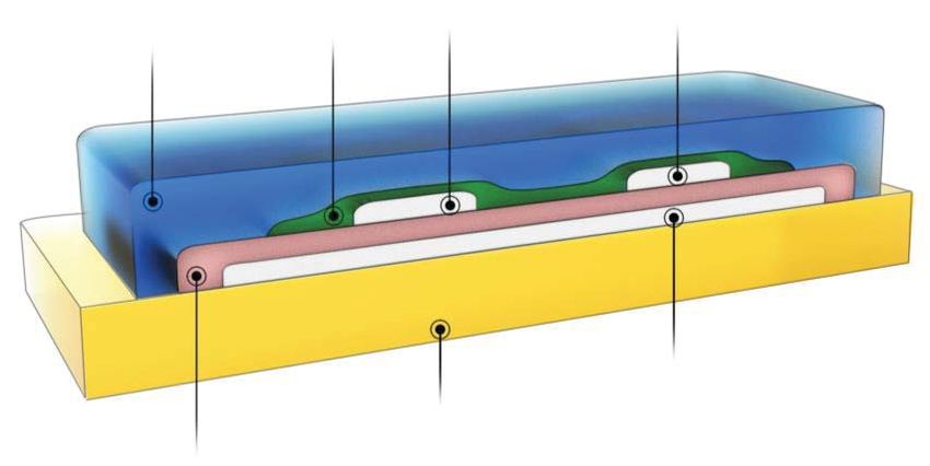
as the semiconductor (Fig. 1A), which exhibits were carried out by using a single inkjet printer ads per square centimeter. Qt and D t can be
fast growth (50 mm) tool. affected by defects in the semiconductor bulk
and has a lower HOMO level than pentacene or The SB-OTFT demonstrated a near-zero thresh- (e.g., grain boundaries and stacking faults)
other derivatives (22) to yield a good Schottky old voltage (VT = −0.01 V) (Fig. 1B), along with and at the semiconductor-dielectric interface
barrier (>0.2 eV) (19, 21). Polyvinyl cinnamate an ultrasteep subthreshold slope of SS = 60.2 mV (e.g., interface roughness and atomic species
was used as the dielectric layer to provide a per decade (Fig. 1C) that approached the theo- or vacancies on dangling bonds). The relatively
smooth interface between the semiconductor retical thermionic limit (20): large semiconductor crystals in the thin-film
and dielectric, thus minimizing carrier trapping transistor (TFT) channel (>50 mm, providing
and scattering (23). A fluoropolymer encapsulation SStheoretical ¼ lnð10Þvth good coverage over the channel) (fig. S2E) sub-
mV
layer (CYTOP) protected the device from envi- ¼ 59:6 ðat T ¼ 300 KÞ ð1Þ stantially reduce grain boundaries and stacking
ronmental effects. Silver was used for the metal decade faults, compared to those in the amorphous
parts. All of these materials were formulated as where vth = kBT/q is thermal voltage. In or micropolycrystalline phases. The printed
inks with good jetting properties (fig. S1), and addition, this steep SS is repeatable (fig. S3). polymer dielectric layer was free of dangling
all of the fabrication steps for the individual The small VT and steep SS resulted from the bonds and provided a smooth semiconductor-
SB-OTFTs and amplifier circuits reported here low trap density (20): dielectric interface (with roughness of 2.1 Å)
(fig. S2C). This was comparable to the roughness
Qt
VT ¼ VT;theoretical þ ð2Þ of the silicon–silicon dioxide interface in state-of-
1 Ci the-art complementary metal oxide semiconductor
Electrical Engineering Division, Department of
Engineering, University of Cambridge, 9 JJ Thomson and technologies. Thus, reducing the defect den-
Avenue, Cambridge CB3 0FA, UK. 2Department of Clinical sity to a very low level gives the best values for
Neurosciences, University of Cambridge, Cambridge q2 Dt
SS ¼ SStheoretical 1 þ ð3Þ VT and SS. Furthermore, the variation in these
Biomedical Campus, Cambridge CB2 0QQ, UK.
3
Ci
Cambridge Touch Technologies, 154 Cambridge Science values between devices was much less than for
Park, Cambridge CB4 0GN, UK. 4Suzhou Institute of where Qt is the trap carrier density in coulombs other vacuum deposition–based TFT technologies
Biomedical Engineering and Technology, Chinese Academy
per square centimeter, Dt is the defect trap den- (Fig. 1, D and E, and table S1). TFTs with a large
of Sciences, Suzhou 215163, China. 5Acxel Tech, 184
Cambridge Science Park, Cambridge CB4 0GA, UK. sity per electron volt and square centimeter, Ci are effective in reducing VT and SS (24) but
*Corresponding author. Email: an299@cam.ac.uk and Ci is the gate insulator capacitance in far- lead to higher operating currents. Although this
Jiang et al., Science 363, 719–723 (2019) 15 February 2019 2 of 5R ES E A RC H | R E PO R T
Fig. 3. Stability and reliability. (A) Measured transfer characteristics for (E) Measured transfer characteristics under light exposure and (F) photo-
a TFT in storage under ambient conditions for the times indicated and current (Iphoto in amperes per micrometer) and DVT for different wave-
(B) change in absolute threshold voltage (DVT) and change in relative trans- lengths (400 to 800 nm). (G) Measured SB-OTFT current noise under
conductance efficiency [D(gm/ID)] as a function of time. (C) Measured different direct current biases (IDC). (H) SNRs in the near-threshold and
transfer characteristics under negative bias stress (VGS = VDS = −3 V) for the subthreshold regimes and input-referred voltage noise density at 100 Hz.
stress time indicated and (D) DVT and D(gm/ID) as a function of stress time. a-Si, amorphous silicon.
boosts the switching speed in logic circuits, it z0 is a coefficient that describes the modula- gain (defined as A i = g mro ) (25) resulting
does not benefit the low-power, low-frequency tion of Schottky barrier height by VGS (19). Feff from the high transconductance and output
operation of analog sensor interfaces. showed a good initial Schottky barrier of ~0.51 eV resistance.
We investigated the nature of the defect and a high barrier-lowering factor of z0 = 1.24. Both the transconductance and output re-
density and of the Schottky barrier through This result suggests that charge-carrier injection sistance had an exponential dependence, with
the density of states (DOS) (see Fig. 2A) and the was mainly by thermionic emission, with smaller an inverse proportionality, on –VGS because of
effective Schottky barrier height (Feff). These contributions from thermionic field emission the response of SB-TFTs in the subthreshold
results suggest that the DOS comprises a small and tunneling (see the inset of Fig. 2B). Above a regime (Fig. 2C), as was also the case previously
and constant background of deep states (gdeep = certain VGS level (in the case shown at –0.34 V), with an inorganic SB-TFT (19). In comparison
6.59 × 1014 cm−3 eV−1, where gdeep is deep-state barrier lowering saturated and the transistor be- with other TFT technologies, the SB-OTFT trans-
density), a broad spectrum of delocalized states haved ohmically in the above-threshold regime. conductance and output resistance are about
with a characteristic energy of 24.8 meV near vth, This change occurred when the source-side 10 times as high at similar currents: gm = 3.8 ×
and a steeply rising number of localized tail depletion width reached just a few nanometers 10−8 S and ro = 3.2 × 10¹⁰ ohms at IDS = 1 nA
states with a characteristic energy of 6.7 meV. and allowed charge carriers to tunnel through (1–6, 24, 26–28). The intrinsic gain Ai was
In addition, because the DOS was dominated
pffiffiffiffiffiffiffiffiffiffiffiffiffiffiffiffiffiffiffiffiffiffiffi the Schottky barrier (fig. S5C) (20, 21). The small determined from the theoretical expression (19)
by extended states (according to E EHOMO, defect density and the presence of a good Schottky Ai ¼ SStheoretical vsat
nexp nv , where n is the ideality fac-
SS
where E is energy), there was a clear mobility barrier in the subthreshold regime were pre- th
edge for energies above the HOMO level (i.e., requisites for high transconductance (mutual tor (here, n = 1.6). These devices showed a high
E > EHOMO), characteristic of a small overall conductance gm) and output resistance (ro). and constant value for Ai of ~1100 in the sub-
DOS. Because the semiconductor surface po- The near-zero VT was important for low- threshold regime (Fig. 2D), which is much larger
tential (ϕS) cannot be neglected in low-voltage power operation, whereas the ultrasteep SS than that of the inorganic SB-TFT and Si metal
TFTs, this term was included in the DOS cal- was important for high transconductance (gm = oxide semiconductor field-effect transistor be-
culation (eqs. S5 to S23). @IDS/@VGS) and transconductance efficiency (gm/ cause of the ultrasteep SS. More notably, gm/IDS
The source-side Schottky barrier height (Feff) IDS) (eqs. S2 and S3). In addition, the SB-OTFT for the SB-OTFT was ~38.2 S/A, approaching
decreased with increasing –VGS, so that the operation was channel-length independent with the theoretical limit for TFT technologies of
drain current (IDS) was modulated by the gate a large output resistance (ro = @VDS/@IDS) (Fig. q/kBT (i.e., 38.7 S/A at T = 300 K). The high
bias. Feff could be extracted from temperature- 1F), which was provided by the Schottky bar- gm/IDS (indicating a large gm at low IDS) was
dependent I-V measurements (fig. S6). In the rier at the source-semiconductor contact. Thus, essential for an amplifier circuit to achieve high
subthreshold regime, Feff = z0VGS + Feff,0, where the SB-OTFT could provide a high intrinsic gain at low power. The SB-OTFT reported here
Jiang et al., Science 363, 719–723 (2019) 15 February 2019 3 of 5R ES E A RC H | R E PO R T
that found in typical amorphous Si- and metal
oxide–based TFTs and two orders of magnitude
lower than that in conventional OTFTs (table S1)
(32). The root-mean-square
qffiffiffiffiffiffiffiffiffiffi noise voltage referred
to the gate hv2gn i for all noise sources isR ES E A RC H | R E PO R T
RE FE RENCES AND N OT ES 22. M. Kano, T. Minari, K. Tsukagoshi, Appl. Phys. Lett. 94, 143304 (2009). 1D-NEON 685758, and BET-EU 692373. C.J. acknowledges doctorate
1. R. A. Street, Adv. Mater. 21, 2007–2022 (2009). 23. C. Jiang, H. Ma, D. G. Hasko, X. Guo, A. Nathan, Adv. Electron. scholarship support from the China Scholarship Council (CSC) and the
2. A. Nathan et al., Proc. IEEE 100, 1486–1517 (2012). Mater. 3, 1700029 (2017). Cambridge Commonwealth, European and International Trust and
3. K. Nomura et al., Science 300, 1269–1272 (2003). 24. H. Klauk, U. Zschieschang, J. Pflaum, M. Halik, Nature 445, fellowship support from the IEEE Electron Device Society. Author
4. J. F. Wager, Science 300, 1245–1246 (2003). 745–748 (2007). contributions: C.J., H.W.C., X.C., H.M., and A.N. conceived
5. D. H. Kim et al., Science 333, 838–843 (2011). 25. B. Razavi, Design of Analog CMOS Integrated Circuits (McGraw- of and designed the overall experiments. C.J. and H.W.C. carried
6. T. Someya, Z. Bao, G. G. Malliaras, Nature 540, 379–385 (2016). Hill, 2001). out experiments and collected related data. C.J. was the only human
7. A. Campana, T. Cramer, D. T. Simon, M. Berggren, F. Biscarini, 26. M. J. Powell, IEEE Trans. Electron Devices 36, 2753–2763 (1989). subject for the eye tracking study, and H.W.C. recorded the experiment.
Adv. Mater. 26, 3874–3878 (2014). 27. S. D. Brotherton, Semicond. Sci. Technol. 10, 721–738 (1995). X.C. and C.J. contributed to circuit simulation and theoretical
8. D. Khodagholy et al., Nat. Commun. 4, 1575 (2013). 28. R. Martins et al., Adv. Mater. 23, 4491–4496 (2011). analysis. C.J., H.W.C., and A.N. initiated the study. C.J., H.W.C., X.C.,
9. Y. Kim et al., Science 360, 998–1003 (2018). 29. W. H. Lee, H. H. Choi, D. H. Kim, K. Cho, Adv. Mater. 26, H.M., D.H., and A.N. analyzed all the data and co-wrote the paper. All
10. T. Sekitani, U. Zschieschang, H. Klauk, T. Someya, Nat. Mater. 1660–1680 (2014). authors discussed the results and commented on the manuscript.
9, 1015–1022 (2010). 30. H. Sirringhaus, Adv. Mater. 21, 3859–3873 (2009). Competing interests: The authors declare no competing interests.
11. J. Xu et al., Science 355, 59–64 (2017). 31. X. Jia, C. Fuentes-Hernandez, C.-Y. Wang, Y. Park, B. Kippelen, Data and materials availability: All data are available in the main text
12. H. Nishide, K. Oyaizu, Science 319, 737–738 (2008). Sci. Adv. 4, eaao1705 (2018). or the supplementary materials.
13. P. D. Mitcheson, E. M. Yeatman, G. K. Rao, A. S. Holmes, 32. T. Moy et al., IEEE J. Solid-State Circuits 52, 309–321 (2017).
T. C. Green, Proc. IEEE 96, 1457–1486 (2008). 33. D. Mantini, M. G. Perrucci, C. Del Gratta, G. L. Romani, M. Corbetta,
Proc. Natl. Acad. Sci. U.S.A. 104, 13170–13175 (2007). SUPPLEMENTARY MATERIALS
14. W. Gao et al., Nature 529, 509–514 (2016).
15. T. Sekitani et al., Nat. Commun. 7, 11425 (2016). 34. M. Brown et al., Doc. Ophthalmol. 113, 205–212 (2006). www.sciencemag.org/content/363/6428/719/suppl/DC1
16. H. Sirringhaus et al., Science 290, 2123–2126 (2000). 35. S. Hillaire, A. Lécuyer, R. Cozot, G. Casiez, “Using an eye- Materials and Methods
17. L. Feng, C. Jiang, H. Ma, X. Guo, A. Nathan, Org. Electron. 38, tracking system to improve camera motions and depth-of-field Supplementary Text
186–192 (2016). blur effects in virtual environments,” in 2008 IEEE Virtual Figs. S1 to S12
18. M. Singh, H. M. Haverinen, P. Dhagat, G. E. Jabbour, Adv. Mater. Reality Conference, Reno, NV, 8 to 12 March 2008 (IEEE, Tables S1 and S2
22, 673–685 (2010). 2008), pp. 47–50. References (36–61)
19. S. Lee, A. Nathan, Science 354, 302–304 (2016). Movie S1
20. S. M. Sze, Physics of Semiconductor Devices (Wiley, ed. 2, 1981). ACKN OWLED GMEN TS
21. Y. Xu, H. Sun, Y.-Y. Noh, IEEE Trans. Electron Devices 64, Funding: We are grateful for the generous support from EPSRC under 14 October 2018; accepted 15 January 2019
1932–1943 (2017). project EP/M013650/1 and the EU under projects DOMINO 645760, 10.1126/science.aav7057
Jiang et al., Science 363, 719–723 (2019) 15 February 2019 5 of 5Printed subthreshold organic transistors operating at high gain and ultralow power
Chen Jiang, Hyung Woo Choi, Xiang Cheng, Hanbin Ma, David Hasko and Arokia Nathan
Science 363 (6428), 719-723.
DOI: 10.1126/science.aav7057
Low-power organic transistors
For internet-of-things applications, transistors that deliver high signal amplification (high gain) at low power will
help conserve power and extend battery life. Jiang et al. used inkjet printing to fabricate an organic transistor in which
silver metal contacts form a low Schottky barrier (less than 0.2 electron volt) with an organic semiconductor. The
transistor delivered gain near the theoretical limit at a power below 1 nanowatt and detected electrophysiological signals
from the skin with a wearable device.
Science, this issue p. 719
Science (print ISSN 0036-8075; online ISSN 1095-9203) is published by the American Association for the Advancement of
Science, 1200 New York Avenue NW, Washington, DC 20005. 2017 © The Authors, some rights reserved; exclusive
licensee American Association for the Advancement of Science. No claim to original U.S. Government Works. The title
Science is a registered trademark of AAAS.You can also read


