Semiconductor Supply Chain Deep Dive Assessment U.S. Department of Energy Response to Executive Order 14017, "America's Supply Chains"
←
→
Page content transcription
If your browser does not render page correctly, please read the page content below
Semiconductor
Supply Chain Deep Dive Assessment

U.S. Department of Energy Response to Executive
Order 14017, “America’s Supply Chains”

February 24, 2022
(This page intentionally left blank)
SEMICONDUCTOR SUPPLY CHAIN DEEP DIVE ASSESSMENT

About the Supply Chain Review for the
Energy Sector Industrial Base
The report “America’s Strategy to Secure the Supply Chain for a Robust Clean Energy Transition” lays out the
challenges and opportunities faced by the United States in the energy supply chain as well as the federal
government plans to address these challenges and opportunities. It is accompanied by several issue-specific deep
dive assessments, including this one, in response to Executive Order 14017 “America’s Supply Chains,” which
directs the Secretary of Energy to submit a report on supply chains for the energy sector industrial base. The
Executive Order is helping the federal government to build more secure and diverse U.S. supply chains, including
energy supply chains.

To combat the climate crisis and avoid the most severe impacts of climate change, the U.S. is committed to
achieving a 50 to 52 percent reduction from 2005 levels in economy-wide net greenhouse gas pollution by 2030,
creating a carbon pollution-free power sector by 2035, and achieving net zero emissions economy-wide by no
later than 2050. The U.S. Department of Energy (DOE) recognizes that a secure, resilient supply chain will be
critical in harnessing emissions outcomes and capturing the economic opportunity inherent in the energy sector
transition. Potential vulnerabilities and risks to the energy sector industrial base must be addressed throughout
every stage of this transition.

The DOE energy supply chain strategy report summarizes the key elements of the energy supply chain as well
as the strategies the U.S. government is starting to employ to address them. Additionally, it describes
recommendations for Congressional action. DOE has identified technologies and crosscutting topics for analysis
in the one-year time frame set by the Executive Order. Along with the policy strategy report, DOE is releasing
11 deep dive assessment documents, including this one, covering the following technology sectors:

    •   carbon capture materials,
    •   electric grid including transformers and high voltage direct current (HVDC),
    •   energy storage,
    •   fuel cells and electrolyzers,
    •   hydropower including pumped storage hydropower (PSH),
    •   neodymium magnets,
    •   nuclear energy,
    •   platinum group metals and other catalysts,
    •   semiconductors,
    •   solar photovoltaics (PV), and
    •   wind

DOE is also releasing two deep dive assessments on the following crosscutting topics:
   • commercialization and competitiveness, and
   • cybersecurity and digital components.

More information can be found at www.energy.gov/policy/supplychains.

                                                       iii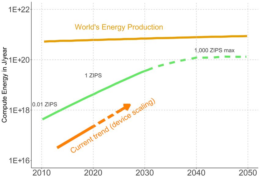
SEMICONDUCTOR SUPPLY CHAIN DEEP DIVE ASSESSSMENT

Acknowledgments
The U.S. Department of Energy (DOE) acknowledges all stakeholders that contributed input used in the
development of this report – including but not limited to federal agencies, state and local governments, U.S.
industry, national labs, researchers, academia, non-governmental organizations, and other experts and
individuals. DOE also issued a request for information (RFI) to the public on energy sector supply chains and
received comments that were used to inform this report. The authors acknowledge input and guidance from
Tsisilile Igogo of the DOE Office of Policy and National Renewable Energy Laboratory, the lead organizer of
the overall effort.

Principal Authors
Margaret, Mann, National Renewable Energy Laboratory
Vicky, Putsche, National Renewable Energy Laboratory

Contributors
Bauer, Diana, DOE Advanced Manufacturing Office, DOE office of Energy Efficiency and Renewable Energy
Buchanan, Heather, National Renewable Energy Laboratory
Diamond, David, Advanced Manufacturing Office, DOE office of Energy Efficiency and Renewable Energy
[Detailee from U.S. Geological Survey]
Hefner, Al DOE Advanced Manufacturing Office, DOE office of Energy Efficiency and Renewable Energy
Kaarsberg, Tina, DOE Advanced Manufacturing Office, DOE office of Energy Efficiency and Renewable
Energy
Keavney, Dava, DOE Advanced Manufacturing Office, DOE office of Energy Efficiency and Renewable
Energy
Mehta, Jeremy, DOE Advanced Manufacturing Office, DOE office of Energy Efficiency and Renewable
Energy
Nguyen, Ruby, Idaho National Laboratory
Smith, Braeton, Argonne National Laboratory
Syers, Paul, DOE Advanced Manufacturing Office, DOE office of Energy Efficiency and Renewable Energy
Xu, Kaifeng, National Renewable Energy Laboratory

Reviewers
Blouin, Dorothea, Department of Commerce, International Trade Administration
Crisostomo, Noel, DOE Office of Policy
Granite, Evan, DOE Office of Fossil Energy and Carbon Management
Luke, Myers, Department of Commerce, International Trade Administration
McIntosh, Kathryn, DOE Office of the General Counsel
Norville, Irene, DOE Office of the General Counsel
Tarter, J.B., DOE Office of the General Counsel

                                                     iv
SEMICONDUCTOR SUPPLY CHAIN DEEP DIVE ASSESSSMENT

List of Acronyms
 AMO         U.S. Department of Energy’s Advanced Manufacturing Office

 ASIC        application specific integrated circuits

 ATP         assembly, testing, and packaging

 CAGR        compound annual growth rate

 CHIPS       Creating Helpful Incentives to Produce Semiconductors

 DBC         direct bonded copper

 DOE         Department of Energy

 EO          Executive Order

 EPA         Environmental Protection Agency

 GaN         gallium nitride

 GDP         gross domestic product

 ESIB        Energy Sector Industrial Base

 EV          electric vehicle

 HV          high voltage

 HVDC        high-voltage direct current

 IDM         integrated device manufacturer

 IP          intellectual property

 PE          power electronics

 PFAS        per- and polyfluoroalkyl substances

 PV          photovoltaic

 R&D         research and development

 RDD&CA      research, development, demonstration, and commercial application

 SIA         Semiconductor Industry Association

 SiC         silicon carbide

 SME         semiconductor manufacturing equipment

                                                   v
SEMICONDUCTOR SUPPLY CHAIN DEEP DIVE ASSESSSMENT
SRC Semiconductor Research Corporation
TRL technology readiness level
TSMC Taiwan Semiconductor Manufacturing Company
TSV through-silicon-via
WBG wide bandgap
ZIP 10 21 (‘zetta’) compute instructions per second
viSEMICONDUCTOR SUPPLY CHAIN DEEP DIVE ASSESSSMENT
Executive Summary
In February 2021, President Biden signed Executive Order (EO) 14017, “America’s Supply Chains,” directing
seven executive agencies to evaluate the resilience and security of the nation’s critical supply chains and to craft
strategies for six industrial bases that underpin America’s economic and national security. See Sec. 3(b) of E.O.
14017. As part of the one-year response to EO 14017, the U.S. Department of Energy (DOE), through the
national laboratories, conducted evaluations of the supply chains that encompass the Energy Sector Industrial
Base, with a particular focus on technologies required to decarbonize the U.S. by 2050.
This report focuses on one of these technologies, semiconductors, both conventional and wide bandgap (WBG)
power electronics (PE). As noted in the 100-Day report, conventional semiconductors are a keystone technology
that are essential for the operation of nearly every electronic device, including those that are critical to
decarbonization, such as electric vehicles (EVs), industrial and building applications, and electricity generation
and end use. In addition, power electronics have been applied to industrial equipment to improve energy
efficiency and enhance controllability. Power electronics have also been used to improve the reliability of data
centers and critical infrastructure, including the stabilization of the electric grid while subjected to disturbances.
Increasingly, power electronics are being used to integrate renewable energy and battery storage systems,
enabling new grid services and the development of microgrids. It is estimated that 30% of the electricity used in
the U.S. passes through power electronic devices, and studies suggest that this number could reach 80% as power
electronics are deployed in more markets. Nearly all forms of electrified transportation will depend on power
electronics. Power electronic systems utilize high-capacity semiconductor devices at their core. The continued
growth in power electronics depends on sustained innovation in the semiconductor industry.
The U.S. Energy Sector Industrial Base will require radical transformations to decarbonize by 2050, and the
growth, energy efficiency, and security of the semiconductor supply chain also must transform.
The current semiconductor industry has a complex, competitive, and highly integrated international supply chain
in which the United States has historically enjoyed a dominant position, but where this position has been eroding
over time as described in the 100-Day report. This report conducted a risk assessment of the domestic
semiconductor supply chain that is focused on energy-industrial-applications and identified several
vulnerabilities. The three most critical vulnerabilities are listed below.
• Impacts of Explosive Growth: Decarbonization efforts will increase the demand for renewable energy and
its supporting infrastructure, including both conventional semiconductor and WBG power electronic supply
chains. The demand for products that will use both WBG semiconductors and conventional semiconductors
in the future is projected to increase by more than an order of magnitude by 2050 (e.g., wind 23-fold; EV-
68-fold increases) (Larson, et al., 2020). The current lack of domestic manufacturing capacity and access to
raw materials will be exacerbated. In fact, current projected global silicon production cannot keep pace with
this growth, and it is likely that other supply chains will be stretched as well. The EV sector could be
especially impacted due to the rising semiconductor use in in the vehicles as well as the necessary charging
infrastructure.
viiSEMICONDUCTOR SUPPLY CHAIN DEEP DIVE ASSESSSMENT
• Significant and rapidly rising energy demand of semiconductors during use 1 : the potential climate
impacts of the use phase of semiconductors was identified in as a concern (Semiconductor Research
Corporation, 2021) (U.S. Department of Energy Advanced Manufacturing Office, 2021-2). The global
energy use of products featuring semiconductors has doubled every three years since 2010 primarily due to
the accelerating use of semiconductors in all facets of our modern economy and the deceleration of energy
efficiency increases due to miniaturization. This exponential growth in energy use is projected to accelerate
even more due to: 1) increased electrification from decarbonization, noted above and 2) the exponential
growth in energy-intensive computer applications (e.g., artificial intelligence).
o With the explosion in use of semiconductor technologies in all sectors, especially the energy sector,
the performance and efficiency of semiconductors has a direct effect on the performance and
efficiency of technologies in those other sectors.
o Artificial intelligence algorithms are doubling their power every two months, and semiconductor
energy use just for Bitcoin mining uses more electricity than some European countries, with a 1-
year doubling time (U.S. House of Representatives' Committee on Energy and Commerce, 2022).
• Decreasing manufacturing base – In 1995, 26% of global semiconductor manufacturing capacity was
located in the United States, this has decreased to 10% by 2020 (European Semiconductor Industry
Association (ESIA), 2021). Another segment of the supply chain that is becoming more important is
packaging in the form of advanced packaging and the United States could fall behind in this area if current
trends hold.
To address these vulnerabilities, DOE has identified the following opportunities:
• Investment in the development and deployment of silicon carbide (SiC) WBG PE focused on the
higher voltage (>1700 V) applications that are critical to utility-scale renewable energy deployments.
Although the United States invented SiC WBG PE technology and is a leader in this area, this advantage
could be lost in the rapidly evolving and highly competitive WBG PE industry. One method to maintain
and perhaps improve the competitiveness of the U.S. WBG PE industry is to enable production of
significantly higher performance and higher efficiency domestically produced WBG PE devices to
supplant imported silicon-based PE devices. Such efforts to increase U.S. manufacturing of WBG
semiconductor power devices are a significant opportunity for the United States and could also provide
a strategic advantage for U.S. electric equipment manufacturers through integration with a local U.S.
supply chain for advanced WBG power semiconductors. This integration will provide product
differentiation (e.g., smaller footprint, higher efficiency, and speed) in rapidly growing electric
equipment markets such as electric vehicles (EV), EV charging stations, wind, and solar generators, as
well as equipment for flexible AC and DC power delivery.
• Investment in research, development, demonstration, and commercial application (RDD&CA)
for conventional semiconductors with a biennial energy efficiency doubling goal. Because of the
unsustainable increase (i.e., a doubling every three years) in the energy use of key energy-related
semiconductor applications a new “Moore’s law” for energy efficiency is required to guide future
1
The use phase of large electronic devices (e.g., servers) is by far the largest source of carbon emissions in the device’s life cycle (Global Electronics
Council, 2021).
viiiSEMICONDUCTOR SUPPLY CHAIN DEEP DIVE ASSESSSMENT
generations of semiconductor investments. This goal for successive generations of semiconductors-- to
double energy efficiency of semiconductor use every two years or faster for the next 20 years also could
help reestablish U.S. leadership in semiconductor manufacturing and would support Biden-Harris
Administration electrification and decarbonization goals. Several recent studies have documented that
ten generational doubling or a 1000x improvement in energy efficiency is technically achievable
(Semiconductor Research Corporation, 2021); (Shankar, 2021). If aggressive effort and significant
investment in the RDD&CA for more energy efficient semiconductors is not undertaken soon, however,
it could affect the United States’ ability to reduce carbon emissions as rapidly, economically, and
efficiently as possible.
• Promote opportunities for training, education, and certification for U.S.-based workers to ensure
that they are prepared to be a part of the domestic semiconductor industry, including the burgeoning
WBG PE industry.
Pursuing these opportunities would address the three key vulnerabilities listed above, complement the
recommendations outlined to help the U.S. regain its dominant position in this critical area of the energy sector.
Find the policy strategies to address the vulnerabilities and
opportunities covered in this deep dive assessment, as well as
assessments on other energy topics, in the Department of Energy 1-
year supply chain report: “America’s Strategy to Secure the Supply
Chain for a Robust Clean Energy Transition.”
For more information, visit www.energy.gov/policy/supplychains.
ixSEMICONDUCTOR SUPPLY CHAIN DEEP DIVE ASSESSSMENT
Table of Contents
1 Introduction ..........................................................................................................................1
1.1 Technology Description..................................................................................................................................... 1
1.2 Global Market Assessment................................................................................................................................ 2
2 Supply Chain Mapping............................................................................................................7
2.1 Technology Overview........................................................................................................................................ 7
2.2 Conventional Semiconductor Supply Chain Segments................................................................................. 8
2.3 Wide Band Gap Semiconductor Supply Chain .............................................................................................. 9
3 Supply Chain Risk Assessment ............................................................................................... 12
3.1 Conventional Semiconductor Risk Assessment........................................................................................... 13
3.2 Wide Bandgap Power Electronics Risk Assessment................................................................................... 13
3.3 Key Vulnerabilities (Near Term).................................................................................................................... 15
3.4 Key Vulnerabilities (Longer Term) ............................................................................................................... 19
3.5 Key Focus Areas...............................................................................................................................................19
4 U.S. Opportunities and Challenges........................................................................................... 21
4.1 Key Opportunities.............................................................................................................................................21
4.2 Key Challenges .................................................................................................................................................22
5 Conclusions ........................................................................................................................ 22
xSEMICONDUCTOR SUPPLY CHAIN DEEP DIVE ASSESSSMENT
List of Figures
Figure 1. Semiconductor study scope……………………………………………………………………. .........2
Figure 2. End-use market share ($million) for semiconductors…………………………………………. ..... ... 3
Figure 3. 2020 SiC power device by market……………………………………………………………… ......... 4
Figure 4. 2020 GaN power device by market…………………………………………………………….. .......4
Figure 5. Today's WBG operating voltage and applications………………………………………………....... 4
Figure 6. GaN device demand by sector………………………………………………………………….. Error!
Bookmark not defined.
Figure 7. Projected SiC device demand by sector………………………………………………………… ....... 5
Figure 8. Semiconductor Supply Chain. ............................................................................................8
Figure 9. Simplified Supply Chain for WBG Semiconductors. ...............................................................9
Figure 10. Total Energy of Computing............................................................................................ 16
Figure 11 Global demand for memory and storage using silicon wafers. ................................................ 17
xiSEMICONDUCTOR SUPPLY CHAIN DEEP DIVE ASSESSSMENT
List of Tables
Table 1. Projected increase in end-use technologies due to decarbonization ..............................................6
Table 2. Risk assessment matrix for WBG power electronics. .............................................................. 14
xii1 Introduction This document builds on the work conducted in the “America’s Strategy to Secure the Supply Chain for a Robust Clean Energy Transition” 100-Day report in response to EO 14017. Here, the U.S. Department of Energy (DOE), through the national laboratories, conducted evaluations of the supply chains that encompass the Energy Sector Industrial Base (ESIB) The U.S. ESIB will require radical transformations to decarbonize by 2050, including renewable energy generation from carbon-neutral sources combined with zero-emission transportation. While efficient clean energy and zero-emission transportation technologies are available to help achieve these goals, they currently rely on raw materials sold in opaque and volatile global markets and often concentrated in geopolitically sensitive areas. Furthermore, midstream stages of supply chains, such as material processing and component manufacturing, may be concentrated in foreign countries with complicated geopolitical relationships with the United States. DOE’s Advanced Manufacturing Office (AMO) has particular interest in evaluating the supply chain risk and resilience of semiconductors 2 . In 2021, the supply chain for semiconductors was evaluated as part of the 100-Day Reviews under EO 14017 (The White House, 2021). This report builds on this earlier work by focusing on semiconductor applications and needs in the energy sector. Semiconductors are a keystone technology in the energy sector as they are essential for the operation of nearly every electric vehicle, recharging station, and wind turbine as well as the entire electrical grid. Semiconductors are also critical to the American economy, contributing over $246.4 billion to the gross domestic product (GDP) of the United States in 2020 (Semiconductor Industry Association (SIA), 2021). With an export value of $49 billion, they were the fourth largest U.S. export in 2020 behind aircraft, refined oil, and crude oil (Semiconductor Industry Association (SIA), 2021). Wide-bandgap (WBG) power electronics (PE) are a small component (i.e., 0.1%) of this important industry; however, they are set for explosive growth to help meet the demands of decarbonization through electrification. Continued development of this technology is required to move it to high voltage (>1700 V) applications to meet the demands of the energy sector. This report provides an overview of the semiconductor supply chain, both conventional (i.e., silicon-based) and WBG semiconductors. It augments the previous semiconductor supply chain work in the 100-Day report (The White House, 2021) by focusing on the energy sector and it takes a deeper dive on WBG PE. Like the 100-Day report, it conducts a risk assessment followed by identifying the opportunities and challenges in addressing those risks. 1.1 Technology Description Semiconductors are made from elements such as silicon, or from compounds such as silicon carbide (SiC). During the fabrication process, small amounts of other materials—called ‘dopants’ are added, which cause 2 Although semiconductor materials are used in photovoltaics, these are covered in another supply chain report by the Solar Energy Technology Office and will not be covered here. For this report, “semiconductor” will refer to all semiconductors, except those in photovoltaics.
SEMICONDUCTOR SUPPLY CHAIN DEEP DIVE ASSESSSMENT
significant changes in the electronic properties of the material. This study will focus on semiconductors used in
applications that are important for the decarbonization of the energy sector. These include:
• WBG semiconductors (e.g., SiC and gallium nitride (GaN)) that control, convert, and condition power
flow for electric vehicles (EVs), electrified industrial technologies (such as industrial heat pumps), and other
renewable energy applications such as wind and solar generators.
• Conventional semiconductors (e.g., silicon-based) that control data flow for energy efficiency and
renewable energy applications, including EVs, integrated wireless sensor systems for energy-efficient
manufacturing, energy efficiency in buildings, and other renewable energy technologies.
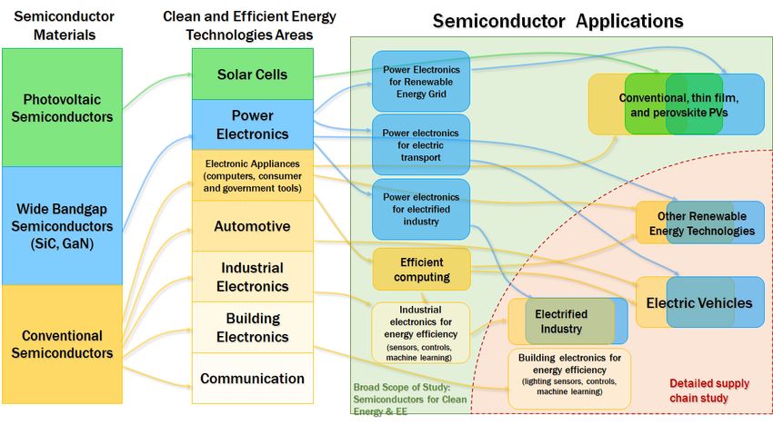
A high-level view of the types of semiconductors 3 , their differing applications and those addressed in this study
is shown in Figure 1.
Figure 1. Semiconductor study scope. 4
1.2 Global Market Assessment
1.2.1 Current Market
The overall global semiconductor market was valued at $553 billion in 2021, up from $440 billion in 2020, an
increase of over 25% (World Semiconductor Trade Statistics (WSTS), 2021). The breakdown of conventional
3
As noted earlier, PV semiconductors for solar energy production are excluded from this study because they will be addressed separately in the report from
the Solar Energy Technologies Office.
4
Note this is not to scale: Conventional (~$550 billion)>>PV (~$100 billion)>>WBG (~$1 billion) in market size (World Semiconductor Trade Statistics
(WSTS), 2021); (Yole Développement, 2021);
2SEMICONDUCTOR SUPPLY CHAIN DEEP DIVE ASSESSSMENT
semiconductors in 2020 by end-use sector is shown in Figure 2. Computing and communication are about equal
in size and comprise the major end uses of semiconductors, representing over 60% of global market value.
Industrial and automotive uses, covered in this report, comprise 12% and 11.4% of the global market value,
respectively.
Go vernment
4. 6
A utomotive
50. 1 Co mp uting
142. 2
I ndustrial
52. 9
Co nsumer
El e ctronics
53
Co mmunication
137. 6
Figure 2. End-use market share ($million) for semiconductors.
Source: (Semiconductor Industry Association (SIA), 2021)
For a more detailed discussion of the semiconductor market, refer to the 100-Day report.
While global revenues of faster, more energy-efficient WBG semiconductors—SiC and GaN—has grown
significantly from $0.2 billion in 2015 (PowerAmerica, 2020), together they still comprised less than 5% of the
power device market in 2020 which is still is dominated by silicon-based power electronics (Yole
Développement, 2021). The 2020 market value of WBG power devices was estimated at $0.6 billion or roughly
0.1% of the overall semiconductor market (Yole Développement, 2021). The market for WBG is expected to
grow significantly by 2030 as key applications such as wind energy and EVs are expected to grow from a few
percent to more than 50% of the market. Conversely, in 2019 semiconductors (WBG and conventional)
comprised about 4% of the value of a new premium car. By 2030, they are expected to comprise >20% of the
value (Intel, 2021).
The current market share of each of the major WBG technologies by market sector is shown below in Figure 3
and Figure 4 (Yole Développement, 2021). The market sectors for each type of WBG semiconductor are
significantly different, with GaN obtaining most of its revenue from consumer electronics, while SiC has a strong
presence in automotive, energy, and industrial applications.
3SEMICONDUCTOR SUPPLY CHAIN DEEP DIVE ASSESSSMENT
Te l ecom and Tr a nsportation, 4% Te l ecom &
I nfrastructure I nfrastructure
11% 16% I ndustrial
Others 16%
0%
Others
I ndustrial A utomotive 9%
14% 42%
Mo bile &
Co nsumer
Ene rgy 59%
25%
Co nsumer, 4%
Figure 4. 2020 SiC power device by market. Figure 3. 2020 GaN power device by market.
Source: (Yole Développement, 2021) Source: (Yole Développement, 2021)
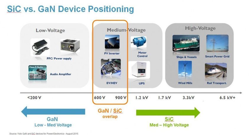
The primary driving force behind the difference in applications is the semiconductors’ operating range. As shown
in Figure 5, both semiconductors perform well between 600 and 900 V, but SiC devices also operate at much
higher voltages.
Figure 5. Today's WBG operating voltage and applications.
Source: (Yole Developpement, 2015)
One of the areas of current application overlap between GaN and SiC is in the EV sector. GaN devices are being
used for non-traction (i.e., onboard charging) applications while SiC is focused on traction inverter applications
within this sector. SiC devices are operating up to 1700 V onboard vehicles; and 1200- and 1700-V applications
4SEMICONDUCTOR SUPPLY CHAIN DEEP DIVE ASSESSSMENT
are being developed for EV propulsion inverters. SiC is also being developed for PV power applications and
wind.
Significant effort is underway to develop thick epitaxy SiC wafer manufacturing technology that can be used to
produce devices that operate at even higher voltages (much greater than the 1700 V technology widely available
today). The ability to use a WBG semiconductor in higher-voltage applications would expand the use of WBG
power semiconductors in rapidly growing renewable energy applications (e.g., wind power), and could penetrate
other critical markets such as generic high-voltage direct current (HVDC) application.
Although the technology for thick SiC wafer epitaxy (i.e., suitable for up to 10 kV) has already been developed,
a few issues preventing its widespread adoption. The biggest issue for this technology is its cost effectiveness
due to immature manufacturing methods and the lack of high-capacity facilities. In addition, advanced
packaging for the power modules is also needed, specifically direct bonded copper (DBC) insulator substrates
are needed to provide thermal management for the high voltage (>10 kV) WBG power modules. Because of the
limitations of silicon semiconductors at the high voltages, this market is currently limited. It has significant
growth potential due to the increased need from energy applications that can be exploited by improving the
performance of SiC power devices. Bulk GaN (single crystalline GaN substrate wafer) development is also
underway for use in high-performance devices. Because bulk GaN work is still in the research stage at a very
low technology readiness level (TRL), there is an opportunity to establish a strong and secure supply chain in
this area.
1.2.2 Market Projections
In November 2021, The World Semiconductor Trade Statistics (WSTS) (2021) reported that it expected that the
global semiconductor market growth would be 25.6% in 2021 to $553 billion compared to a 6.8% increase in
2020. It is projected to increase by another 8.8% in 2022 to reach $601 billion.
Although SiC and GaN power devices today are a small fraction of the total power sector, demands for both
technologies are expected to increase significantly and are expected to comprise almost 20% of the power device
market by 2026, with SiC reaching 14% and GaN at almost 5% (Yole Développement, 2021). Overall, the WBG
power electronics market is expected to grow from $0.6 billion in 2020 to $2.2‒$3.1 billion by 2026 (Markets
and Markets, 2021); (Yole Développement, 2021), a CAGR of 20%‒36%. Both markets are also expected to
diversify, with GaN expanding into automotive and SiC growing its industrial and automotive markets. Figure
6 and Figure 7 show the projected growth of both technologies by end-use sector.
$1,200 $4,000
GaN Device Demand $M
SiC Device Demand $M
$1,000
$3,000
$800
$600 $2,000
$400
$1,000
$200
$0 $-
2019 2020 2021 2022 2023 2024 2025 2026 2019 2020 2021 2022 2023 2024 2025 2026
Automotive Energy Consumer Industrial
Transportation Energy
Industrial Mobile & Consumer
Figure 7. GaN device demand by sector. Figure
Figure 8.
6. Projected
AutomotiveProjected SiC
SiC device
device demand
demand
Telecom by
by sector.
sector.
and Infrastructure
Source: (Yole Développement, 2021) Source:
Source: (Yole
(Yole Développement,
Développement, 2021)
2021)
5SEMICONDUCTOR SUPPLY CHAIN DEEP DIVE ASSESSSMENT
These significant growth rates (i.e., 8.8% annual increase for conventional semiconductors and >20% CAGR for
WBG) are under current business-as-usual scenarios without considering deep decarbonization strategies.
While the total demand for conventional semiconductors and WBG power electronics under deep
decarbonization scenarios has not yet been determined, rough estimates can be derived from key subsectors. In
November 2021, the U.S. Department of State and U.S. White House released The Long-Term Strategy of the
United States (LTS), which lays out how the United States can reach its goal of net-zero emissions no later than
2050 and was submitted to the United Nations Framework Convention on Climate Change (UNFCCC) at the
26 th Conference of the Parties. The LTS illustrates many plausible pathways through 2050 to achieve a net-zero
emissions economy and offers insights into what the overall energy system for the United States could look like
between now and 2050 under a range of assumptions about the evolution of technological costs, economic
growth, and other drivers to 2050. (U.S. Department of State and the U.S. Executive Office of the President,
2021). Other groups have done similar analyses. For example, the Net Zero America report (Larson, et al., 2020)
outlines five different cases to achieve net zero by 2050. In both studies, the demand for EVs, wind and other
renewable power, and heat pumps (commercial and residential) increases significantly, and these increases are
expected immediately. For example, in the Larson study, wind and solar generating capacity are expected to
grow fourfold to 600 GW to supply half of U.S. electricity, up from 10% today. Increases in each of the
technologies will in turn increase the demand for semiconductors. Table 1 summarizes the projected increase of
some technologies that rely on semiconductors from both studies.
Table 1. Projected increase in end-use technologies due to decarbonization
Technology U.S. Long Term Strategy Net Zero Study
Wind Powera 4-7.5x increase in renewable generation 6x‒28x increase in installed capacity
EVs ~100% of light-duty vehicles electrified 40x‒63x increase in the number of EVs and
and the associated charging associated charging infrastructure
infrastructure
Commercial / 5x increase in industrial electrification Increase heat pumps by 3x in commercial
Industrial buildings by 2030
a
The Wind Energy Technology Office is currently funding a study at the National Renewable Energy Laboratory to look at all the material requirements for
wind energy, including semiconductors. When these results are available, they will be used to update the table.
Sources: Larson et. al (2020); U.S. Department of State and Executive Office of the President
Although it is unlikely that the increase in conventional semiconductors due to decarbonization will accelerate
to the same extent as these electric and electrification technologies, it is certain that the overall growth rate of
both types of semiconductors will dwarf even what is predicted for clean energy technologies due to the
explosion of memory needed for the data deluge and other exponentially increasing semiconductor applications
(e.g., 5G+ communications). The Semiconductor Research Corporation (SRC) estimates that memory and
storage demand will increase by a factor of greater than 100 by 2030.
In some cases, such as with EVs, the growth rate could be even higher than projected in Table 1 as EVs have
more semiconductors, especially WBGs than conventional vehicles. CISION PR Newswire estimates that the
value of semiconductors (conventional and WBGs) in EVs is 2.3 times the value in conventional vehicles
(CISION PR Newswire, 2021). The United States International Trade Commission (Lawrence & VerWey, 2019)
estimates that difference to be even greater, with conventional vehicles containing $300 worth of semiconductors
and hybrid electric vehicles containing from $1,000 to $3,500 worth of semiconductors. Further illustrating
6SEMICONDUCTOR SUPPLY CHAIN DEEP DIVE ASSESSSMENT
demand beyond the EVs themselves, the effective integration of charging loads into the electric grid requires
power semiconductors to convert and condition the power flow between grid and vehicle battery, and
microelectronics within the charging equipment to communicate session data and to manage power flows
(Harper, 2021).
2 Supply Chain Mapping
This section includes descriptions of the supply chains of both technologies. The 100-Day report (The White
House, 2021) provided a detailed look at the supply chain of conventional semiconductors, including all
segments, and will not be repeated here – only a high-level description is provided. More detail will be provided
for the WBG supply chain where it differs from that of conventional semiconductors.
In the following discussion, unless noted otherwise, market share, sales, etc. of the segments are attributed by
the headquarters of the company, even if the physical location of the facility is in another country. The market
values are for 2019 unless otherwise specified.
2.1 Technology Overview
The market and supply chain for semiconductors is global and extremely complex. Numerous companies across
the globe, specializing in one or more steps of the process, are involved. As noted in the 100-Day report (The
White House, 2021), the designing, fabricating, and packaging of a semiconductor product takes up to 100 days,
including 12 days of transit, and can cross international borders 70 times (i.e., travelling to the same countries
more than once).
Most supply chains can be characterized by five main segments: raw materials, processed materials,
subcomponents, product, and end-of-life recycling/reuse. The complexity of semiconductors, however, require
several additional supply chain segments: design, semiconductor manufacturing equipment (SME), and
assembly, testing, and packaging (ATP), including advanced packaging. Similarly, due to the continual rapid
evolution of semiconductor technology, research and development (R&D) is also included in the supply chain.
For simplicity, reuse/recycling will not be covered in this analysis; however, end-of-life issues are becoming
more important as e-waste is the world’s fastest growing waste stream.
Figure 8 shows the semiconductor supply chain, including examples of materials moving between segments.
Raw material extraction, material processing, and subcomponent manufacturing for the semiconductor supply
chain is similar to most other supply chains. The difference comes in the fabrication or production stages, as
specialized equipment or SME is required along with specialized design tools and software.
As shown in the orange blocks in Figure 8, semiconductor production has three main steps: design, fabrication,
and ATP. These steps can be conducted by a single company, known as an integrated device manufacturer
(IDM), or by different companies. When production is conducted by different companies, a fabless firm (i.e., a
design firm without a dedicated fabrication facility) conducts the design and contracts with a foundry to fabricate
the chip with packaging at an outsourced semiconductor assembly and test (OSAT) firm.
7SEMICONDUCTOR SUPPLY CHAIN DEEP DIVE ASSESSSMENT
Research and
Raw Materials
Development
Silicon,
IDM
Iron
Design Processed
EDA and Core IP
(Fabless) Materials
Steel,
PFAS
Polysilicon
EUV, wafer HF, PFAS
manufacturing,
Photomasks, Purified
Semiconductor deposition
wafers, CMP lead,
Manufacturing tools Fabrication Subcomponent
copper
Equipment & (Foundry) Materials
Tools
Testing Lead frames,
tools, Bonding
assembly wires,
inspection Assembly Testing interconnect,
tools I/O materials Packaging
and Packaging
Materials
Materials (OSAT)
Fabrication
Processes
SME Diode,
Integrated End Use
R&D and EDA Circuit
End Use
Figure 9. Semiconductor Supply Chain.
Advanced packaging includes technologies for heterogeneous integration (combined functionality of logic and
memory within a single device) such as putting chiplets and/or more than one integrated circuit into a single
package. It also includes vertical stacking for 3D architectures with through-silicon-vias (TSVs). These types of
advanced packaging allow higher transistor density at the package level instead of the chip level and it enables
a wider variety of chip functions in a single package – both of which can greatly increase energy efficiency. Of
course, efficiency improvements also are needed for monolithic chips.
2.2 Conventional Semiconductor Supply Chain Segments
The 100-Day report mapped the conventional semiconductor supply chain in detail and will not be repeated here.
However, the high-level summary of each domestic semiconductor supply chain segment is outlined below.
• Design: The United States has a robust and world-leading semiconductor industry but depends on
limited sources of intellectual property (IP), labor and manufacturing.
8SEMICONDUCTOR SUPPLY CHAIN DEEP DIVE ASSESSSMENT
• Semiconductor Fabrication: The United States lacks sufficient fabrication capacity and relies on
sources in Asia for production.
• Assembly, Test and Packaging and Advanced Packaging: The United States relies on foreign ATP
companies in Asia. Although the United States and its partners have advanced packaging capabilities,
it lacks the ecosystem for developing advanced packaging technologies
• Fabrication Materials: The United States and its allies have strong capabilities in wet chemical and
electronic gas production. Foreign suppliers dominate the markets for silicon wafers, photomasks and
photoresists, but these products are manufactured in many places, including the United States.
• Semiconductor Manufacturing Equipment: The United States has a significant share of global
production of most front-end SME with the exception of lithography equipment. While it has a
significant share of back-end testing equipment, it has a small market share in packaging equipment.
2.3 Wide Band Gap Semiconductor Supply Chain
As noted earlier, the basic supply chain segments for WBG semiconductor-based power electronics are the same
as those for conventional semiconductors. The differences lie in the products and processes within those
segments. For example, much of the manufacturing equipment for (older node) conventional semiconductors
can be used for WBG power electronics manufacturing. The most significant differences are in the raw materials,
subcomponents, end products, and packaging.
Figure 9 shows the overall process steps, as well as some representative materials for each step, which are then
described in more detail below.
Polysilicon
gallium
Silicon Epi-wafers, Packaging
Electronic gases CMP, materials
Carbon photomask
Acids s
Raw Materials Processed Fabrication ATP End Product
Materials Subcomponents
Figure 10. Simplified Supply Chain for WBG Semiconductors.
Detailed analyses were not conducted for each supply chain sector of the WBG PE supply chain because for
many of the sectors (e.g., SME), the components are similar, if not the same as those for conventional
semiconductors that were analyzed in the 100-Day report. In addition, because the size of the market for WBG
PE is so small compared to that for conventional semiconductors, it is likely that those sectors are similar to the
larger market. Thus, only raw materials, processed materials, ATP and the final product form are discussed.
2.3.1 Raw Materials
One of the primary raw materials for SiC WBG semiconductors is quartzite or silicon, found in abundance across
the globe as sand (U.S. Geological Survey, 2022). Demand for silicon for electronics applications such as PVs
and displays (even though they don’t require quite the same high purity) as well as for glass, and concrete (which
have even lower silicon purity requirements), has grown so fast that the cheapest and most abundant silicon
9SEMICONDUCTOR SUPPLY CHAIN DEEP DIVE ASSESSSMENT
sources are being over-exploited. As the prices of the lowest cost sources of sand have increased, mining of river
bottoms, beaches, and forest lands has become profitable, leading to environmental damage and, in some cases,
labor exploitation (Beiser, 2019). Tracking of global sand mining, legal and illegal, is unreliable and likely
missing significant operations (Bendixen, Best, Hackney, & Lars, 2019). Insofar as growing demands for high-
purity silicas will impact semiconductor manufacturing, paying attention to environmental and social impacts,
as well as calls to regulate sand mining (Gallagher & Peduzzi, 2019), will be essential for supply chain resiliency.
Graphite is another raw material for SiC WBG and is available in either natural or synthetic from. Natural
graphite is obtained by mining and synthetic is made industrially from coal or petroleum coke. The United States
produces no natural graphite and has limited reserves (U.S. Geological Survey, 2022)).
Gallium is not mined in the United States and globally is currently recovered as a secondary product from
processing bauxite and zinc ores (U.S. Geological Survey, 2022). Gallium is also listed as a critical material in
the 2021 proposed critical materials list from USGS (2021 Draft List of Critical Materials, 2021). Current
production of GaN power semiconductors is limited to the low-voltage segment and only consumes a small
amount of gallium as they are made in a thin ~1µm layer of gallium grown on non-gallium substrates. If bulk
GaN substrates were to emerge in the future and be used to produce high-voltage power devices, they would
consume significantly more gallium. High voltage SiC power semiconductors have the advantage that they do
not rely in critical materials such as gallium. China dominates gallium production, producing over 90% of the
world’s gallium (U.S. Geological Survey, 2022).
In 2021, one domestic company recovered and refined high-purity gallium from imported primary low-purity
gallium metal and scrap (U.S. Geological Survey, 2022). Other companies import gallium metal and gallium
arsenide wafers.
2.3.2 Processed Materials
Processed materials for WBG semiconductors include bulk SiC boules, SiC wafer substrates, and epitaxial SiC
layers (thin and thick) grown on SiC substrate wafers. WBG processed materials also include thin GaN epitaxial
layers grown on silicon, sapphire, or SiC substrates, but thick GaN epitaxial layers would require a source of
bulk GaN boules and wafer substrates that are not yet produced at a TRL and quality suitable for power
semiconductor devices. The power semiconductor devices are fabricated in the high-quality epitaxial layer where
the substrate serves as mechanical support. Several U.S. companies produce SiC and GaN epitaxial wafers and
the United States has a very strong market position in SiC wafers. Most of the production of GaN wafers is in
Taiwan.
The two companies with the highest capacity for SiC wafers/boules are domestic companies—Wolfspeed and
II-VI. Wolfspeed has an estimated capacity of 75,000‒100,000 units per year while II-VI is estimated to have a
capacity of about 70,000 units per year. Both companies have recently announced investment in the rapid
expansion of production capacity in SiC substrates through devices. SiCrystal, which is a joint
Japanese/European Union company, has a 60,000 unit per-year capacity and the remaining companies have
capacities of 35,000 units per year and below.
The next level processed material is the SiC epi-wafer. This wafer product has been processed so that it is ready
to go to chip processing. The open SiC power epi-wafer market is dominated by Wolfspeed (United States) and
Showa Denko (Japan), each with similar market shares. Although the quality and performance of SiC with thick
epitaxy (up to 100 µm) are well established, these materials are not produced at the scale needed to meet the
demand of rapidly emerging clean energy applications.
10SEMICONDUCTOR SUPPLY CHAIN DEEP DIVE ASSESSSMENT 2.3.3 Final Product WBGs go into numerous products, primarily in the power sector. For this analysis, the product is assumed to be a WBG power device or module. As noted earlier, the WBG power device market is about $0.6 billion, and it currently is dominated by STMicroelectronics, a French-Italian company. Recently, a number of large SiC power device fabrication facilities have been announced in the U.S. including the largest in world being built in Marcy, New York by Wolfspeed (Wolfspeed, 2022). 2.3.4 Assembly Testing and Packaging and Packaging Materials Packaging of WBG power semiconductors highly leverages technology used for previous generation silicon power semiconductor devices. Low-power discrete (single die) power device packaging is almost exclusively produced off-shore and there is currently limited value added or economic benefit to packaging discrete die in the United States. On the other hand, high power and high voltage module packages are critical to the performance of WBG power semiconductor device products and U.S. companies including Wolfspeed (Fayetteville, AR), Powerex (Youngwood, PA), and GE Aviation (Pompano Beach, FL) are leading innovators. However, the production capacity of these facilities is currently much lower than similar companies abroad. Danfoss also recently built a large production capacity SiC power module package facility in Marcy, New York to serve the U.S. automotive industry. 2.3.5 U.S. Resilience and Risk The United States is the leader in SiC substrates with the greatest production capacity and the two largest suppliers, Wolfspeed and II-VI. While SiC epi-wafer is available from several companies around the world, U.S. products have the highest quality. Both companies have significant domestic expansion plans. The United States is also the leader in quality production of thick (~100µm) SiC epi-wafers, which can be used to produce devices with voltage ratings up to 10 kV that are critical for renewable generation, manufacturing scale electric power systems, and the electricity grid. While Wolfspeed’s quality is the highest, their product is expensive, and their production capacity is low. Although II-VI is looking to develop this technology in Sweden with their acquisition of Ascatron, without a second production source and significant capacity expansion, lack of thick SiC epi-wafers could become a significant supply chain bottleneck for clean energy technology advancement. GaN on Si, SiC, or sapphire is widely available and is used for optical radio frequency (RF) and
SEMICONDUCTOR SUPPLY CHAIN DEEP DIVE ASSESSSMENT

voltage levels of SiC power devices already exceeding the voltages previously possible with silicon.
Furthermore, with WBG devices operating at switching speeds of 10 to 100 times faster than possible with
silicon, the package is often the limiting factor in achieving the full potential of the WBG semiconductors. The
lack of U.S. manufacturing capability for power semiconductors packaging was a key factor leading to
offshoring of previous generations of power semiconductor devices. Going forward, U.S. investment in domestic
power module packaging fabrication facilities is essential to avoid offshoring of the WBG power semiconductor
supply chain.

Taiwan controls most of the GaN on silicon device fabrication market, whereas the U.S. is competitive in the
device design and application integration.

3 Supply Chain Risk Assessment
DOE developed a high-level methodology to identify potential supply chain risks by sector and subsector. This
methodology is described in this section and results are provided for WBG semiconductors. The 100-Day report
already conducted a supply chain risk assessment for conventional semiconductors (The White House, 2021); a
summary of the recommendations from this risk assessment are provided in the conventional semiconductor
discussion.

The raw material, processed material, and product sectors of WBG semiconductors were evaluated according to
the criteria outlined below. The SME, ATP, design and fab material sectors were not evaluated as they do not
differ considerably from the conventional semiconductor segments, which was well covered in the 100-Day
report.

The evaluation criteria are related to market (domestic and global) size and their projected growth, U.S.
manufacturing capabilities and suppliers, as well as exogenous factors such as environmental/climate or human
rights concerns that could impact the supply chain. DOE selected a measure for assessment for each criterion
and assigned a scoring scale to each resulting in a Green, Yellow, or Red score.

•       Green scores show strength and/or low risk or vulnerability and have specific, measurable values.
•       Red scores indicate a potential risk and are given when the sector does not meet the Green score.
•       Yellow scores are given if there is not enough information to determine a score.

The evaluation criteria and method of scoring are described below.

•       Significant domestic supply: Domestic supply is evaluated as significant (Green) if the domestic
market supply can meet at least 50% of the estimated domestic demand.
•       Projected significant domestic demand: The projected domestic demand is significant (Green) if the
CAGR is projected to be greater than 2% for at least five years. If the specific projected demand for a sector or
subsector cannot be determined, then the demand for the end product is used as a proxy.
•       Significant global market: If the market for the sector or subsector is greater than $5 billion, then the
market is significant and received a Green score.
•        Projected significant global market: If the CAGR for that sector is projected to be greater than 2%
for at least five years, it is considered significant, or Green. If the specific projected demand for a sector or
subsector cannot be determined, then the demand for the end product is used as a proxy.

                                                       12
SEMICONDUCTOR SUPPLY CHAIN DEEP DIVE ASSESSSMENT
• Competitiveness of the U.S. market: Domestic competitiveness is measured by the number of
domestic companies in the specific sector or subsector. Having more than three domestic companies in the sector
shows a competitive market and receives a Green score.
• Competitiveness of U.S. suppliers in the global market: U.S. suppliers are competitive if they capture
at least 30% of the global market.
• Security of supply chain: This criterion has two measures: identification as a critical mineral (U.S.
Geological Survey, 2021) or the amount imported. If the material is identified or proposed as a critical mineral
or is composed of a significant amount (>10%) of a critical mineral, then the supply is insecure. For other
materials, if the amount imported is greater than 50%, it is significant and receives a Red score.
• Environmental, climate, or human rights concerns: Here DOE addresses important external factors
that can affect the development of the supply chain. For example, if the current supply chain relies on slave or
forced labor, not only is it against international law but it makes the supply chain less resilient and makes it more
important to develop an alternative source. This criterion is more subjective than the others in that DOE did not
develop a numerical scale. However, DOE wanted to ensure that these concerns were addressed. In general, if a
sector has been identified in the literature as having significant energy demands or hazardous waste issues, etc.,
then it would be given a Red score. Similarly, if literature has identified human rights (e.g., use of slave labor)
in a sector, this will be given a Red score. If there are no identified issues, a Green score will be given. If the
sector is not known well or there are questions, then DOE gave it a Yellow score.
DOE used the risk assessment to identify vulnerabilities and to highlight subsectors that should be developed
domestically.
3.1 Conventional Semiconductor Risk Assessment
As noted earlier, the 100-Day report conducted a comprehensive risk assessment of the conventional
semiconductor supply chain. Based on this assessment, the following seven recommendations were made to
expand and secure the U.S. semiconductor supply chain:
1. Promote investment, transparency, and collaboration, in partnership with industry, to address the current
shortage
2. Fully fund the Creating Helpful Incentives to Produce Semiconductors (CHIPS) for America provisions
to promote long-term U.S. leadership
3. Strengthen the domestic semiconductor manufacturing ecosystem
4. Support small and medium enterprises and disadvantaged firms along the supply chain to enhance
innovation
5. Build a talent pipeline
6. Work with allies and partners to build resilience
7. Protect the U.S. technological advantage
3.2 Wide Bandgap Power Electronics Risk Assessment
Much of the upstream supply chain for WBG power electronics is similar to that for conventional semiconductors
(e.g., much of the equipment can be used for both products) and is not evaluated here. The following risk
assessment matrix addresses WBG power electronics for raw materials, processed materials and end products.
13You can also read