Stress engineering of boron doped diamond thin films via micro-fabrication
←
→
Page content transcription
If your browser does not render page correctly, please read the page content below

Stress engineering of boron doped
diamond thin films via micro-fabrication
Cite as: APL Mater. 9, 061109 (2021); https://doi.org/10.1063/5.0051196
Submitted: 23 March 2021 . Accepted: 31 May 2021 . Published Online: 15 June 2021

  Fabio Isa,     James P. Best,    Anna Marzegalli,     Marco Albani, Christophe Comte,   Jamie J. Kruzic,   Avi
Bendavid, et al.

ARTICLES YOU MAY BE INTERESTED IN

Origin of magnetic anisotropy, role of induced magnetic moment, and all-optical
magnetization switching for Co100−xGdx/Pt multilayers
APL Materials 9, 061110 (2021); https://doi.org/10.1063/5.0050985

MOVPE of GaN-based mixed dimensional heterostructures on wafer-scale layered 2D
hexagonal boron nitride—A key enabler of III-nitride flexible optoelectronics
APL Materials 9, 061101 (2021); https://doi.org/10.1063/5.0049306

Electrical and chemical analysis of Ti/Au contacts to β-Ga2O3
APL Materials 9, 061104 (2021); https://doi.org/10.1063/5.0051340

APL Mater. 9, 061109 (2021); https://doi.org/10.1063/5.0051196                                          9, 061109

© 2021 Author(s).
APL Materials                                                                                   ARTICLE           scitation.org/journal/apm

    Stress engineering of boron doped diamond
    thin films via micro-fabrication
    Cite as: APL Mater. 9, 061109 (2021); doi: 10.1063/5.0051196
    Submitted: 23 March 2021 • Accepted: 31 May 2021 •
    Published Online: 15 June 2021

    Fabio Isa,1,2,a)   James P. Best,3,4 Anna Marzegalli,5                   Marco Albani,6         Christophe Comte,1
                     3
    Jamie J. Kruzic,      and Avi Bendavid1,7

    AFFILIATIONS
    1
      CSIRO Manufacturing, 36 Bradfield Road, Lindfield, New South Wales 2070, Australia
    2
      Department of Physics and Astronomy, Macquarie University, Sydney, New South Wales 2109, Australia
    3
      School of Mechanical and Manufacturing Engineering, University of New South Wales (UNSW Sydney), Sydney,
      NSW 2052, Australia
    4
      Max-Planck-Institut für Eisenforschung GmbH, Max-Planck-Straße 1, D-40237 Düsseldorf, Germany
    5
      L-NESS and Dipartimento di Fisica, Politecnico di Milano, via Anzani 42, 22100 Como, Italy
    6
      L-NESS and Department of Materials Science, Università di Milano-Bicocca, via Cozzi 55, 20125 Milano, Italy
    7
      School of Materials Science and Engineering, University of New South Wales (UNSW, Sydney), Sydney, NSW 2052, Australia

    a)
     Current address: Evatec AG, Hauptstrasse 1A, 9477 Trübbach, Switzerland. Author to whom correspondence should be
    addressed: fabio_isa@outlook.com

    ABSTRACT
    In this paper, a novel approach is presented to tailor the stress properties of diamond thin films via boron doping and micro-fabrication of
    bridges using focused ion beam milling. The experimental data, based on detailed confocal micro-Raman investigations, are supported and
    interpreted through finite element method calculations of the stress distribution at mechanical equilibrium. These results indicate that appro-
    priate design of microbridge geometries, together with boron doping, would allow the material stress to be largely enhanced or diminished
    compared to non-patterned thin films. Our approach, together with a deterministic incorporation and positioning of diamond color centers,
    may open novel opportunities to tailor the optical and spin properties of diamond-based quantum devices through stress engineering.
    © 2021 Author(s). All article content, except where otherwise noted, is licensed under a Creative Commons Attribution (CC BY) license
    (http://creativecommons.org/licenses/by/4.0/). https://doi.org/10.1063/5.0051196

          Diamond has incredible potential for functional utilization in          When using top-down micro-fabrication approaches for sili-
    optical, photonic, and electronic devices based on its high conduc-      con and germanium, the production of strain enhanced microbridge
    tivity and chemical inertness while remaining optically transpar-        (MB) structures has been demonstrated as effective in enhancing
    ent.1,2 With some mechanical properties (e.g., hardness and elastic      the material properties.6,7 Indeed, such solutions can improve the
    modulus) reach the limits of known materials, mechanical alter-          opto-electronic properties of semiconductors, tuning the nature of
    ation (i.e., machining) of diamond is a constant challenge. While        the material bandgap and enabling the fabrication of group-IV
    deposition of diamond-based thin films circumvents several bulk-         integrated lasers on silicon.8,9
    scale fabrication hurdles, tuning the mechanical strain state with            Additionally, boron doping of diamond (boron-doped dia-
    the corresponding properties of diamond layers remains non-trivial.      mond, BDD) can lead to advantageous semi- or super-conducting
    Precise control of the strain in diamond thin films would be of          properties, together with the traditional benefits of diamond,
    paramount importance to tune the resonance frequency and qual-           making it attractive for sensing applications in challenging
    ity factor of micro-resonators.3 Focused ion beam (FIB) milling has      environments.10 Previously, electron-beam lithography has
    been utilized to further manipulate diamond coatings to fabricate        been used to nanopattern BDD to investigate the robustness
    single-crystal diamond micro-cantilevers4 and MEMS5 for sensing          of its superconducting properties.11 However, further devel-
    applications.                                                            opments are needed to capitalize on these concepts of strain

APL Mater. 9, 061109 (2021); doi: 10.1063/5.0051196                                                                                       9, 061109-1
© Author(s) 2021
APL Materials                                                                                       ARTICLE               scitation.org/journal/apm

    enhancement and boron doping when producing practical diamond
    structures.
          Accordingly, in this paper, we present a novel method of con-
    trolling the stress in diamond layers by means of epitaxial growth of a
    stressed BDD layer, together with FIB milling microbridge structure
    fabrication. This approach exploits first the biaxial stress generated
    in the BDD layer due to the different lattice and thermal expansion
    coefficients12 compared to the intrinsic diamond substrate.13–15 Sec-
    ond, two MBs with specific geometries are fabricated, enhancing or
    reducing the initial stress to reach the mechanical equilibrium con-
    dition. The non-homogeneous stress distribution results in a vari-
    ation of the phonon resonance energy, which is measured by the
    spectral position change in the diamond Raman peak.16 The exper-
    imental results are corroborated by finite element method (FEM)
    calculations, which elucidate the stress enhancement/relaxation pro-
    cess induced by the two different MB geometries (hereafter termed
    as MB1 and MB2).
          The samples consisted of two BDD thin films grown by
    microwave chemical vapor deposition epitaxy on (001) diamond
    single crystals (see the supplementary material). The BDD thickness
    for MB1 was 500 nm and for MB2 was 750 nm, while the B concen-
    tration in both BDD layers (H terminated surface) was determined
    from four-point probe I–V curves,17,18 resulting in a resistivity of 10    FIG. 1. (a) Perspective-view SEM image of MB1. The dark areas below PL, B,
    mΩ cm, which indicated [B] = 0.8 at. %.                                    and PR are FIB undercuts. (b) Optical microscope image, taken from the Raman
          The FIB milled (see the supplementary material) MBs were             spectrometer, of the MB1 structure. The black dashed rectangle indicates the area
                                                                               measured by confocal Raman mapping. The length l along [100] and width w along
    undercut an angle between the [001] crystal direction and the Ga+          [010] of TL and TR regions are indicated in black. (c) Same as (b) but for the MB2
    beam of 45○ , resulting in wedge-shaped MBs with a bottom surface          structure.
    free of substrate contact. Final polishing with lower currents was
    performed to achieve the final geometry, as indicated in Fig. 1(a),
    for MB1.
          The stress distribution in the MBs was analyzed by scan-            light to confirm the single-crystal nature of the deposited diamond
    ning confocal Raman microscopy using a Renishaw inVia spec-               material.
    trometer equipped with a 514 nm laser and a 50× objective                       The geometries of MB1 and MB2 structures are depicted in
    with NA = 0.9. The laser spot was focused on the BDD surface,             the perspective-view SEM and optical microscope images shown in
    and the lateral and depth resolutions were (1.22 × λ)/(2 × NA)            Fig. 1. MB1 consists of five different regions marked as left triangu-
    ∼ 350 nm and λ/NA2 ∼ 630 nm, respectively. The sample was                 lar pad (TL—red), left pad (PL—blue), bridge (B—yellow), right pad
    scanned along the x//[100] − y//[010] directions by means of              (PD—blue), and right triangular pad (TR—red). In contrast, MB2
    a piezo-stage in steps of 100 nm, covering an area of at least            consisted of only three regions: triangular pad (TL—red), bridge
    40 × 10 μm2 . At each x–y position, a Raman spectrum was acquired         (B—yellow), and right triangular pad (TR—red). The dark trape-
    between 1200 and 1800 cm−1 . The diamond Raman peak centered at           zoidal areas above and below the bridges are undercut materials by
    ω (ωD = 1332 cm−1 for fully relaxed diamond)19,20 was then fit using      FIB milling. The trapezoidal shape was required to efficiently sputter
    a Lorentzian function L, as given in the following equation, where        the material and avoid re-deposition during the FIB milling process.
    γ is the peak width, a and b are the intensity and offset constants,      The black dashed rectangles in (b) and (c) indicate the area mapped
    respectively:                                                             by confocal Raman. Table I reports the length l along [100], width
                                                                              w along [010] [see Fig. 1(a)], and thickness h along [001] of the
                          L = a × γ/[(ω − ωD )2 + γ2 ] + b.            (1)    different MB regions.
    The spectral position of the Raman peak is influenced by the stress             Confocal Raman spectra were then taken from the regions
    σ xx + σ yy distribution in the BDD thin layer16 according to Eq. (2),    highlighted with black dashed rectangles in Figs. 1(b) and 1(c).
    while the stress component σ zz along z is relaxed through the (001)      Figure 2(a) reports in blue the Raman spectrum, obtained in the cen-
    free surface, as given in Eq. (3) (for more details, see the chapter      ter of the MB1–TR region. It is dominated by the first order Raman
    “stress–Raman model” in the supplementary material),                      line of diamond.21 The inset shows the Lorentzian fit function L
                                                                              (orange) of the diamond Raman peak (blue) in the spectral range
                    σxx + σyy = 1.21(GPa/cm−1 ) × (ωD − ω),            (2)    between 1320 and 1345 cm−1 . Notably, the sp2 carbon Raman sig-
                                                                              nal at higher wavenumbers is negligible, indicating the good crystal
                                        σzz = 0.                       (3)    quality of the epitaxial diamond.22 Analogous results were obtained
                                                                              across all the MB1 and MB2 regions. The fit error on the peak posi-
    The spectrometer was equipped with a rotating λ/2 waveplate (angle        tion was about 0.2 cm−1 , corresponding to a stress uncertainty of
    θ in 3○ steps) on the laser beam and a polarizer on the scattered         0.07 GPa.

APL Mater. 9, 061109 (2021); doi: 10.1063/5.0051196                                                                                                     9, 061109-2
© Author(s) 2021
APL Materials                                                                                                       ARTICLE            scitation.org/journal/apm

    TABLE I. List of MB1 and MB2 geometrical parameters (see Fig. 1) used also in FEM            Indeed, the angular fit proportional to sin2 θ (orange) matches very
    calculations. l is the region length along [100], w is the width along [010], and h is the   well with the integrated intensity of the diamond Raman peak (blue)
    thickness along [001].
                                                                                                 measured at different values of θ, indicating the absence of crystal
    Microbridge              Region             l (μm)           w (μm)             h (μm)       twins.19 The same analysis was also performed in the center of each
                                                                                                 region (TL, PL, PR, and B) of the MB1 and MB2 structures, resulting
    MB1                         TL                5.7               17                           in similar conclusions.
    MB1                         PL                9.5                5.1               2.6             The stress σ xx + σ yy was calculated by applying Eqs. (1) and
    MB1                         B                 4.3                1.7               0.9       (2) to the Raman spectra obtained by confocal mapping. Impor-
    MB1                         PR                9.5                5.1               2.6       tantly, σ xx + σ yy was also measured in the non-patterned areas about
    MB1                         TR                5.7               17                           50 μm away from the MBs, as indicated in Fig. S1. In the non-
    MB2                         TL                2.2               12.1                         patterned areas, σ xx + σ yy average values of 1.49 ± 0.04 and 1.70
    MB2                         B                17.6                1.3               0.7       ± 0.04 GPa were determined for the MB1 and MB2 samples, respec-
    MB2                         TR                2.2               12.1                         tively (see the supplementary material). The stress variation between
                                                                                                 the two samples may be ascribed to the different BDD film thick-
                                                                                                 nesses of 500 and 750 nm for the MB1 and MB2 structures, which
         For backscattering confocal Raman spectroscopy with the laser                           have a relevant impact on the relaxation of the lattice and thermal
    beam parallel to the [001] diamond direction and a polarizer on                              mismatch developed during epitaxy and sample cooling to room
    the scattered beam parallel to [100], the Raman selection rules for                          temperature.24
    single crystals23 indicate that the scattered intensity is proportional                            Figure 3(a) shows the distribution of σ xx + σ yy measured in the
    to sin2 θ, where θ is the angle between the laser polarization vec-                          MB1 black dashed area marked in Fig. 1(b). The stress variation in
    tor and [100]. Figure 2(b) reports the variation of the diamond                              each MB1 region is displayed as histograms in Fig. 3(b) for TL, (c)
    Raman integrated intensity, as a function of the laser polariza-                             for PL, (d) for B, (e) for PR, and (f) for TR regions.
    tion angle θ, measured in the center of the MB1–TR region. This                                    First, the measured stress distribution is symmetric with respect
    result confirms the good epitaxial crystal quality of the BDD layer.                         to the bridge center as a direct consequence of the micro-fabrication
                                                                                                 geometry. Second, the stress varies significantly in each MB1 region
                                                                                                 compared to the average value of 1.49 GPa in the non-patterned area.
                                                                                                 It increases in B, reaching a maximum value of 1.74 GPa and an aver-
                                                                                                 age value of 1.56 ± 0.09 GPa, and it decreases in PL and PR to 0.96
                                                                                                 ± 0.07 GPa and reaches an intermediate value of 1.35 ± 0.03 GPa in
                                                                                                 TL and TR. The elastic mechanism leading to the non-uniform stress
                                                                                                 distribution in the MB structure was elucidated by FEM simulations
                                                                                                 and will be discussed later in this work.
                                                                                                       Analogously, Fig. 4(a) reports the stress σ xx + σ yy distribu-
                                                                                                 tion of MB2, measured in the black dashed rectangle highlighted in
                                                                                                 Fig. 1(c). As previously described, the geometry of MB2 differs from
                                                                                                 that of MB1 due to the lack of the rectangular pads PL and PR. The
                                                                                                 different geometric structure had a strong impact on the σ xx + σ yy
                                                                                                 distribution compared to the results of MB1 presented in Fig. 3. As
                                                                                                 indicated in the σ xx + σ yy stress histograms shown in Figs. 4(b)–4(d),
                                                                                                 while TL and TR areas had only slightly lower average stress com-
                                                                                                 pared to the non-patterned region (1.70 GPa), being 1.53 ± 0.07 and
                                                                                                 1.56 ± 0.04 GPa, respectively, the stress in region B was significantly
                                                                                                 reduced to 1.31 ± 0.04 GPa. These results clearly indicate that the
                                                                                                 stress in BDD/diamond layers can be enhanced or reduced by the
                                                                                                 appropriate choice of microbridge geometry.
                                                                                                       The mechanisms leading to the experimental results reported
                                                                                                 in Figs. 3 and 4 were elucidated by three-dimensional (3D) FEM
                                                                                                 simulations as follows: The FEM simulations were performed using
                                                                                                 the software Comsol Multiphysics. 3D models of the MB struc-
                                                                                                 tures were implemented using the experimental geometrical param-
                                                                                                 eters reported in Table I. The stress field was calculated by solv-
                                                                                                 ing the mechanical equilibrium problem, set according to the stress
      FIG. 2. (a) Raman spectrum obtained from confocal spectroscopy in the center               conditions measured by Raman spectroscopy in the non-patterned
      of the MB1–TR region. The inset shows a magnification (black dashed rectangle)             regions for the BDD layer (see the supplementary material). The
      of the experimental data (blue) and Lorentzian fit curve L (orange) in the spec-           equilibrium state was numerically determined by benefitting of the
      tral range between 1320 and 1345 cm−1 . (b) Integrated intensity of the diamond            zero-stress condition provided by the free surfaces of the system.
      Raman peak (blue) and its angular fit (orange) as a function of the laser beam
                                                                                                 The meshes were refined in the MB region where a better resolu-
      polarization angle θ recorded in the center of the MB1–TR region.
                                                                                                 tion of the stress tensor was required [see Figs. S5(a) and S5(d)].

APL Mater. 9, 061109 (2021); doi: 10.1063/5.0051196                                                                                                             9, 061109-3
© Author(s) 2021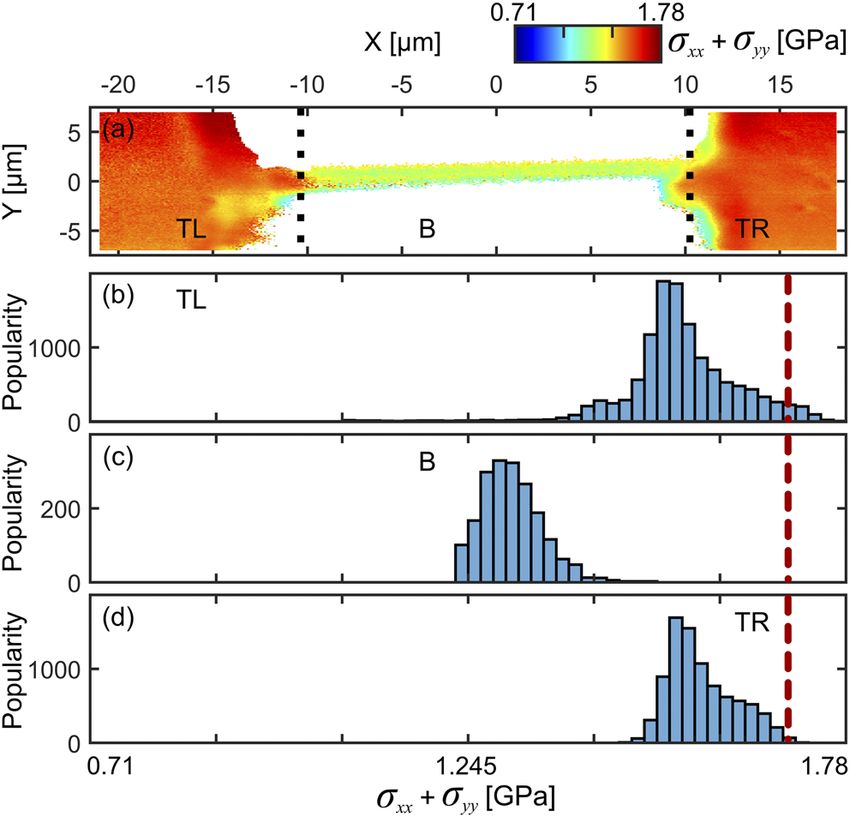
APL Materials                                                                                                        ARTICLE               scitation.org/journal/apm

                                                                                                FIG. 4. (a) Color-coded map of the σ xx + σ yy stress distribution measured from
                                                                                                confocal Raman mapping of the MB2 structure. Three different regions, labeled as
                                                                                                TL, B, and TR, are indicated with black dashed vertical lines. (b) Popularity his-
                                                                                                togram of the σ xx + σ yy stress distribution in the TL region. (c) and (d) Same
                                                                                                as (b) but for the B and TR regions, respectively. The histogram bin width is
                                                                                                1.8 × 10⁻² GPa, and the dark-red dashed line represents σ xx + σ yy in the
                                                                                                non-patterned area.

      FIG. 3. (a) Color-coded map of the σ xx + σ yy stress distribution measured from         further elucidated by the color maps for the in-plane (x − [100] and
      confocal Raman mapping of the MB1 structure. Five different regions, labeled as          y − [010] directions) σ xx and σ yy components of the stress tensor, as
      TL, PL, B, PR, and TR, are separated by black dashed vertical lines. (b) Popularity      shown in Figs. 5(b) and 5(c), respectively. The σ xx component of the
      histogram of the σ xx + σ yy stress distribution in the TL region. (c)–(f) Same as (b)
      but for the PL, B, PR, and TR regions, respectively. The histogram bin width is          stress is fully concentrated in the thinnest bridge region B, while the
      1.8 × 10⁻² GPa, and the orange dashed line represents σ xx + σ yy in the non-            orthogonal component σ yy is almost fully relaxed through the free
      patterned area.                                                                          surfaces, thus resulting in uniaxial stress distribution in B. Impor-
                                                                                               tantly, the FEM simulations demonstrate that the σ xx + σ yy stress in
                                                                                               the B region of MB1 is significantly higher than the average value in
    The lattice parameter and elastic constants of diamond and BDD                             the non-patterned area, proving that this MB configuration can be
    were taken from previously published results.13–15                                         exploited to locally increase the diamond stress.
          The FEM simulations reported in Figs. 5(a) and 5(d) qualita-                              Conversely, by changing the geometry of the suspended micro-
    tively resemble and corroborate the experimental σ xx + σ yy results                       bridge from MB1 to MB2, where the wide rectangular pads PL and
    of MB1 and MB2 reported in Figs. 3 and 4, respectively. Indeed,                            PR are missing, the stress enhancement effect in the thin bridge
    Fig. 5(a) reports the σ xx + σ yy color map of MB1: compared to the                        region B is lost. Indeed, the MB2 color map of σ xx + σ yy shown in
    non-patterned area, σ xx + σ yy is (i) significantly enhanced within                       Fig. 5(d) indicates that the thin bridge B has much lower σ xx + σ yy
    the thin microbridge region B, (ii) strongly reduced in the wide PL                        with respect to the nearby non-patterned area. Analogously, the TL
    and PR regions, and (iii) slightly relaxed in the triangular regions TL                    and TR partially relax their stress due to the free surfaces. This FEM
    and TR. The stress distribution in the MB1 regions can be explained                        result is in very good agreement with the experimental data reported
    as follows: First, the creation of free surfaces by FIB milling allows                     in Fig. 4. A more detailed examination of the FEM results further
    stress relaxation by lattice bending (see Fig. S5), which is not possible                  reveals the role of the MB2 geometry in the stress relaxation process.
    in a non-patterned film. The stress relaxation process is more effec-                      By considering the components of the stress tensor for the in-plane
    tive in the rectangular wide PL and PR regions than in the TL and                          directions, namely, σ xx and σ yy along the x − [100] and y − [010]
    TR areas. Second, the stress, particularly along the x − [100] direc-                      directions, it is observed that not all stress components decrease
    tion, is efficiently transferred from the wide PL and PR pads to the                       in the region B with respect to the non-patterned film. Indeed, as
    thinner and smaller volume bridge region B, deforming and bend-                            shown in Fig. 5(f), the free surfaces normal to the y − [010] and
    ing it (see Fig. S5). This stress transfer process leads to the higher                     z − [001] (not shown here) directions very efficiently relax the σ yy
    value of stress for region B, as shown in Fig. 5(a). This mechanism is                     and σ zz components through lattice bending and contraction along

APL Mater. 9, 061109 (2021); doi: 10.1063/5.0051196                                                                                                                      9, 061109-4
© Author(s) 2021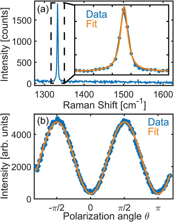
APL Materials ARTICLE scitation.org/journal/apm
diamond stress (∼0.1 to 0.4 GPa) is beneficial to improve the opti-
cal and spin coherence time by controlling the effect of the thermal
phonon bath without lowering the operating temperature.27
Additional information on substrate preparation and diamond
film growth, focus ion beam milling, the stress–Raman model, stress
evaluation in the non-patterned film, and finite element method
calculations of material stress can be found in the supplementary
material.
This work was performed, in part, at the Melbourne Centre
for Nanofabrication (MCN) in the Victorian Node of the Australian
National Fabrication Facility (ANFF). F.I., A.M., and M.A. are grate-
ful to Dr. Emiliano Bonera for the support to interpret the Raman
results. F.I. thanks Dr. W. Purches, Dr. M. Vepsalainen, Dr. L. J.
Rogers, Professor T. Volz, Dr. A. Stacey, Dr. V. R. Adineh, and
Dr. T. van der Laan for fruitful discussions. We acknowledge the
CSIRO postdoctoral fellowship program and CSIRO Manufacturing
for financial support.
DATA AVAILABILITY
The data that support the findings of this study are available
from the corresponding author upon reasonable request.
REFERENCES
1
C. Bradac, W. Gao, J. Forneris, M. E. Trusheim, and I. Aharonovich, Nat.
Commun. 10, 5625 (2019).
FIG. 5. 3D FEM simulation of the stress distributions for MB1 and MB2 evaluated 2
N. Donato, N. Rouger, J. Pernot, G. Longobardi, and F. Udrea, J. Phys. D: Appl.
on the top (001) surface. (a) Top view color-coded map of the calculated σ xx + σ yy
Phys. 53, 093001 (2020).
stress, and (b) σ xx and (c) σ yy are the stress components of MB1. (d)–(f) Same as 3
(a)–(c) but for MB2, respectively. Y. Cao and N. Sepúlveda, Adv. Mater. Interfaces 6, 1900887 (2019).
4
B. Z. Kupfer, R. K. Ahmad, A. Zainal, and R. B. Jackman, Diamond Relat. Mater.
19, 742 (2010).
these directions [see Fig. S5(f)]. Contrarily, along the x − [100] direc-
5
M. Liao, Funct. Diamond 1, 29 (2021).
6
tion, there is no equivalent possibility for the MB structure to con- R. A. Minamisawa, M. J. Süess, R. Spolenak, J. Faist, C. David, J. Gobrecht, K. K.
Bourdelle, and H. Sigg, Nat. Commun. 3, 1096 (2012).
tract. Indeed, Fig. 5(e) demonstrates that the relaxation process of 7
M. J. Süess, R. Geiger, R. A. Minamisawa, G. Schiefler, J. Frigerio, D. Chrastina,
TL and TR (blue-relaxed regions) results in a high uniaxial stress σ xx
G. Isella, R. Spolenak, J. Faist, and H. Sigg, Nat. Photonics 7, 466 (2013).
value in the thin region B. 8
S. Wirths, R. Geiger, N. von den Driesch, G. Mussler, T. Stoica, S. Mantl, Z.
By comparing the geometry of MB2 and MB1 structures, it is Ikonic, M. Luysberg, S. Chiussi, J. M. Hartmann, H. Sigg, J. Faist, D. Buca, and
now clear that the wide rectangular pads PL and PR are necessary D. Grützmacher, Nat. Photonics 9, 88 (2015).
9
for allowing a non-uniform stress relaxation process that enhances V. Reboud, A. Gassenq, N. Pauc, J. Aubin, L. Milord, Q. M. Thai, M. Bertrand,
the σ xx + σ yy stress in the thin region B. In contrast, we demonstrated K. Guilloy, D. Rouchon, J. Rothman, T. Zabel, F. Armand Pilon, H. Sigg,
that the pad-less MB2 geometry has a significantly reduced σ xx + σ yy A. Chelnokov, J. M. Hartmann, and V. Calvo, Appl. Phys. Lett. 111, 092101
(2017).
stress in region B. 10
Y. He, H. Lin, Z. Guo, W. Zhang, H. Li, and W. Huang, Sep. Purif. Technol. 212,
In conclusion, we have demonstrated that combining boron
802 (2019).
doping, together with engineered fabrication of suspended micro- 11
E. A. Ekimov, V. A. Sidorov, E. D. Bauer, N. N. Mel’nik, N. J. Curro, J. D.
bridges, enables the control of the stress in diamond thin films. The Thompson, and S. M. Stishov, Nature 428, 542 (2004).
experimental Raman results, supported by FEM calculations, indi- 12
T. Saotome, K. Ohashi, T. Sato, and H. Maeta, J. Phys.: Condens. Matter 10,
cate that biaxial σ xx + σ yy and uniaxial σ xx stress in the microbridge 1267 (1998).
13
region can be largely enhanced or diminished by appropriate design. V. V. Brazhkin, E. A. Ekimov, A. G. Lyapin, S. V. Popova, A. V. Rakhmanina,
Indeed, if large, relaxed pads (PL and PR in MB1) are present at the S. M. Stishov, V. M. Lebedev, Y. Katayama, and K. Kato, Phys. Rev. B 74,
ends of the bridge, its uniaxial and biaxial stress is largely enhanced 140502(R) (2006).
14
compared to the non-patterned films. Conversely, if the large pads W. L. Wang, M. C. Polo, G. Sánchez, J. Cifre, and J. Esteve, J. Appl. Phys. 80,
1846 (1996).
are absent (MB2), the bridge relaxes the stress through the free sur- 15
T. Wojewoda, P. Achatz, L. Ortéga, F. Omnès, C. Marcenat, E. Bourgeois,
faces, resulting in lower stress than the non-patterned film. Our X. Blase, F. Jomard, and E. Bustarret, Diamond Relat. Mater. 17, 1302
novel approach may pave the way to the fabrication of integrated (2008).
diamond surface acoustic wave devices25 or quantum photonic sys- 16
M. H. Grimsditch, E. Anastassakis, and M. Cardona, Phys. Rev. B 18, 901
tems based on diamond color centers,1,26 where precise tuning of the (1978).
APL Mater. 9, 061109 (2021); doi: 10.1063/5.0051196 9, 061109-5
© Author(s) 2021
APL Materials                                                                                                 ARTICLE                scitation.org/journal/apm

    17                                                                                 24
       P. Ashcheulov, J. Sebera, A. Kovalenko, F. Fendrych, A. Taylor, O. Frank, L.       C. V. Falub, M. Meduňa, D. Chrastina, F. Isa, A. Marzegalli, T. Kreiliger, A. G.
    Kavan, I. Kraus, and I. Kratochvılova, Eur. Phys. J. B 86, 443 (2013).             Taboada, G. Isella, L. Miglio, A. Dommann, and H. Von Känel, Sci. Rep. 3, 2276
    18
       R. F. Mamin and T. Inushima, Phys. Rev. B 63, 033201 (2001).                    (2013).
    19                                                                                 25
       S. Prawer and R. J. Nemanich, Philos. Trans. R. Soc. London, Ser. A 362, 2537      D. Munk, M. Katzman, M. Hen, M. Priel, M. Feldberg, T. Sharabani, S. Levy, A.
    (2004).                                                                            Bergman, and A. Zadok, Nat. Commun. 10, 4214 (2019).
    20                                                                                 26
       E. J. Di Liscia, F. Álvarez, E. Burgos, E. B. Halac, H. Huck, and M. Reinoso,      S. Maity, L. Shao, S. Bogdanović, S. Meesala, Y. I. Sohn, N. Sinclair, B. Pingault,
    Mater. Sci. Appl. 04, 191 (2013).                                                  M. Chalupnik, C. Chia, L. Zheng, K. Lai, and M. Lončar, Nat. Commun. 11, 193
    21
       A. M. Zaitsev, Optical Properties of Diamond (Springer Berlin Heidelberg,       (2020).
    2001).                                                                             27
                                                                                          Y. I. Sohn, S. Meesala, B. Pingault, H. A. Atikian, J. Holzgrafe, M. Gündoǧan,
    22
       C. Casiraghi, A. Hartschuh, H. Qian, S. Piscanec, C. Georgi, A. Fasoli, K. S.   C. Stavrakas, M. J. Stanley, A. Sipahigil, J. Choi, M. Zhang, J. L. Pacheco,
    Novoselov, D. M. Basko, and A. C. Ferrari, Nano Lett. 9, 1433 (2009).              J. Abraham, E. Bielejec, M. D. Lukin, M. Atatüre, and M. Lončar, Nat. Commun.
    23
       R. Loudon, Adv. Phys. 13, 423 (1964).                                           9, 2012 (2018).

APL Mater. 9, 061109 (2021); doi: 10.1063/5.0051196                                                                                                                9, 061109-6
© Author(s) 2021
You can also read