Tetris: A Frame Perfect Game Adventure - Electrical and Computer ...
←
→
Page content transcription
If your browser does not render page correctly, please read the page content below
18-500 Final Report - March 2, 2020                                                                             Page 1 of 18

Tetris: A Frame Perfect Game Adventure
                                     Authors: Eric Chen, Alton Olson, Deanyone Su
                           Electrical and Computer Engineering, Carnegie Mellon University

     Abstract—A FPGA-based system that is capable of           2    DESIGN REQUIREMENTS
generating a modern 2-player Tetris game that largely
follows the Tetris Design Guideline, though it is not              The primary design requirement in our system is the
necessarily Guideline-compliant. This system provides          frame-perfect implementation. A typical display runs at
frame-perfect responsiveness to the user(s) in addition        60 hz. Therefore, we expect our user to see their inputs
to displaying information about both the user’s game           reflected by the display within 60  1
                                                                                                      of a second. This will
state and the opponent’s game state over VGA. The              be tested using hardware counters, which are explained in
user primarily interacts with a custom-designed, re-
                                                               depth later, in Section 4.1. In short, we measured on-chip
versible controller and receives auditory information
                                                               latency while ignoring the latency from the controller to
from an external DAC which drives a 3.5mm jack. 2-
player battles are enabled on a custom, local network          the FPGA and from the FPGA to the monitor. These are
connection over 2x20 general-purpose input/output              parameters that are outside the scope of our design.
(GPIO) pins.                                                       In terms of game mechanics, we are following the Tetris
                                                               Design Guideline for the majority of our implementation, as
     Index Terms—arcade, emulation, FPGA, frame-               described in [7]. These game mechanics are verified through
perfect, game, local area network, low-latency, network-       playtesting. While it is possible to test these inputs in sim-
ing, PCB, synthesizer, SystemVerilog, Tetris, Verilog          ulation, at the human time-scale at which these mechanics
                                                               occur, it is more efficient to playtest. Further detail of the
                                                               game mechanics are provided in Section 5.1.
1    INTRODUCTION                                                  Of course, individual small components are verified for
                                                               correctness using simulation testbenches, while more com-
    Most modern Tetris implementations rely on a CPU to
                                                               plex components are verified for correctness using hardware
express the intricacies of the fundamental game mechan-
                                                               testbenches. This enabled an efficient path towards inte-
ics. Mechanics like the Super Rotation System (SRS), De-
                                                               gration while ensuring correctness in discrete parts.
layed Auto Start (DAS), and tspins are easier to implement
                                                                   Our sound synthesizer produces “Korobeiniki”, the
and debug in a traditional software programming language.
                                                               classic Tetris background music. The music is sampled at
However, CPU-based implementations suffer from two ma-
                                                               50 KHz, slightly above the industry standard of 44.1 KHz.
jor flaws: input latency and resource contention.
                                                               This sampling rate is measured by the clock rate generated
    The input/output (I/O) stack in modern computers at-
                                                               over GPIO for the external DAC. The industry standard is
tempt to strike a balance between performance and load on
                                                               based on the Nyquist-Shannon Sampling Theorem applied
the processor to avoid wasting valuable processor time. As
                                                               to the range of human hearing (2 - 20 KHz). Sampling at
a result, I/O latency in modern systems tends to be rather
                                                               a higher rate than the standard ensures that the audible
long as most applications have no need for near-instant I/O
                                                               sound signal is recreated correctly and is not detrimental
latency. However, Tetris is one such application. The user
                                                               to the result.
expects that their input is reflected by the game state in-
                                                                   Our network is a custom protocol over a subset of the
stantaneously. This is difficult for CPU-based implementa-
                                                               GPIO pins available on our FPGAs. The requirements on
tions to service as their responsiveness is bottle-necked by
                                                               this network is that it does not interfere with the single-
their I/O stack. In our implementation we enforce that user
                                                               player mode(s) and that it can communicate the necessary
inputs must be reflected in the next frame that is loading
                                                               data within the latency of a single frame since the data
onto the monitor, a latency that we term “frame-perfect”.
                                                               it carries is to be displayed to the user. Therefore the re-
    Despite multi-core and simultaneous multi-threading                                              1
                                                               quired network latency is less than 60   of a second. The true
technologies in modern CPUs, the vast majority of pro-
                                                               requirement is somewhat less than that though, since the
grams are still largely single-threaded. This means that
                                                               data needs to be received, processed, and then prepared
the various services that run the game: the network stack,
                                                               to be shown to the user in a timely manner. The network
input handlers, game logic, etc. can interfere with each
                                                               takes advantage of the available pins to transmit data in
other and cause stalls for the queued processes. By nature,
                                                               parallel and enable more robust encoding techniques.
FPGAs are inherently parallelized and can avoid these is-
                                                                   As a side note, there are 7 types of tetrominoes in Tetris,
sues entirely. In design, the separate components, graphics,
                                                               I, O, T, J, L, S, and Z. They are cyan, yellow, magenta,
logic, networking, etc. can be built to operate indepen-
                                                               blue, orange, green, and red, respectively as depicted in
dently such that, unless logically required, no process will
                                                               [7]. They will be referred to as such for the rest of this
waits on the completion of another independent process.
                                                               document.
The cost of this parallelism is area on-chip, so our design
must reasonably fit into an economical FPGA.
18-500 Final Report - March 2, 2020 Page 2 of 18
Figure 1: Overview of the full system per FPGA. The red box indicates the components on the FPGA itself while the
blue boxes are housed on an external PCB, interfaced with via GPIO. The PCB with the audio processing middleman
and the controller interface also houses a network interface to connect to the second FPGA for Battle mode.
3 ARCHITECTURE OVERVIEW This system requires full send and receive stacks to
encode and decode data.
Our system is architected with division of labor in mind.
Given our team of 3, we wanted each contributor to be able 4. Audio Synthesis
to work in parallel as long as possible. This maximizes This subsystem is responsible for producing audio for
the efficiency of our individual work, and also reduces the the user experience. The data is pulled from the
number of errors than can occur due to miscommunication. Game Logic subsystem for sound effects as well as
With this in mind, we split our design into 5 major sections. a smaller separate module in the FPGA (not pic-
tured) to read data from a memory file to produce
1. Game Logic music. This includes a lookup table to reference notes
This subsystem is responsible for the majority of to waveforms of the correct frequency. The external
game mechanics. This holds both system state and DAC that drives the 3.5mm jack is housed on an ex-
game state. These are used to provide data as needed ternal PCB, the middleman PCB. This middleman
to other sub-systems in addition to allowing the other PCB is wired into directly using GPIO, which is then
subsystems to communicate to each other as needed. broken into components for the external DAC, the
network protocol, and the controller.
2. Graphics
This subsystem is responsible for graphical output via 5. Controllers
(S)VGA. The data pulled from the Game Logic sub- This subsystem is responsible for the primary interac-
system is re-organized into either tiles or blocks and tion with the user. The user(s) will use the controllers
rendered into an understandable form for the user. to provide inputs to the Game Logic subsystem. The
Each independent portion of the graphical output has controller has a dedicated PCB which is cabled to
a dedicated pixel driver to detail that portion of the the middleman PCB. The buttons are arranged in a
display. This reduces complexity of each individual layout that mirrors a generic pair of human hands.
pixel driver and also makes graphical errors quicker
to debug as each error can be instantly isolated to Further detail of each system is discussed in section 5.
a particular driver. This subsystem is tightly inte-It is important to note that while the network protocol is
grated with the Game Logic subsystem as the major- designed and set, the interfaces between each of the subsys-
tems is not fixed as the information that needs to be shared
ity of data that needs to be displayed is directly tied
to the game state. between each module is not static. As new mechanics are
added, the Graphics subsystem grows larger and may re-
3. Network Protocol quire more information from the Game Logic subsystem to
This subsystem is responsible for communication be- drive that graphical output. It is within expectations for
tween FPGAs. This is only used in the 2-player Bat- the system architecture to expand the interfaces for each
tle mode and communicates data over the GPIO pins. system as mechanics are added.18-500 Final Report - March 2, 2020 Page 3 of 18
4 DESIGN TRADE STUDIES
In our design, there were several decisions that each
were a trade-off of many considerations. The FPGA plat-
form we chose to use, the bandwidth of the network pro-
tocol, and the controller scheme were all chosen in pursuit
of practicality in implementation or to further enable us
to perform well in our primary metric, latency. Here we Figure 2: Latency measured by on-chip hardware counters.
detail some of the trade-offs we made and how our choice Latency is measured from valid user input detection until
performed in comparison to our theories from earlier in the the vertical sync pulse pulse of the relevant frame on the
semester. VGA interface
As a result of these two factors, we can enable a very
4.1 Latency: Handling User Inputs short turnaround on any user input, something on the or-
der of a few dozen cycles. This includes loading in the new
We used (S)VGA as our interface to the user. This in- state as a result of the user input as well as handling the
terface was chosen because it is simple to implement on aftereffects of that action, like detecting a t-spin, line clear-
an FPGA, flexible in terms of refresh-rate and resolution, ing, and sending lines to the opponent, if in the multiplayer
and the boards available to us had this interface available. mode.
While we settled on a respectable 800x600 @ 72Hz proto- Here in Fig. 2 we present the latency of our system,
col, on a faster board we could have further improved our as measured by the on-chip hardware counters. Note that
latency metrics by driving a faster pixel clock to the dis- this is a fairly pessimistic measurement of on-chip latency
play. As we discuss more further below, the majority of since the value is always ready within a few dozen cycles.
the latency to the end user is waiting for the screen to re- However, these values are displayed to the user at a fixed
fresh with updated data. A faster refresh rate could enable rate, 1 frame per display refresh. Therefore, it is more fair
this latency to shrink as the vertical sync pulse pulse comes to measure to the relevant vertical sync pulse pulse, which
more often to update the display with new data. if missed, means the pulse after the one that was missed.
Our project goal was to build a system that could reflect This waiting period is a majority of the latency experienced
a user input as quickly as possible. Monitors have a refresh by the user, but is also unavoidable by nature of the display
rate at which new data is displayed on the screen. By en- interface.
suring that our data was available as quickly as possible, we Exploring this metric a bit, this latency is intending to
guarantee that the data is displayed in the next available measure information to the user. Thus, whether the verti-
screen refresh. The critical path in handling user inputs cal sync pulse is missed is not just a function of compute
is essentially managing state, which the graphics subsys- time but also when the input is received. If the input is re-
tem then reflects onto the screen. When the user enters an ceived in the lower quarter of the screen, the input cannot
input, upon determining that the input is valid, the state possible be shown to the user since the playfield has already
change is loaded into the relevant registers immediately, been rendered. As such, it would be too generous to use
with the possible next-states pre-computed. the first vertical sync pulse seen (very quickly seen) even
This pre-computation is possible because of 2 factors: though the computed value is ready. Therefore, it is more
accurate to measure to the next vertical sync pulse. This is
1. User inputs must have a cool-down period. Without why we see a greater than 1 frame latency even though our
a cool-down, an input by the user is typically held for system is capable of producing up-to-date information well
thousands, if not millions, of cycles. This is by nature within a frame as this value is intended to portray (almost)
of human time-scales vs the on-chip clock speed. So end-to-end latency to the user.
then, an appropriate input rate is something on the
scale of millions of cycles to allow the user to react
4.2 FPGA Platform and Logic Element
to the state change that they input and then let go
of the key. Usage
We intended, from the beginning of this project, to use
2. Tetris is a simple game in comparison to something either the DE2-115 Cyclone IV FPGA or the DE0-CV Cy-
like a 2-D platformer or an arcade fighter. The re- clone V FPGA. This is because both of these boards are
ality is that, there are only so many inputs available ”pure” FPGAs in the sense that there is no SoC on-board
to the user. Then, with these very finite possibilities, that handles I/O. This is important because I/O intercon-
we can compute all the possible next states and ef- nects tend to be throughput-optimized rather than latency-
fectively let the user choose the next state they wish optimized. The SoC also introduces additional complexity
to use. This next state evaluation can be very expen- to the project overall, since we have to interact with it even
sive. The bulk of our optimization work was spent on if we would prefer direct access to various pins like VGA
this part of our project. or seven-segment displays.18-500 Final Report - March 2, 2020 Page 4 of 18
This design decision was effectively an area vs I/O that crosstalk in the wires, when sending real data, could
trade-off. We had to either design our off-board interface destroy the clock signal, resulting in clock glitching in the
to be compact enough to fit into a single GPIO port on the slave board. This is discussed more in Section 4.3.3.
DE2-115 or optimize our design to be able to fit onto the
DE0-CV. As it turns out, we were unable to optimize our 4.3.2 Error Correction and Detection
design enough to fit onto the DE0-CV, seeing as we needed
roughly 45K to 50K logic elements in our final design, even In the original design of the network protocol, we had
after optimizing our more expensive modules. This would planned to use a Hamming code to implement SECDED de-
have been nearly 90% of the available logic elements on the coding on chunks of data being sent across the GPIO pins.
board. As a result, we determined place and route on the This would have enabled the receiver on either end to de-
DE0-CV would have been (nearly) impossible to place and tect errors in the payload and wait for the re-transmission,
route. Additionally, the DE2-115 boards enabled us to syn- rather than accepting known bad data. While this code
thesize, place, and route on the ECE machines owned and would not have been impervious to every error we could
operated by the University rather than doing so on our lap- see on the ribbon cables, it would have done some work to
tops. One of the results of the COVID-19 pandemic is that reduce the visual glitches that occurred in our final imple-
one of the authors lost access to a reasonably powerful com- mentation. The final network stack did not have any error
puter and was unable to efficiently synthesize on their local correction built into the data transfer. This was left out
machine. Laptops tend to perform poorly in the relatively due to a combination of factors, primarily lack of time and
complex synthesize, place, route workflow, so working on additional complexity incurred. Having this functionality
the school servers enabled a shorter iteration cycle. Unfor- would have reduced visual glitches in the opponent’s play-
tunately, this also came with the effect that the single GPIO field that gets transmitted over the network. Given more
header on the DE2-115 was densely packed with live data time, this we would have built this functionality into the
wires. This caused significant crosstalk across all wires in network. Additionally, with the error rates we were seeing,
the ribbon cable, and effect which had to be mitigated on- a stronger code than planned may have been necessary.
chip. This was unavoidable given the rather area-expensive
precomputations described in Section 4.1. 4.3.3 Clocking and Crosstalk
Though data transmission through on-board pins and
4.3 Network Protocol ribbon cables is naturally somewhat lossy, it was surpris-
ing how degraded the signals seemed to be in the master
The network subsystem interfaces with many parts in to slave direction in comparison to the same signals in the
our design. The network was responsible for handling slave to master direction. A lot of our debugging time was
crosstalk and its clock signal to ensure that data was passed spent on getting the slave board to be able to decode the
to its destination in an understandable manner. Here we information being sent from the master board. We con-
present some of the design points that we considered in firmed in our testing that it was mostly due to the clock
the process of developing the networking stack in our demo signal being interfered with by other signals via crosstalk.
implementation. We discuss this more in section 8.1, but hardware revisions
on both the PCBs and the protocol to minimize crosstalk,
4.3.1 Stop and Wait Design especially on the clock, would go a long way in enabling our
network stack to be more effective. As is, the data trans-
We designed the network protocol as a stop-and-wait
mission is visibly lossy, but correct enough to avoid im-
protocol since we knew we had finite time to transmit the
pacting the gameplay significantly. In our testing, routing
data and this enabled us to finely control the number of re-
ground wires between every data wire significantly reduced
attempts that each packet had before it had to be dropped
the effects of crosstalk. With more available I/O and/or
in favor of new available data. In our design we knew, very
shielded wires, this issue could have been significantly less
early on, that we only had a little over 100 bytes of data
problematic.
that needed to be sent across the network. At 100 Khz, a
Our current solution uses the clock sent over the net-
comfortable clock rate over GPIO, and 4 parallel data wires
work as an alignment signal for the slave board’s locally
per way, we could send the full packet in 0.00225 seconds,
generated network clock. While having a dedicated clock
or 7 retries per frame. With appropriate error correction,
line in unnecessary in modern network protocols, usually
this seemed more than sufficient.
via bit-stuffing and various encoding schemes, we use the
We considered, in design phases, using a protocol that
dedicated clock pin in the network protocol to guarantee
enabled more feedback from the receiver. For example, we
that we can align the on-board clocks consistently. By
could have implemented NAKs to cut off time-outs and en-
aligning falling edges between the two clocks, we prevent
able faster send repeats. This turned out to be unnecessary
the rising edge of the network clock from glitching.
in our early prototyping. While we did not record num-
bers, it was clear from testing that the data would arrive
stably within a few retries, let alone the 7 we had avail-
able. What we had not considered, during protoyping, was18-500 Final Report - March 2, 2020 Page 5 of 18
Figure 3: Overview of the FSMs involved with managing game logic
5 SYSTEM DESCRIPTION • Super Rotation System (SRS) [6]
The SRS is the current Tetris Guideline for how tetro-
5.1 Game Logic minoes rotate and wall-kick when in the playfield
area. All tetrominoes have 4 orientations: 0, R, 2,
In a user-oriented game, it is important to manage the L. All tetrominoes spawn horizontally, in the 0 orien-
user’s interactions with the system. We manage this using tation.
a series of “screens” that are shown to the the user in se-
quence. On launch, the user is shown a “start” screen which Basic rotations are defined such that each tetromino
displays the Tetris logo and the various options available to appears to be rotating about a single point. This sin-
the user. Then the user can opt into a single-player Sprint gle point is a individual mino for the J, L, S, Z, and T
mode, which can begin immediately, or they can opt into a tetrominos. The I and O tetrominos appear to rotate
multiplayer Battle mode. For the multiplayer option, they about an intersection of gridlines.
are moved into the “MP READY” state which stalls until Wall kicks are an important aspect of rotations be-
the other player is also in the “MP READY” state. cause it enables rotations that are otherwise impos-
In both the “SPRINT MODE” and “MP MODE” sible. Importantly, when a piece is pressed against a
states, the user is presented with a classic Tetris screen, wall of floor, wall-kicks define how a piece is shifted to
without and with their opponent’s UI, respectively. In enable the rotation to occur. SRS has a defined set of
these states, the user is able to play Tetris as expected and 5 rotations (basic rotations plus 4 different kicks) per
the game concludes as defined by the game mode. Then, rotation. The I tetromino has its own set of wall-kicks
the user is presented with a winning or losing screen, de- while the other tetrominos share a set of wall-kicks.
pending on the outcome of the game, with some statistics The actual tables themselves and more information
about the game that concluded, and then allowed to begin can be found in [6].
a new one.
In-game, the state is handled as a loop of spawning Wall-kicks are checked in order of priority. As
a new piece, having it fall to the ”floor” of the playfield, such, the first valid wall-kick (in-bounds and non-
then ”locking” the piece into place. This FSM can be inter- overlapping) is the one that is used, and a rotation
rupted, and can be forced into an “IDLE” state by the game only fails if all 5 wall-kicks are invalid. In our im-
ending. While this FSM drives the Seven Bag (described plementation we check the wall-kicks sequentially, in
below), it is not the only trigger to spawn new pieces. It parallel with all other movement options, which are
is also possible for the Hold logic (also described below) to together also checked sequentially. This is a trade-
spawn new pieces. off between area and latency. Since validity must
be determined by comparing the new position of the
The mechanics of Tetris are largely implemented within
piece against the current playfield state, each validity
the Game Logic subsystem. As such the remaining de-
check requires an area cost roughly proportional to
scription will be structured as a breakdown of some of the
the number of validity checks being done.
more interesting game mechanics and the implementation
of such. All mechanics are described at a high level in [7]. In a purely parallel implementation, we have 5 right18-500 Final Report - March 2, 2020 Page 6 of 18
rotations, 5 left rotations, 1 move left, 1 move right, an active piece to swap with another piece later in
1 soft drop, and 1 hard drop to be checked. This is the game. At the beginning of the game, the hold
14 checks per cycle, which translates to roughly 30K is empty. As such, the first time a piece is held, the
logic elements (LEs). We deemed this unfeasible due Seven Bag needs to spawn a new piece, but thereafter
to area cost. By continuously checking the wall-kicks the piece held is swapped with the active piece. Upon
in sequence, in parallel with the other movement op- swap, the active piece (that was just beign held) is
tions in sequence, we reduce the number of checks to spawned at the top of the playfield. This hold can
3 per cycle. This lowers the LE usage to roughly 12K. only be done once per piece, so a swapped piece can-
This we deemed acceptable, though we could reason- not be held.
ably do more the checks in sequence which could re-
duce the number of checks to as few as 1. This latency • The Seven Bag
is of minimal concern to the user. This game designed The Seven Bag is the mechanic by which pieces spawn
for human players. In practice, the fastest a human as defined by the Guideline. This is intentionally
can spam a button is somewhere in the range of 200 setup to avoid strings of the same piece being given
presses per second. Therefore, using a dozen or so to the player, which is possible using a naive random
cycles to evaluate input validity is acceptable. number generator (RNG). As the name suggests, tiles
are provided to the user as though drawn from a bag
• Delayed Auto Shift (DAS) [2] containing the 7 different tetrominoes. When empty,
Also known as autorepeat, this mechanic defines the the bag is refilled. While this mechanism does pro-
behavior of a held button in game. A standard cool vide some unfavorable strings of tetrominoes, like S,
down is necessary to have the user be able to play the Z, S, Z, it does avoid most of the issues with simpler
game, since a piece shifting or rotating at the board’s mechanisms.
clock rate is useless to a human player. With DAS, a Our pseudo-RNG is a set of 31-bit Galois Linear Feed-
held move causes the piece to shift initially at a high back Shift Register (LFSR) as described in [9]. Each
cool down period, than repeatedly shift at a lower LFSR generates a bit that is concatenated to pro-
cool down period. This enables the user to efficiently duce a tetromino. This generation logic runs con-
move and rotate pieces. tinuously in the background, which means the Seven
We implement DAS into our input handler for the Bag is generated based upon how the user plays the
controllers. This module integrates a synchronizer game. While this is an awful randomness source for
chain with a cool down counter and a validity check. any cryptography application, it is sufficient and ef-
This integration allows the module to vary the cool ficient for our use.
down based on an FSM, and also refine the input to
a single-cycle pulse, which is easier to manage in the • Piece Preview
remainder of the system. The next 6 pieces that are provided to the user are
shown ahead of the user actually dropping and plac-
• Spawning Position ing the tetrominoes. This is implemented as a mod-
Pieces spawn at the 21st and 22nd rows of the play- ified queue that is continuously filled by the Seven
field, which are hidden from the user and move down Bag. The modified queue has its contents output
instantaneously on spawn. We deviate in an un- to be able to communicate with the NextPixelDriver
noticeable manner from the Guideline by spawning (described below) to show the values to the user.
pieces in the 20th and 21st rows of the playfield and
not instantly moving the piece down on spawn. Ef- • T-Spins
fectively, these are identical, so long as the top-out T-Spins are a special kind of line clear, where the
logic handles overlaps in addition to locking above last movement of a T tetromino is a rotation and it
the visible playfield. moves the piece into a ”hard to fit” location. The ex-
act detection method is unclear since the Guideline
• Move Reset Lock Down has changed the definition of a T-Spin multiple times
The Guideline defines 3 different lock down mechan- over the course of the past 2 decades. As such we
ics, the most common of which is move reset lock will be using the 3-corner method, which was used in
down. In classic Tetris, the pieces will lock onto the past SRS-based games, in addition to other heuris-
floor or another piece it is stacked on top of after 0.5 tics to restrict the definition. This will avoid some
seconds. Move reset lock down resets the timer if the of the issues that plagued Tetris DS, which purely
piece is moved or rotated. Naturally, this could allow implemented the 3-corner T-spin.
users to infinitely spin a piece to delay the game, but
most games implement a limit of 15 resets before the • Notable Omissions
piece locks with no delay. We follow this limit. Since the Tetris Guideline is not publicly available,
and online resources can only provide most of the
• Hold user-facing details of the game, it is impossible for
Hold is a mechanism that allows that player to store our implementation to be fully Guideline-compliant.18-500 Final Report - March 2, 2020 Page 7 of 18
With that in mind, we have attempted to build a one-hot, which is efficient for the logic that dictates which
version of the game that is sufficiently Guideline- driver is providing valid color values for the controller.
compliant such that any user familiar with official The following list is a short description of each pixel
versions of the game will be able to instantly play our driver operating in our graphics subsystem. Text and im-
version as well. That being said, there are definitely age rendering are discussed after this in section 5.2.1 and
some deviations from the Guideline in our implemen- 5.2.2, respectively.
tation.
• Menu Screen Pixel Driver
– Lack of Marathon or Ultra Modes This driver produces the welcome screen which is
Marathon is an endless mode where the player is shown to the user on reset and the ready screen, a
able to continue playing Tetris until they top out waiting state for the network to ready-up. The main
and lose the game. Ultra is a timed game mode prompts to the user are provided via text. This screen
where the player attempts to clear or send as also contains images and a QR code to provide addi-
many lines as possible within a fixed time limit. tional resources for the user.
Both of these modes are less popular today than
• Game End Pixel Driver
either Sprint or Battle modes. We have chosen
This driver generates either the game won or game
to exclude these modes because of this, but will
lost screen to the user depending on whether the user
be including them in the event we have time to
won or lost the prior game. It also shows some statis-
do so after integration steps.
tics via text from the game that is tracked during
Past versions of the game have omitted different gameplay. This game end screen also contains dif-
modes, usually because of hardware limitations. ferent photos for winning or losing which is further
– Controller Mappings described in the next section.
The Guideline defines standard mappings for
consoles and handheld gamepads. Since we are • Playfield Pixel Driver
building custom controllers for our implementa- This driver is responsible for displaying the playfield
tion, without joysticks, our controllers are not in-game. This is effectively a translation from a 10x20
going to be Guideline-compliant. Nonetheless, array array of enumerated tile types to a color value,
they will be intuitive to use. based on the row and column from the VGA con-
troller.
5.2 Graphics • Next Pixel Driver
This is similarly structured to the Playfield Pixel
The Graphics subsystem is entirely based on the VGA Driver, albeit on a smaller scale. This region is only 6
controller that is provided in 18240 Lab 5 for implement- x 19 as it only needs to display 6 tiles in a set of fixed
ing Mastermind [4]. There are minor modifications to the positions. This region needs to be 6 tiles wide as the
protocol to make it work at a higher resolution and refresh widest tetromino, the I tetromino is 4 blocks wide,
rate (SVGA). These specifications are defined in [8]. which means that the region needs to be 6 tiles wide
The pixel drivers that compose the Graphics subsystem to enable buffer space on either side of the tetromino.
are independent drivers of VGA R, VGA G, and VGA B To save scren-space, each individual tile here is also
pins which drive the 8-bit color values to the display. These halved in size.
independent drivers are multiplexed based on context. Here
context can be the part of the screen that is being ren- • Hold Pixel Driver
dered (the row and column) or the current screen being Again, this is similarly structured to the Playfield
displayed to the user, as defined by the System FSM in Pixel Driver, albeit on a smaller scale. This region is
Fig. 3. The data that each driver needs are generated in only 6 x 4 as it only needs to display a single tile in
the Game Logic subsystem. This data is then wired across a fixed position. Like the Next Pixel Driver, tiles in
into the Graphics subsystem and then passed down to the this region are half-sized to save screen space.
individual drivers as needed. As a result, the Graphics • Timer Pixel Driver
subsystem is deeply interconnected with the Game Logic Time is a set of values ranging from hours down to
subsystem. milliseconds generated in the Game Logic subsystem.
This organization lends itself to being modular and ex- The driver has the system time as an input and uses
pandable which is important in our project as we imple- this to compute the individual digits to be displayed
ment features section by section. It is also important in to the user based on the time inputs. Time is dis-
enabling us to identify issues since an error on-screen can played to the user in-game down to the millisecond.
immediately be isolated to a particular driver and/or the
logic associated with providing values to that driver. • Lines Pixel Driver This is very similar to the Timer
The multiplexers between drivers is based on an active Pixel Driver, but showing a count of lines cleared and
signal that each pixel driver produces. The active signal is lines sent to the opponent (if applicable) using text.18-500 Final Report - March 2, 2020 Page 8 of 18
• Frames Pixel Driver
We optionally (via switches) overlay a frame counter
in the corner of the display. This enables us to track,
when filming in slow-motion, the current frame to see
when pieces move relative to the frame in which the
input is received.
5.2.1 Text Rendering
Text rendering is important for communicating infor-
mation to the user. We implement text rendering by ref-
erencing a 6x6 pixel font, found in [1]. We imported this
font by hand into an ASCII lookup table that returns a
6x6 binary array. Each character is an individual module
instantiation. This module uses parameterized coordinates
and scaling to determine where the character is displayed
on-screen, and how large the character should be.
Scaling text in this way uses division to determine which
”pixel” of the 6x6 array is currently being rendered. There-
fore, scaling should be a power of 2 since this reduces the
logic complexity of this pixel driver. However, this is not
crucial since modern FPGAs have hardened division/mod-
Figure 4: Garbage Table based on Tetris 99 mechanics
ulo blocks which can be inferred to reduce LE usage.
5.2.2 Image Rendering To track garbage lines being sent and update the oppo-
nent’s board state on the screen, the following information
To display images on-screen, we programmed on-board must be communicated by each player. For best results,
embedded RAM as ROMs with RGB values. A handler it is ideal to have this information communicated on every
for the ROMs output the appropriate color corresponding frame.
to each individual pixel. We used opencv-python [5] to
ingest images in the RGB colorspace and do basic color-
correction to strip out background colors. The remainder of • Garbage
the python script simply generated a Memory Initialization Number of garbage lines being sent.
File (.mif) which Quartus could interpret for programming
the on-chip embedded RAM. This setup was constrained • Hold Register
by the amount of embedded ram on the boards. We con- Content of the hold piece register, as described in
sumed the majority of the FPGA’s embedded ram with Section 4.1.
only 3 images. We could likely have reduced this usage by
compressing the colorspace. • Piece Preview
We also include a QR code pointing at our blog on the Contents of the next piece queue/piece preview, as
first menu screen. This block was handled in a similar fash- described in Section 4.1.
ion as the image ingest. However, rather than RGB, the
base file was written was done by hand in a custom 1-bit
colorspace then converted into a .mif format for Quartus • Playfield
to use. Current state of player’s playfield, as described in Sec-
tion 4.1.
5.3 Network Protocol
To enable multiplayer communication between game in-
Two-player Tetris Battle mode differs from Sprint mode stances on separate boards, we describe the Tetris Syn-
in a few ways. When the player clears lines, a correspond- chronous Parallel INterface (TSPIN) communication pro-
ing number of ”garbage” lines are sent to the opponent. tocol. TSPIN is a 4-bit parallel, stop and wait protocol with
This value is calculated in Sprint Mode for the user, but dedicated handshaking lines. The pinout is shown above,
nothing is done with those values. Garbage lines are extra utilizing 11 GPIO pins with one board being designated the
lines with a single random gap, appearing at the bottom of master and the other the slave. These designations are de-
the opponent’s playfield. Sent lines are stored in a pending termined when the games are synthesized onto the boards.
queue of up to 12 lines, which appear on the playfield after The master sends the clock used for synchronization, and
a set delay. The goal of the multiplayer game mode is to the designation is used for naming purposes. Master and
make the opponent top out by sending them garbage lines. slave are otherwise functionally identical.18-500 Final Report - March 2, 2020 Page 9 of 18
dled using the handshaking lines. When a player enters
the MP READY (Fig. 3) / GAME READY (Fig. 9)
state, the sender will continuously send ACK packets on
the handshaking line, and the receiver will begin listen-
ing for ACK packets in return. When acknowledgement
is received from the other board while in this state, the
game will begin. When a player tops out, the player will
enter the GAME LOST state, where the sender will con-
tinuously send game end packets until an ACK is received.
To account for in-flight ACKs, upon receiving an ACK the
control FSM will transition to a timeout state where it
continues to send packets for a set number of cycles before
returning to idle. When the receiver detects a game end
packet, that player enters the GAME WON state, where
the sender will send ACKs for a set number of cycles be-
fore returning to idle.
Figure 5: TSPIN Pinout
In designing this protocol, a number of factors were
taken into account. For an optimal game experience, the
opponent’s playfield must update on the player’s screen ev-
ery frame, or 1/60th of a second. Transmission must suc-
ceed within this timeframe. From past projects we know
that the worst case clock rate we can send over GPIO is
50kHz, giving us at worst 833 cycles per frame to work
with. Transmitted data in total is 832 bits, not including
overhead such as syncwords or sequence numbers. Due to
the high number of GPIO pins available, we are not band-
width limited. As such, we use the available bandwidth
to send data in parallel, allowing us to attempt to send
packets multiple times per frame. Stop and wait is chosen
for flow control due to simplicity, and the fact that data
only needs to be successfully received once per frame. This
dictates that, after sending a packet, the sender must wait
for an acknowledgement from the receiver before sending
the next packet, or time out before re-sending the same
packet. Sequence numbers are used to distinguish fresh
packets and avoid sending garbage twice. The sender in-
cludes its sequence number with every packet, which is in- Figure 6: Data packets post division and encoding
cremented upon receiving a non-duplicate ACK. The re-
ceiver increments its sequence number upon receiving a Data for sending is loaded into the sender from the
non-duplicate data packet. The sequence number for sent game logic, via an update data signal that is asserted for
ACKs is provided by the receiver, and is equal to the re- one cycle when fresh data can be loaded in. This is set
ceiver’s sequence number (expected sequence number of the to occur once per frame so that to avoid losing garbage
next data packet). Handshaking is given its own dedicated lines. Upon loading in data, the sender constructs an over-
lines for simplicity. all data packet, before dividing it into four chunks for each
In testing prior to full integration, we originally saw low data line and encoding them individually. These encoded
error rates, and so omitted error correction for sake of time. data chunks are combined with the syncword to form the
Handshake packets and sequence numbers incorporate ad- data packets, which are sent serially on each of the 4 data
ditional redundancy for safety. lines. Once sending is complete, a send done signal is as-
Synchronization for multiplayer game start/end is han- serted and the timeout counter begins to increment. The18-500 Final Report - March 2, 2020 Page 10 of 18
sender then waits until an acknowledgement is received or are used to track game state and control the individual
timeout is asserted. Data packets with their bit mappings sender/receiver modules for each line. These FSMs are de-
are shown in Fig. 6 and Fig. 7. picted in Fig. 9 and Fig. 10.
Figure 7: Data prior to division and encoding
Handshaking operates similarly, but does not require
data from the game logic. Handshaking packets essentially
consist of a sequence number and packet identifier, the lat-
ter of which can either be an acknowledgement (ACK), or
game end signal. Fig. 8 details these packets.
Figure 8: Handshaking packet specification
The receiver for each wire works by listening for the
syncword, an 8-bit sequence of 1s. This pattern is selected
because it cannot otherwise appear in the encoded data.
Upon detecting the syncword, each receiver shifts in bits
equal to the length of the packet, which is specified for each
line by the protocol. Once the full packet is assembled, it is
decoded and reconstructed, and sent back to the game logic
via the update opponent data signal, which is asserted for
one cycle when there is fresh data available. Handshaking
works similarly, with separate signals for ack received and
game won based on the decoded data.
These modules are implemented as a set of individ-
ual serial data senders/receivers for each data/handshaking
line, with overall sender/receiver modules handling packet
construction and interfacing with game logic. Several FSMs18-500 Final Report - March 2, 2020 Page 11 of 18
Figure 9: Send stack control FSMs
Figure 10: Receive stack control FSMs18-500 Final Report - March 2, 2020 Page 12 of 18
Figure 11: Controller (left) and middleman board (right)
5.4 Audio Synthesis clock pulses up to half this period, then invert the output
signal. Mixing is done by simply performing a weighted
We chose to synthesize audio using the FPGA GPIO
sum of two Wave Generator output signals (melody and
pins. The DE2-115 boards have an onboard audio codec
bass). The Music module also includes counters for deter-
and 3.5mm jack which we considered, but we chose the
mining position in the song and 50kHz clock timing. On
GPIO pins as a more generic and portable output option in
each 50kHz edge, the 8 GPIO pins sample the current value
case we decided to switch boards. In addition, we were not
of the mixed signal, which is then held until the next 50kHz
I/O limited by number of pins (or so we thought), so using
edge.
8 pins for audio was not a problem. At the time we made
this decision we weren’t factoring in network crosstalk as The primary motivation behind the Music module’s de-
a major factor in pin layout. To convert the digital signal sign was for it to be lightweight in terms of board area,
to an analog audio signal, we chose the TLC7528C [3], a as we need to save space for game logic. This meant pre-
cheap R-2R DAC with a 100ns settling time. We operate computing note frequencies and storing them in BRAM
the 7528 in voltage-mode, meaning the output ranges from rather than using expensive logic to calculate frequencies
0-5V. 8 GPIO pins directly interface with the digital input using floating-point math and exponentiation, allowing the
pins of the 7528. Music logic to be composed of simple counters and adders.
The responsibilities of the music module can be divided
up into four parts, which happen in roughly this order:
• Reading the note number from memory 5.5 Controllers
• Converting note number to note frequency
Our controllers needed to be responsive and precise to
• Generating a waveform at note frequency align with our goal of frame-perfect inputs. There is little
point to having hardware that can process inputs within
• Mixing multiple waveforms together to create the fi- 1 of a second if the user cannot consistently perform the
60
nal output signal inputs they want.
The top Music module is responsible for loading the We considered several options for controllers before set-
note number and mixing the waveforms. It sends the note tling on an 8 arcade button layout that somewhat mim-
numbers to two Wave Generator modules, which generate ics Tetris controls on a computer keyboard. The user has
the actual waveforms. Each of these contains a Note Fre- translation and hard drop in one hand, and rotation and
quency Lookup module, which reads frequency information hold in the other hand.
from a lookup table stored in memory. All of the logic The layout is ergonomically similar to the universal
in these modules is clocked at 50MHz. We encoded each computer game standard of WASD/spacebar. We consid-
note frequency by storing the note wavelength divided by ered just using keyboard switches in that exact layout, but
50MHz, or in other words, how many clock cycles long each ended up choosing arcade buttons instead for their superior
period of the wave is. This make it easy to output a square durability and user satisfaction (you can’t slam a key the
wave at this frequency: all we have to do is cyclically count same way you can slam an arcade button).18-500 Final Report - March 2, 2020 Page 13 of 18
Post spring break, the plan was to spend time on the
multiplayer mode and integration. Any leftover time was
allocated to work on details, like graphical assets or area
optimizations. Significant amounts of slack were left at the
end to handle integration issues as well as debugging any
major incidents that occurred along the way, that could
potentially side-track significant portions of the project.
6.2 Team Member Responsibilities
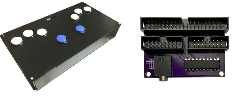
Figure 12: Controller button layout Here is a list of responsibilities per team member. Each
of us were tasked with implementing a subset of the main
subsystems in the full system.
We chose to make the controls hand-agnostic, so users
who prefer to translate with their left hand could do so. • Deanyone Su
We did this by using a 2x8 connector and designing the Primary Responsibilities
pinout to be reversible. Power and ground are rotationally
symmetric, and the other pins rotate to their left-handed – Game Logic
counterparts. – Graphics
Each button is wired with a 220Ω pullup resistor and
directly connected to its corresponding pin on the 2x8 con- • Eric Chen
nector. Ideally we would’ve used bigger resistors, but we Primary Responsibilities
had these on hand and the controller is still well below the
max current rating of the GPIO header. The FPGA will – Network Protocol
see a digital high or low value indicating the state of the • Alton Olson
button. Primary Responsibilities
The controller is housed in a sturdy laser-cut MDF box,
with cutouts for the buttons and the connector port. – Audio Synthesizer
While integrating the controllers, we discovered that – Game Controllers
cross-talk was occurring across the wiring into the FPGA.
As a result, on the release of any button on the controller,
any other pin(s) could spuriously assert. To mitigate this, 6.3 Budget
we would have preferred to do a hardware revision to run See Appendix B for our budget spreadsheet. This ta-
ground wires, but given the circumstances we had to de- ble includes all purchases made for this project, and there-
velop an on-chip mitigation strategy instead. First, we fore includes redundancies in the event that parts arrived
forced a global cooldown on all inputs, so after any input, nonfunctional. We came in quite far under the ceiling of
no inputs can occur for 15 cycles. This value is empiri- the budget provided. The remainder of the budget was in-
cally tested to filter out cross-talk across different inputs. tended to be used for revisions on our PCBs or replacement
Additionally, inputs must be asserted continuously for 63 parts. It turned out, though we did want to make revisions
cycles to register as a valid input. Again, this value was on our designs, we were unable to do so due to the COVID-
empirically tested with an additional safety margin on top. 19 impacts on the project and the course as a whole. We
In our testing we never saw a crosstalk input exceed a few ended up addressing the majority of our issues on-chip to
dozen cycles. 63 cycles at 50 MHz is too quick for anyone to compensate for the noise and crosstalk issues we saw across
reasonably detect while playing the game so while these do the network cables.
impact our metrics, it is not in a manner that is noticeable
to the user.
6.4 Risk Management
This project was planned to be built in parallel to re-
6 PROJECT MANAGEMENT duce risk of miscommunication. By building our compo-
nents as nearly stand-alone, we could have inflexible inter-
6.1 Schedule faces between subsystems, that were defined, while leaving
“internal” interfaces to be flexible and more amenable to
See Appendix A at the end of the report for our schedule modification. This is only possible with a limited number of
in the form of a color-coded Gantt chart. interfaces between each of subsystem so our responsibilities
Our first major milestone was to have a working pro- were allocated to reduce these intentionally.
totype by spring break. This included a working 40-line For parts, we ordered 50% to 100% more than needed
sprint mode, ability to generate audible music, and a hard- for our implementation. This reduced the risk and delays
ware testbench with data being transferred across FPGAs. associated with re-ordering parts. This was feasible due to18-500 Final Report - March 2, 2020 Page 14 of 18
the cheap cost of our parts, a lot of the components were of retro games, implementing Pong, Breakout, and Mas-
either provided by the school or low-cost. termind on FPGAs. Our original idea was largely based
Additionally, we sourced and ordered parts early. We around taking a retro game, building it onto an FPGA,
originally planned to do so to be able to begin prototyping and then taking it to the next level.
as early as possible and reduce the impact of discovering The Analogue Pocket is a consumer emulation product
that we needed more parts. It turns out this was a wise that is FPGA-based. Many open-source implementations
choice as many of our parts have some portion of their sup- can be found of Github/Gitlab and other nooks on the in-
ply chain in mainland China and the ongoing pandemic is ternet.
negatively impacting production in that part of the world.
With the impacts of COVID-19 on the course and our
project, there have been additional risks that need to be 8 SUMMARY
managed accordingly. With the closure of TechSpark and
campus as a whole, manufacturing and assembly became Our primary metric was response time relative to user
more difficult, especially since not all of us were located in input. This is achieved in our design since user inputs are
the same place. Akin to PCB printing, there exist laser- reflected on either the same or next frame sent to the VGA
cutting services that can accept provided design files to display. The current implementation is primarily limited
produce and ship out custom parts. We leveraged one of by the frame rate of the screen it is connected to and by
these to produce the laser-cut parts for the controller. This the clock speed of the FPGA. Being “frame-perfect” is a
introduces some additional cost to our project since we had nice phrase to use but it needs a refresh rate to provide
originally only accounted for material costs, but since we quantitative meaning. We define refresh rate using a stan-
were operating well under budget to begin with, this was a dard monitor with 60hz refresh rate. However, today there
minor concern. exist many monitors that can go to 75hz, 120hz, 144hz,
We had ordered PCBs prior to spring break, so we were 165hz, or even 240hz. Then, the term “frame-perfect” takes
able to get them shipped from campus before campus was on even stricter meaning. Therefore, our system’s metrics
entirely closed. With some assistance, we were also able could be further improved by driving a higher refresh rate,
to procure a soldering kit and some solder from campus as which provides information to the user at an even higher
well as the rest of our parts from the labs to be able to rate. Unfortunately, we are somewhat capped for the frame
assemble the boards in Pittsburgh. rate we could reasonably drive from our FPGA since higher
For remote development, we were able to have FPGAs resolutions and refresh rates require faster clock speeds to
shipped to us individually from campus. We have settled send across VGA. The fastest we could reasonably do at 50
on using the DE2-115 for its LE resources, seeing as the MHz is 72hz, 800x600 VGA output. To push faster than
area constraint imposed by the DE0-CV was difficult to this would require instantiating a faster pixel clock than
overcome. We had already been using a Github repository our native on-board crystal. This means locking a PLL to
for version control and to share code, so working remotely a desired frequency and passing data across clock domain
has had minimal impact on our ongoing RTL development. crossings. This is a reasonable course of action to take for
Minor delays incurred due to the situation are reflected in a future, long-term project.
the updated schedule. For this implementation, and the Tetris game, 72hz
frame rate is reasonable and our design stops here as a
demonstration of the improvement possible over a tradi-
7 RELATED WORK tional platform by using an FPGA implementation.
This project shares many aspects with emulation
projects. FPGAs are well suited for emulating retro game 8.1 Future Work
systems or late 20th-century hardware since clock speeds Looking to the future, there are a few things we would
and data rates of the era tend to be well below the ca- have liked to do but were unable to do so due to various
pabilities of modern FPGAs. Therefore, our work shares circumstances (primarily COVID-19) and time constraints.
facets with other works that attempt to emulate systems
such as the NES or Gameboy. Full emulators do exist, em- • PCB revisions. We designed the PCBs to route ex-
ulating the NES, SNES, and Gameboy (Original, Color, actly the number of wires we needed, plus a couple
and Advance). Our implementation is game-specific and more. This caused multiple data wires and the clock
is addressed at improving the experience in comparison to signal to be adjacent, which meant we had to build
modern systems, by addressing specific short-comings of several mechanisms into our on-chip designs to mit-
those modern implementations. igate the crosstalk generated. This is not ideal. We
It would be remiss to not mention the other emulation also built the controller circuitry on perfboard since
project in our own capstone group, Team C0’s GameBoi. it was a more flexible solution that could fit what-
They built a Gameboy Original cycle-accurate emulator ever dimensions the controller ended up being. In a
onto a DE10-Standard FPGA. We also credit inspiration future revision, we would interleave ground wires be-
for this project to the many 18240 Lab 5 implementations tween all the sensitive signals in the ribbon cable and18-500 Final Report - March 2, 2020 Page 15 of 18
also we would have a proper PCB fabricated for the needs to be some guarantee that the signal is glitch-
controller. less. In an early iteration of the network stack, the
sender and receiver modules on the slave board were
• Larger network. We originally had a plan for a design driven by a GPIO pin that received the clock signal
that could handle up to 4 players in a single multi- via the master board. This performed fine in intial
player session. Due to time constraints, we scaled this testing, but ended up causing some very interesting
down to two players only, which designing a network errors as crosstalk across the ribbon cable generated
for turned out to be challenging enough, especially near-random bitflips that were difficult to understand
when we down-scaled to the DE2-115 board with only and harder still to debug.
one GPIO header. However, given more time in the
future, it would be interesting to add more opponents
• Noise (and crosstalk) in wiring should be taken very
to the multiplayer mode. This introduces additional
seriously. We did not anticipate seeing these issues
complexity as new mechanisms, such as target selec-
and did not start to see the effects until we were well
tion, come into play.
into integration stages. Debugging an issue that only
occurred in our large design was very painful as the
8.2 Lessons Learned iteration cycles was very long. While debugging the
network, we saw flawless performance in our network-
Some lessons learned in the course of building this
only testbench, but the interference between wires
project:
caused significant issues once we had real data flying
• Start work early. Many aspects of what was being across the ribbon cables. Hardware revisions and bet-
built were not clear until we actually attempted to ter protocol design decisions would have been a huge
implement the module and realized there was a sig- help in mitigating the effects we were seeing. Trying
nificant challenge in the implementation details. to fix bad off-chip hardware with on-chip hardware
or protocols is very hard.
• Think about what is being implemented before imple-
menting it. Several rushed decisions ended up causing • In a similar vein, prioritize the testing of commu-
us significant efforts in re-writing modules, for exam- nication components outside of simulation, and the
ple: tools/environment necessary for doing so. This is
1. We originally decided to use 640x480 @ 60hz where we saw the most painful bugs that had to be
over VGA for our display but it turned our, upon debugged in the equivalent manner of throwing darts
closer inspection of the VGA standard, we could at a board. Initial network-only testing lacked the
do 800x600 @ 72hz over VGA. This afforded us ability to display the full extent of data being commu-
more space for our game on-screen and also en- nicated without graphics being integrated. The lack
abled us to achieve a lower I/O latency to the of a logic analyzer made it difficult to locate the exact
user, which we identified as our primary met- source and behavior of issues that arose when actu-
ric. However, it also meant we had to redefine ally running on the boards. Hex displays and LEDs
all the coordinates of major artifacts we had al- on the FPGA are a poor substitute for proper debug-
ready mapped out on-screen. ging tools. In hindsight, cross-board communication
should have been tested more robustly significantly
2. Using SRS, both I and O pieces do not have earlier, even if only with a prototype.
a center “tile”. Thinking that the center coor-
dinate was then arbitrary, we chose to use the
bottom right tile of the O piece as the origin for
that tile. It turns out, to spawn tiles correctly, References
it was a lot more elegant to have the bottom left
tile be the center, which meant rewriting parts [1] Alexander Atkishkin. 8-bit Monospace 6x6 Pixels Font.
of our rotation logic and rendering logic. Mar. 2020. url: https : / / previews . 123rf . com /
images/iunewind/iunewind1607/iunewind160700049/
• Write useful testbenches. A testbench should do more 60848823-8-bit-monospace-font-6x6-pixels-on-glyph-
than just check the correctness of a particular mod- vector-set-of-alphabet-numbers-and-symbols.jpg.
ule (though it should do at least that). A testbench
[2] Delayed Auto Shift. Sept. 2019. url: https://tetris.
should expect that a module will break and should
wiki/DAS.
also attempt to show the verifier what went wrong to
cause the fault. At the minimum, just display some [3] Texas Instruments. Dual 8-bit Multiplying Digital-to-
relevant information. Analog Converters. Mar. 2020. url: http://www.ti.
com/lit/ds/symlink/tlc7528.pdf.
• This should have been obvious from the classes we
all had taken in the past, but it is a bad idea to [4] William Nace. VGA: Mastermind. Apr. 2018. url: N/
use a clock signal directly from an I/O pin. There A.You can also read