Think Fast: A Tensor Streaming Processor (TSP) for Accelerating Deep Learning Workloads
←
→
Page content transcription
If your browser does not render page correctly, please read the page content below
2020 ACM/IEEE 47th Annual International Symposium on Computer Architecture (ISCA)

       Think Fast: A Tensor Streaming Processor (TSP)
          for Accelerating Deep Learning Workloads
   Dennis Abts, Jonathan Ross, Jonathan Sparling, Mark Wong-VanHaren, Max Baker, Tom Hawkins, Andrew Bell,
     John Thompson, Temesghen Kahsai, Garrin Kimmell, Jennifer Hwang, Rebekah Leslie-Hurd, Michael Bye,
         E.R. Creswick, Matthew Boyd, Mahitha Venigalla, Evan Laforge, Jon Purdy, Purushotham Kamath,
       Dinesh Maheshwari, Michael Beidler, Geert Rosseel, Omar Ahmad, Gleb Gagarin, Richard Czekalski,
                  Ashay Rane, Sahil Parmar, Jeff Werner, Jim Sproch, Adrian Macias, Brian Kurtz

                                                  Groq, Inc. · Mountain View, California

     Abstract—In this paper, we introduce the Tensor Streaming
  Processor (TSP) architecture, a functionally-sliced microarchitec-
  ture with memory units interleaved with vector and matrix deep
  learning functional units in order to take advantage of dataflow
  locality of deep learning operations. The TSP is built based on
  two key observations: (1) machine learning workloads exhibit
  abundant data parallelism, which can be readily mapped to
  tensors in hardware, and (2) a simple and deterministic processor
  with producer-consumer stream programming model enables
  precise reasoning and control of hardware components, achieving
  good performance and power efficiency. The TSP is designed
  to exploit parallelism inherent in machine-learning workloads
  including instruction-level, memory concurrency, data and model
  parallelism, while guaranteeing determinism by eliminating all
  reactive elements in the hardware (e.g. arbiters, and caches).
  Early ResNet50 image classification results demonstrate 20.4K
  processed images per second (IPS) with a batch-size of one—
  a 4× improvement compared to other modern GPUs and                         Fig. 1. Conventional 2D mesh of cores (a) reorganized into a functionally
  accelerators [44]. Our first ASIC implementation of the TSP                 sliced arrangement of tiles (b).
  architecture yields a computational density of more than 1
  TeraOp/s per square mm of silicon for its 25×29 mm 14nm chip               computers (WSC) [7], [11], [13]. These increasingly hetero-
  operating at a nominal clock frequency of 900 MHz. The TSP                 geneous systems have dozens of processing cores that vary
  demonstrates a novel hardware-software approach to achieve
  fast, yet predictable, performance on machine-learning workloads           widely in form and function, including GPUs, TPUs, FPGAs,
  within a desired power envelope.                                           and smart IO controllers for efficient remote direct memory
                                                                             access. Such efforts have largely focused on accelerating deep
                        I. I NTRODUCTION                                     neural network training and inference performance for a wide
     The world is increasingly turning to computationally-                   range of workloads: convolutional neural networks (CNNs)
  intensive deep learning algorithms to solve important problems             for recommendation algorithms, computer vision (CV) and
  in science, transportation, security, and beyond. These work-              image classification; recurrent neural networks (RNNs) for
  loads continue to grow both in size and complexity, presenting             natural language processing [20], [58]; and now attention and
  serious scalability, performance, and usability challenges for             transformer models [10], [55]. The increased computational
  traditional CPU and GPU architectures. Keeping pace with                   requirements of these models has been the catalyst for a
  this demand requires that we provision abundant on-chip                    resurgence of architectural innovation [21].
  ALUs and utilize them at near-peak performance throughout                     The demand for domain-specific architectures, as well as
  program execution. Unfortunately, hardware complexity of                   their widespread adoption into cloud computing ecosystems
  many microarchitectures makes it difficult to reason about                  [34], [48], provides a unique opportunity for novel microar-
  runtime stalls. Furthermore, while microarchitectural enhance-             chitectures targeting deep learning applications. A range of
  ments such as caches, branch predictors, and prefetchers help              innovative solutions are emerging—from Cerebras’ wafer-
  tremendously in improving performance, they do not bound                   scale integration [15] to more traditional chip multiprocessors
  worst-case performance.                                                    like GraphCore’s IPU [25]. Broadly speaking, all of these
     Over the last decade, data center operators have installed              efforts are focused on delivering more compute capability per
  many-core systems as a stalwart fixture in warehouse-scale                  floor tile in the data center. In other words, the focus is on

978-1-7281-4661-4/20/$31.00 ©2020 IEEE                                 145
DOI 10.1109/ISCA45697.2020.00023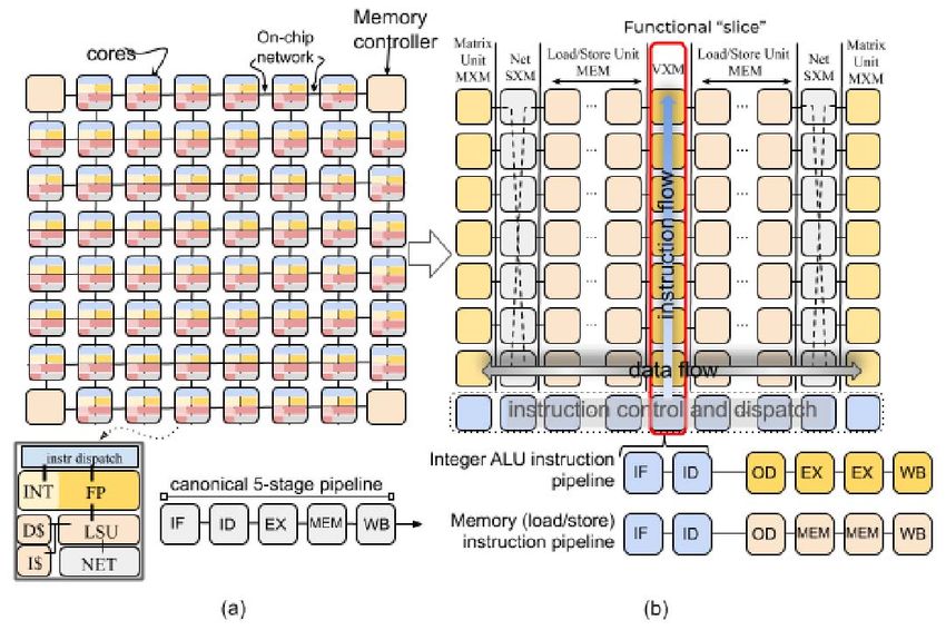
increasing computational density for a fixed power envelope. and Write but not Add or Mul, which are only in arithmetic
Our approach is based on rethinking conventional chip multi- functional slices (the VXM and MXM slices).
processor organization, resulting in a new architecture centered All of a slice’s tiles execute the same instruction stream
around the tensor abstraction, a Tensor Streaming Processor (SIMD), so we can factor out the common instruction decode
(TSP). The TSP uses a tiled microarchitecture that allows us to and dispatch logic into its own tile (ICU) and decompose
easily scale vector size to the underlying tensor shapes which the normal instruction execution pipeline into two areas:
they represent. Tensor computations are performed using a (i) instruction fetch, decode, and parceling and (ii) operand
streaming processing model where computational elements are read, execute, and writeback. This approach decouples the
arranged spatially by function to take advantage of dataflow memory subsystem [52] from the functional units retrieving
locality as tensors flow past. This novel approach enables us their operands and depositing results. Each functional slice
to achieve significantly better performance than the state of implements a 20-stage vector pipeline that spans the tiles of
the art, with initial Resnet50 image classification results of each slice, with each tile producing 16 elements of the 320-
20.4K sample images per second (IPS) using a batch-size of element maximum vector length. This organization naturally
one—a 4× improvement compared to other modern GPUs and decomposes instruction flow in the vertical dimension, and
accelerators [44]. In the remainder of this section, we discuss data flow in the horizontal dimension as it passes over different
the core architectural elements that set the TSP apart. function types. With this processor organization, instruction
execution is carried out by different tiles: instruction fetching
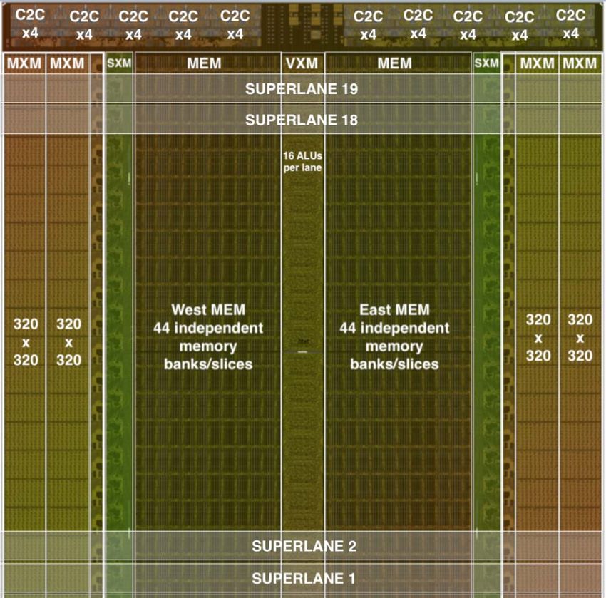
A. Functional slicing
and decoding in the ICU and operand decode, execution and
To understand the novelty of our approach, consider the writeback at each tile of functional slice as the (vertical
chip organization shown in Figure 1(a). In a conventional chip flowing) dispatched instruction intersects with the (horizontal
multiprocessor (CMP) [56] [12] each “tile” is an independent flowing) operand data on which it is operating.
core which is interconnected using the on-chip network to
exchange data between cores. Instruction execution is carried B. Parallel lanes and streams
out over several stages [46]: 1) instruction fetch (IF), 2) Data parallelism for each slice’s SIMD execution is pro-
instruction decode (ID), 3) execution on ALUs (EX), 4) vided via a programming abstraction called parallel lanes.
memory access (MEM), and 5) writeback (WB) to update the These parallel lanes correspond to elements of data vectors, an
results in the GPRs. In contrast from conventional multicore, abstraction common to many ML frameworks like TensorFlow
where each tile is a heterogeneous collection of functional [2]. In the TSP model, instructions flow Northward from
units but globally homogeneous, the TSP inverts that and the ICUs to the functional slices, while data (operands and
we have local functional homogeneity but chip-wide (global) results) flow East and West between functional slices. Any
heterogeneity. inter-lane data movement within a vector uses the on-chip
The TSP reorganizes the homogeneous two-dimensional network (SXM) slice.
mesh of cores in Figure 1(a) into the functionally sliced As shown in Figures 1 and 5, the on-chip network is im-
microarchitecture shown in Figure 1(b). In this approach, each plemented as X-dim mesh and Y-dim mesh of tiles with X-Y-
tile implements a specific function and is stacked vertically X dimension order routing. Each instruction specifies the first
into a “slice” in the Y-dimension of the 2D on-chip mesh. hop direction (East or West), so memory instruction semantics
We disaggregate the basic elements of a core in Figure 1(a) have both an address and a dataflow direction (Figure 2).
per their respective functions: instruction control and dispatch Streams are routed in the X-dimension through MEM, and
(ICU), memory (MEM), integer (INT) arithmetic, float point routed in the Y-dimension using the SXM’s permuter and lane-
(FPU) arithmetic, and network (NET) interface, as shown by shifters to move data elements vertically. The MEM and SXM
the slice labels at the top of Figure 1(b). Each row of the 2D provide deterministic routing [16] of stream data as it flows
on-chip mesh contains a cross section of all functional slices in the X and Y dimensions, respectively.
(see Figure 2). In this organization, each functional slice is Each element of a stream is 1-byte with larger data types
independently controlled by a sequence of instructions specific (e.g. int16, int32, and fp32) being constructed from several
to its on-chip role. For instance, the MEM slices support Read streams (2, 4, and 4 respectively). Multi-byte data types are
always naturally stream-aligned based on the size of the data
type. Data alignment is accomplished by the compiler. For
instance, int16 is aligned on a stream pair, and int32 is aligned
on a quad-stream (e.g. SG4 0 is stream 0-3, SG4 1 is streams
4-7, and so forth).
In a conventional load-store architecture the general-purpose
registers (GPRs) provide fast access to ALU operands and
storage of ALU outputs. As an example, consider a simple
sum of two N-element vectors, X and Y, to produce result Z,
as shown in Figure 3. In this example, a RISC core will loop
Fig. 2. The organization and dataflow within a row in the on-chip network. on four instructions to perform an element-wise addition: the
146
programmimg model, instruction set architecture (ISA)
                                                                                   and design tradeoffs for efficient operation at batch-size
                                                                                   of 1;
                                                                                  • we present early performance results on ResNet50 [27]
                                                                                   image classification model executing a sample image
                                                                                   query in less than 49μs, yielding 20.4K IPS of batch-size-
                                                                                   1 inference throughput, a 4-5× improvement compared
                                                                                   to Google’s TPU or Habana Lab’s GOYA chips; and
                                                                                  • we provide a detailed discussion of architecture trade-
Fig. 3. Conventional RISC execution contrasted with producer-consumer
streams in the TSP.                                                                offs for accelerating machine learning workloads more
Add R1,R2,R3 would first need a LOAD R1,X and a LOAD                                generally, and lessons learned from mapping ResNet50
R2,Y to move the operands into the GPRs, and the result                            v2 image classification model to the TSP hardware.
in R3 must be written back to main memory with STORE                                           II. A RCHITECTURE OVERVIEW
R3,Z. With the TSP architecture, functional slices interact                      The tensor stream processor architecture makes several de-
with streams of data in a producer-consumer fashion. That                     liberate tradeoffs on the hardware-software interface, pushing
is, they consume operands from streams and produce results                    the complexities associated with scheduling into the compiler.
onto a (possibly different) stream, similar to an assembly line               Specifically, it falls on the compiler to precisely schedule
operator (functional slice) and conveyor belt (stream).                       instructions so as to use the hardware correctly and efficiently.
   Conceptually, the functional slices are fixed and data is
                                                                              At times this may involve selecting one of several means by
flowing across their processing elements as shown in Figure
                                                                              which an algorithm or meta-operation may be realized on
2. As the data flows through the slice, each functional unit can
                                                                              the hardware. Removing the control complexity of dynamic
optionally intercept the data operands and compute a result (if
                                                                              instruction scheduling for multi-issue execution units allows
its a processing element like an ALU), or move data between
                                                                              the instruction control unit (ICU) to be relatively small,
lanes on the network if its a switching element.
                                                                              accounting for less the 3% of the area. The compiler has access
   Streams provide a programming abstraction and are
                                                                              to the following architecturally-visible state:
a conduit through which data flows between functional
                                                                                  • 320-lane programming abstraction overlaid on the
slices. Unlike GPRs, the functional slices operate on streams of
                                                                                   TSP block diagram (Figure 5) where each tile in the
parallel data flowing East or West across chip. The horizontally
                                                                                   on-chip mesh operates on 16-lanes in a SIMD manner.
flowing streams carrying operands intercept the vertically
                                                                                   We refer to this 16-lane unit as a “superlane” which
(Northward) flowing instructions (Figure 2) to perform a com-
                                                                                   is a cross-section of all the functional slices on the
putation on a functional slice. The compiler precisely tracks
                                                                                   chip and the minimum granularity of computation. As
the chip’s architectural state and uses that knowledge to ensure
                                                                                   such, a superlane represents the architecture’s minimum
that instructions correctly intercept its stream operand(s).
                                                                                   vector length, minVL, of 16 elements. Likewise, the
   Streams are implemented in hardware by a chip-wide
                                                                                   vertical composition of 20 tiles to form a functional slice
streaming register file (SR). They are architecturally-visible
                                                                                   (Figure 5) produces a maximum vector length, maxVL,
and transport operands and results between slices. A common
                                                                                   of 20×16=320 elements.
software pattern involves reading operand data from one or
                                                                                  • 144 independent instruction queues (ICUs) on-chip,
more MEM slices that is then subsequently consumed and
                                                                                   each can issue one or more instructions per cycle and
operated on by a downstream arithmetic slice. The results of
                                                                                   the compiler has explicit control of the program order in
the operation are then produced onto another stream such that
                                                                                   each instruction queue.
they can be written back to memory. For example, a Z=X+Y
                                                                                  • 64 logical streams per lane for moving operands or
operation might require four instructions: Read S1,X and
                                                                                   results on-chip with 32 streams Eastward, and 32 streams
Read S2,Y are executed on two MEM slices and directed
                                                                                   Westward as shown in Figure 2.
inward toward an INT slice to perform the Add S1,S2,S3.
                                                                                  • 220 MiBytes of globally shared SRAM that delivers
Lastly, the result is stored back to memory via a Write
                                                                                   32 bytes per lane of stream bandwidth and low-latency
S3,Z. The streams represent a collection of N -elements,
                                                                                   access to model parameters. For example, the MEM can
operated upon in a SIMD manner by each functional slice.
                                                                                   read and MXM can install 400K weights into all four
C. Paper organization                                                              320×320 arrays in less than 40 cycles including SRAM
   The remainder of this paper describes the microarchitec-                        and on-chip network transit delay.
ture of the Groq tensor streaming processor (TSP) with the                       Streams are designated by both an identifier 0..31 and
following contributions:                                                      direction, for instance, in(28) designates stream 28 inward, and
    • we introduce functional-sliced tile microarchitecture and               out(24) is stream 24 toward the outward edge of the chip1 .
     the stream programming abstraction built upon it;                          1 We use both inward (toward the chip bisection) and outward (toward
    • we describe our first implementation of the TSP in 14nm                  the outward edge of the chip) as well as cardinal directions Eastward and
     ASIC technology, memory system and functional units,                     Westward as shown in Figures 2 and 4.

                                                                        147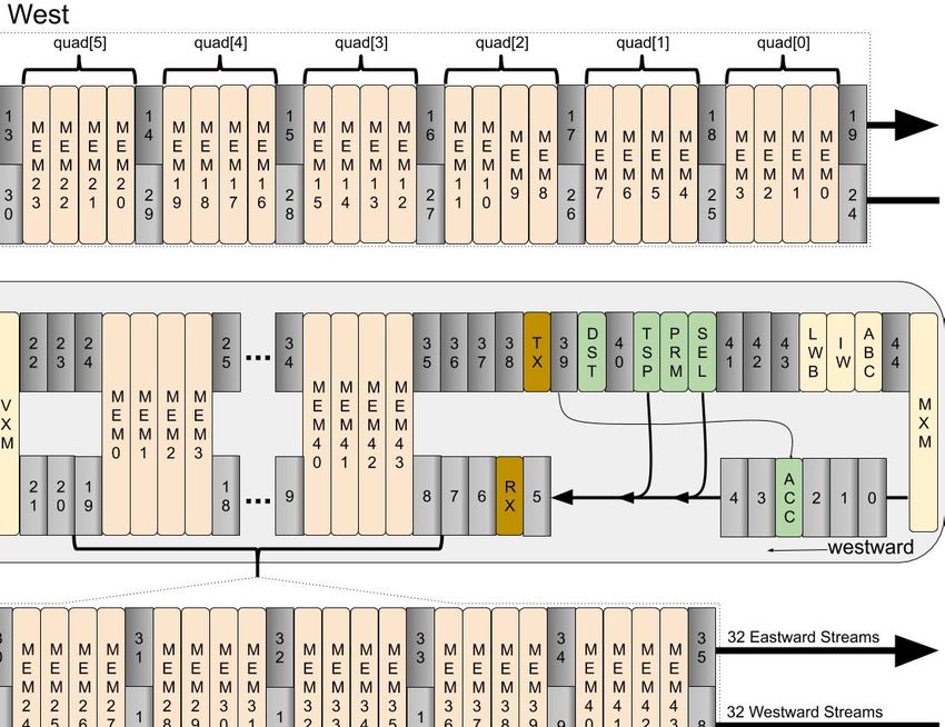
Fig. 4. Stream registers are numbered to show their locations between the functional slices within a superlane.

The components of a superlane are organized spatially as                       toward the functional slice intending to operate on them.
shown in Figure 2. The TSP’s instruction set architecture (ISA)                  1) The instruction control unit (ICU) provides explicit
defines instructions spanning five different functional areas.                        instruction fetching with IFetch, and inter-slice syn-
The partitioned global address space (PGAS [6]) presented                           chronization using Sync and Notify instructions to
by the memory (MEM) slices provides memory semantics                                perform a chip-wide barrier synchronization among par-
for vectors to be addressed from SRAM and loaded into                               ticipating functional slices. A repeated-NOP (no-op) in-
an architecturally-visible stream with a direction of dataflow                       struction allows for precise cycle-by-cycle control of
                                                                                    inter-instruction delay; for example, the compiler has
                                                                                    cycle-accurate control when scheduling two operations A
                                                                                    and B using an intervening NOP so that N cycles separate
                                                                                    them OpA NOP(N ) OpB.
                                                                                 2) A vector execution module (VXM) consists of a 4×4
                                                                                    mesh of ALUs in each lane for point-wise arithmetic
                                                                                    operations.
                                                                                 3) The matrix execution module (MXM) consists of four
                                                                                    (4) independent 2D MACC (multiply-accumulate) arrays
                                                                                    that operate on int8 or fp16 data types.
                                                                                 4) On chip data movement uses the switch execution mod-
                                                                                    ule (SXM) for intra-superlane and inter-lane switching by
                                                                                    rearranging elements of vectors. The SXM is analogous
                                                                                    to the NET interface to communicate between cores in
                                                                                    Figure 1. Together the MEM and SXM work in tandem
                                                                                    to form the X-Y dimensions of the on-chip network.
                                                                                 5) The East and West hemisphere of on-chip memory
                                                                                    module (MEM) is composed of 44 parallel slices of
                                                                                    SRAM and provides the memory concurrency necessary
                                                                                    to fully utilize the 32 streams in each direction. Each
                                                                                    slice provides 13-bits of physical addressing of 16-byte
                                                                                    memory words, each byte maps to a lane, for a total of
                                                                                    220 MiBytes of on-chip SRAM.
                                                                                 6) Chip-to-chip (C2C) modules provide Send and
                                                                                    Receive primitives for exchanging 320-byte vectors
                                                                                    between a pair of chips. The first TSP implementation
                                                                                    (Figure 5) has a total of sixteen (16) ×4 links operat-
   Fig. 5. Die photo of 14nm ASIC implementation of the Groq TSP.                   ing at 30 Gbps each for a total off-chip bandwidth of

                                                                         148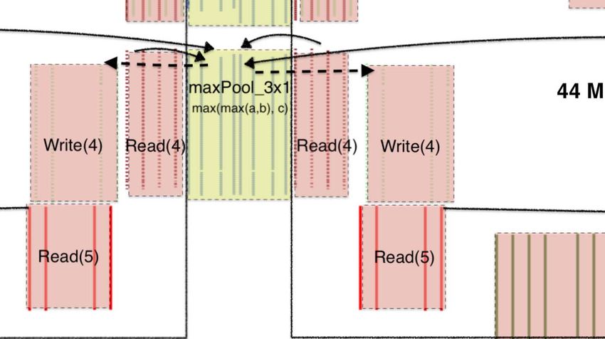
Function        Instruction     Description
                         NOP N         No-operation, can be repeated N times to delay by N cycles
                         Ifetch        Fetch instructions from streams or local memory
                          Sync         Parks at the head of the instruction dispatch queue to await barrier notification
          ICU
                         Notify        Releases the pending barrier operations causing instruction flow to resume
                         Config        Configure low-power mode
                      Repeat n, d      Repeat the previous instruction n times, with d cycles between iterations
                        Read a,s       Load vector at address a onto stream s
                       Write a,s       Store stream s register contents into main memory address a
         MEM
                    Gather s, map      Indirectly read addresses pointed to by map putting onto stream s
                   Scatter s, map      Indirectly store stream s into address in the map stream
                     unary operation   z = op x point-wise operation on 1 operand, x, producing 1 result, z (eg. mask, negate)
                    binary operation   z = x op y point-wise operations with 2 operands x and y producing 1 result, z (e.g. add, mul, sub)
                    type conversions   Converting fixed point to floating point, and vice versa
         VXM              ReLU         Rectified linear unit activation function max(0,x)
                          TanH         Hyperbolic tangent - activation function
                           Exp         exponentiation ex
                         RSqrt         Reciprocal square root
                            LW         Load weights (LW) from streams to weight buffer
                            IW         Install weights (IW) from streams or LW buffer into the 320×320 array
         MXM
                           ABC         Activation buffer control (ABC) to initiate and coordinate arriving activations
                           ACC         Accumulate (ACC) either INT32 or FP32 result from MXM
                  Shift up/down N      Lane-shift streams up/down by N lanes, and Select between North/South shifted vectors
                                                                      map
                     Permute map       Bijective permute 320 inputs−−−→outputs
         SXM      Distribute map       Rearrange or replicate data within a superlane (16 lanes)
                    Rotate stream      Rotate n × n input data to generate n2 output streams with all possible rotations (n=3 or n=4)
                  Transpose sg16       Transpose 16×16 elements producing 16 output streams with rows and columns interchanged
                         Deskew        Manage skew across plesiochronous links
         C2C              Send         Send a 320-byte vector
                        Receive        Receive a 320-byte vector, emplacing it in main memory

                                                              TABLE I
                                         S UMMARY OF INSTRUCTIONS FOR EACH FUNCTIONAL SLICE .

     16 ×4 ×30Gb/s ×2 directions = 3.84 Tb/s of off-chip pin              direction: eastward, or westward. Once the vector is read
     bandwidth that can be flexibly partitioned to support high-           into a stream register it is a stream and is “flowing” in the
     radix [37] [49] [3] interconnection networks of TSPs for             given direction in the following sense: Given spatially-adjacent
     large-scale systems. The host interface for PCIe Gen4 is             functional slices at coordinates x0 , x1 , x2 (where the spatial
     also handled in this module. It provides a lightweight               coordinate increases in the direction of flow), then at a given
     DMA engine to emplace a model onto the TSP memory,                   time ti , the vector representing stream s1 at slice x1 can be
     and provides an entry point for bootstrapping the model              accessed as operands by that slice. Similarly, the slices at x0
     execution. It also provides a general mechanism for                  and x2 will have access to different stream values for the
     passing interrupts to the host, which may be necessary               same stream register. In the following cycle ti+1 , the value
     in the event we observe a multi-bit memory error, for                s1 either propagated to the functional slice at x2 , or else it
     example.                                                             is overwritten with a result r1 produced by the slice at x1 at
   A sequence of instructions performed on different functional           cycle t. Similarly, the stream value s0 that was present to be
slices can be chained to create more complex actions without              consumed by the functional unit at coordinate x0 at time ti will
the need to writeback intermediate results to memory. This                be (absent x0 overwriting the value at time ti ) available in the
allows us to efficiently process streams at full bandwidth and             next cycle ti+1 to the slice at x1 . Stream operands are steered
lowest latency.                                                           toward the slice that is consuming them and producing a result
                                                                          stream. Streams are constantly flowing across the chip, serving
A. Parallel streams programming model
                                                                          as the means by which slices communicate with one another.
   Machine learning algorithms typically operate on vectors               Figure 4 provides a graphical depiction of the interleaving of
with coefficients of a specified data type (eg. int8, fp16, etc).           functional units and stream registers that combine to support
We may interpret these vectors as an abstraction over the                 this programming model.
underlying data, whose elements can be processed by the same
operation in a SIMD manner. The TSP operates on vectors,                  B. Memory model
sometimes organized into rank-2 tensors, and relies on the                   The on-chip memory supplies operands for each functional
graph-lowering compiler to transform higher rank tensors into             slice by reading an address from a memory (MEM) slice,
rank-2 tensors over hardware-supported data types.                        denoted MEMi . Memory is partitioned into two hemispheres
   The TSP’s programming model is a producer-consumer                     (Figure 5), each having 44 slices numbered 0 to 43 with
model where each functional slice acts as a consumer and                  slice MEM0 closest to the VXM and MEM43 nearest to the
a producer of one or more streams. When a vector is read                  SXM. Each MEM slice comprises 20 tiles, arranged in a
from main memory it is given a stream identifier (0..31) and               vertical stack, yielding a 2.5 Mibyte per-slice capacity, or

                                                                    149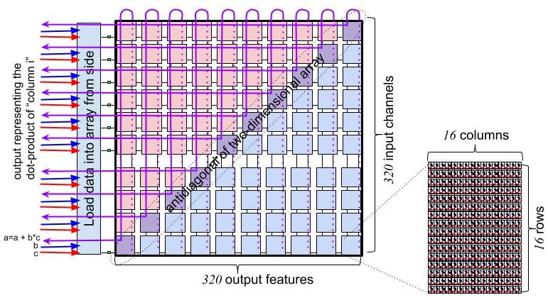
220 MiBytes for all 88 slices on-chip. The 88 slices provide              super lane of operand vectors. This process continues cycle-
the needed memory concurrency to supply 32 operands per                   by-cycle until it has traversed all 20 tiles in the slice. The
lane, every cycle. Slices of memory are partitioned into 16-              combination of vertical instruction pipelining described above,
byte words, each word spread across a superlane, and each                 along with the need for operands and instructions to coincide
byte of each word occupying a lane of an input channel                    at a precise time, results in a spatial “stagger” of SIMD
or an output feature. That is, byte 0 is lane0, byte 1 is                 operand and result data as depicted in Figure 6. As shown,
lane1, and so forth. Each tile produces a ×16 portion of the              a single 320-byte vector, represented as 20 black squares, are
vector, which is concatenated with the 16 elements from the               moving eastward along a stream. The data for successive 16-
adjacent tile beneath. Instructions execute in a cycle-by-cycle           element superlanes are lagging by 1 cycle to accommodate
staggered manner across all 20 tiles in the slice; instructions           the pipelined execution of an MXM instruction issued to the
flow Northward over the span of 20 cycles visiting each tile               southern-most tile depicted at time t1 .
in the slice.
                                                                          D. Error handling and reliability
   For the sake of exposition, assume a 1 GHz operating
frequency of the core clock. The stream register bandwidth, B,               Large scale deployments within warehouse-scale computers
exported by each MEM interface on the East and West edge                  [11] require hardware-based error correction when possible to
of each MEM hemisphere is capable of keeping the functional               be resilient in the face of transient errors. The error correcting
units adequately fed with data operands in order to saturate the          code (ECC) used to protect vectors in SRAM memory is also
peak arithmetic capacity of the functional units. The stream              used as they flow on the stream registers on-chip. Since the
registers provide a combined capacity of 20 TiB/s of read                 memory system is highly banked and replicated, we want to
(operand) and write (result) bandwidth, as shown in Eq. 1.                avoid replicating the XOR-tree for computing ECC across a
                                                                          wide, 128-bit, memory word. Instead, we take advantage of the
                        bytes                                             producer-consumer nature of the stream programming model
 B = 2 directions × 32        × 320 lanes = 20 TiB/s (1)
                        lane                                              and generate ECC check bits only at the producer and they are
Since the SRAM banks are shuttling data between the stream                stored alongside the 128-bit memory word as 9-bit ECC, 137-
registers and SRAM cells, the SRAM bandwidth, M , must                    bits in total. The ECC scheme implements SECDED (single-
exceed the stream bandwidth B. The SRAM bandwidth of                      error correction with double-error detection) to allow us to
on-chip memory is given in Equation 2.                                    tolerate a single-bit error in the memory word or anywhere
                    slices    banks        bytes                          along the streaming data path. When a functional slice is going
M = 2 hem × 44             ×2        × 320        = 55 TiB/s              to operate on a stream, ie. consume a stream, it will check the
                     hem       slice        cycle
                                                             (2)          ECC bits to ensure data integrity before operating on it. This
on-chip memory bandwidth, or 27.5 TiB/s of SRAM band-                     mechanism covers both the SRAM soft errors, any datapath
width in each hemisphere.                                                 soft errors that might arise in the stream registers.
   Instruction fetching (further described in Section III-A3)                Any soft error upsets (SEUs) on operands or instruction text
consumes a maximum SRAM bandwidth of 144×16, or 2.25                      are automatically corrected and recorded in a control and status
TiB/s of maximum instruction fetch bandwidth. Each MEM                    register (CSR) for an error handler to interrogate later. These
hemisphere exports 20 TiB/s of stream bandwidth from its                  transient soft errors and automatic corrections are an early sign
27.5 TiB/s of SRAM bandwidth which must also satisfy                      of wearout and often used as a proxy for identifying marginal
the maximum instruction issue rate of 2.25 TiB/s across all               chips in large-scale systems.
functional slices. With 27.5 TiB/s of SRAM bandwidth and                  E. Chaining functional slices
2.25 TiB/s of instruction fetch bandwidth, this still leaves 25              Each functional slice has a predefined set of instructions
TiB/s of SRAM bandwidth from which to service 20 TiB/s of                 (eg Read, Write, Add, Mul, etc) that define its supported
stream register bandwidth for operands and results.                       operations. Furthermore, functional slices consume operands
C. Staggered instruction execution                                        from and produce results to streams. A more complex se-
                                                                          quence of operations, a microprogram, is composed of one
   In the TSP programming model, an instruction is issued
on a functional slice at a given compiler-scheduled time t,
and executes as a SIMD operation on stream-supplied operand
vectors (of up to 320-elements), producing vectors of the same
length on result streams. At the micro-architectural level, the
320-element SIMD instruction is pipelined across the vertical
stack of tiles in the slice. That is, at the scheduled time
t the instruction will be issued to the bottom-most tile of
the slice, (corresponding to the first 16-element superlane of
operand/result vectors). In the subsequent cycle, the instruction
will be propagated to the next tile northward in the slice,
which in turn executes the instruction on the next 16-element              Fig. 6. Staggered instruction execution and dataflow within a superlane.

                                                                    150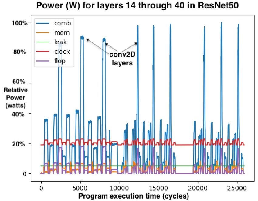
or more slices coordinating in a producer-consumer manner               The parameters are necessary to track the exact spatial re-
to create one or more output streams. This is accomplished              lationship between instructions and operands. Conceptually,
by logically “chaining” multiple slices together to consume             the compiler is solving a two-dimensional scheduling of in-
input data from up-stream slices, operate on that data to               structions and data in both time and space (ie. stream register
produce a new result stream, where it later can be consumed             location on-chip as shown in Figure 4). The execution time
by a down-stream slice in a similar manner. In general, each            of an instruction includes the instruction functional delay,
functional slice can choose the direction of its result stream,         and stream propagation (transit) delay to get from stream
so that streams can be logically “turned around” (ie. reverse           register location i (SRi ) to j (SRj ), as shown in the superlane
their direction of flow from East-to-West, or vice versa) at             dataflow in Figure 4.
any slice. With this cooperative producer-consumer model
operating on data streams we can compose more elaborate                                      T = N + df unc + δ(j, i)                   (4)
operations by chaining together different functional slices as          In Equation 4 the time, T , executing an instruction where N
shown in Equation 3 below, where a composite function, F ,              is the number of tiles in the functional slice, and df unc is
is an amalgam of several functional slices chained together.            the functional delay of the instruction being executed (cycles)
     F (x, y, z) = MEM(x) → SXM(y) → MXM(z)                 (3)         for the output stream to appear on the SRi (stream register
                                                                        at location i in Figure 4) en route to the consumer at SRj .
This dataflow composition allows us to exploit “data flow                 The transit delay, δ(j, i) is the distance (in cycles) between
locality” by passing the same data across multiple functional           SRj and SRi . The TSP programming model relies on two
slices which can optionally operate on the data to produce              critical elements: (1) deterministic data paths in hardware,
some output stream. The output from one functional slice                and (2) exposing temporal information about an instruction’s
can be used as the input to another slice allowing for logical          execution latency through the ISA, the compiler’s back-end
chaining of operations through a common stream register.                can precisely track the position and time-of-use of any stream
                                                                        on-chip. Exposing this additional temporal information across
F. Scalable vectors
                                                                        the static-dynamic interface [43] giving rise to “software-
   The underlying data type supported by the TSP hardware               defined hardware.”
is a vector. The number of elements in each vector can vary                The remainder of this section provides an summary of
from 16 elements, one superlane, all the way to 320 elements            the different instructions available on each functional slice.
using all 20 superlanes on-chip. That is, the minimum vector            We discuss each functional slice type and give examples in
length, or minVL, is 16 bytes and maxVL is a 320 byte-sized             assembly language.
element array. A maxVL of 320 bytes is comparatively long
compared to typical SIMD extensions to x86 (e.g AVX512b                 A. Instruction control unit (ICU)
[31]). Because the vector length (VL) can vary from 16 to                  The instructions in the instruction control unit (ICU) are
320 elements, we provide instructions to configure each tile             common to all functional slices. As such, they contain com-
for a low-power mode to effectively power-down any unused               mon instructions like NOP and Repeat, and synchronization
superlane (row of the mesh) and reduce the power consumed.              primitives Sync and Notify to allow the independent func-
This scalable vector approach allows us to grow the VL from             tional slices to be initially synchronized so the compiler can
16 to 320 bytes in 16-lane steps, powering-down the unused              reason about instruction execution times and allow cooperative
tiles, yielding a more energy-proportional [14] system.                 parallelism among the functional slices on-chip.
                   III. I NSTRUCTION SET
                                                                         1   import groq.api as g
  The TSP’s instruction set architecture (ISA) exposes tempo-            2   x = g.random_tensor(shape=[1024, 320],
ral information about each instruction to allow the compiler             3                        dtype=g.Int8)
                                                                         4   y = g.random_tensor(shape=[1024, 320],
precise control of each instruction’s dispatch time. We aug-             5                        dtype=g.Int8)
ment each instruction with the following temporal parameters:            6   x_strm = x.read(stream=’S_0’)
    • df unc functional delay — each instruction requires 1              7   y_strm = y.read(stream=’S_4’)
                                                                         8   z = g.add(x_strm, y_strm, stream=’S_0’)
     or more cycles to produce its stream output. The df unc             9   out_addrs = g.malloc([1024, 320])
     timing parameter allows the compiler to reason about               10   z.write(out_addrs)
     when the output of an instruction will be available on
                                                                                   Listing 1. Streaming Add from example in Figure 3.
     the architecturally-visible stream registers.
    • dskew instruction-operand skew — the timing rela-                   1) No-op: The compiler uses explicit NOPs to provide tem-
     tionship between the instruction dispatch time relative            poral separation between two instructions in program order. A
     to when its stream operands are required. The dskew                NOP has a repeat count 16-bit field which allows 1 NOP to
     parameter on each instruction informs the compiler how             wait from 1 ns up to 65 μs for a 1GHz clock. The compiler
     to schedule the operand arrival times with the instruction         uses NOP instructions to control the relative timing of the
     dispatch time in order to get them to properly intersect           functional slices and the data on which they operate. The
     in time and space.                                                 repeated NOP is implemented in the ICU’s tile and common to

                                                                  151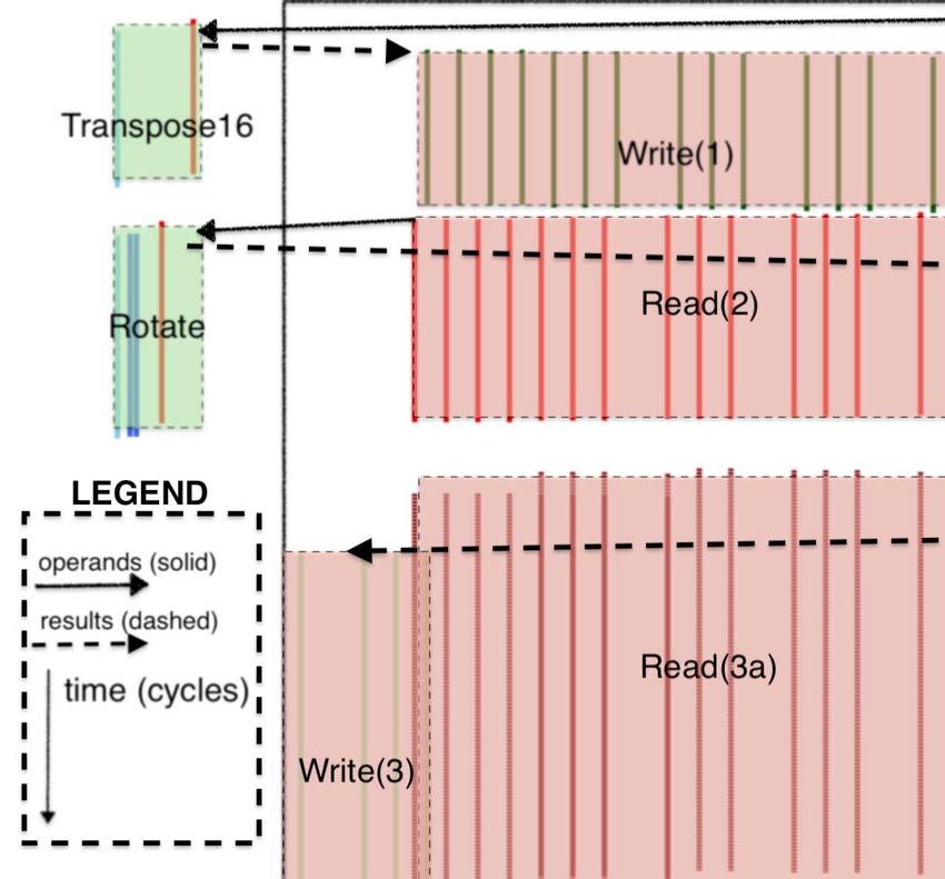
all functional slices. The NOP allows the slice to turn off the
clock enables when NOP-ing for anything longer than a few
cycles. While NOP is likely the most common instruction, it
is not programmer-visible in as much as the compiler inserts
them implicitly.
   2) Synchronization: Each functional slice is independent,
however, the compiler keeps track of a logical program time.
Conceptually it is similar to a program counter in a con-
ventional CPU, except the compiler tracks the state of 144
independent program queues on a cycle-by-cycle basis. So at
logical time t the compiler knows the state of each IQ on
the chip. We use a NOP instruction to coordinate the temporal            Fig. 7. The MXM block diagram showing activations and weights being
relationship between instructions in the same IQ, or between             loaded at the side of the array, and INT32 or FP32 results flow back from
instructions in different IQs. In addition to repeated-NOPs              the inside edge.
we must provide a higher-level synchronization across all                memory concurrency—88 slices each with 2 banks—to read
functional slices on the chip in order to reason about program           operands to or store results from streams.
correctness. That is the role of the Sync and Notify in-                    Each MEM slice supports both direct and stream-indirect
structions. They provide a barrier synchronization mechanism             addressing modes. Read and write use direct addressing,
across all 144 independent queues on the chip. One IQ is                 since the address is fully specified in the instruction itself.
designated as the notifier and it issues a Notify instruction             Indirect addressing uses the contents of a stream, s, to specify
while all other IQs are parked on a Sync instruction — receipt           an address map for a gather or scatter. With indirect
of the Notify is broadcast to all the IQs to satisfy the pending         addressing, the physical address comes from the stream value,
Sync and begin processing instructions again.                            providing a layer of indirection in the memory referencing.
   This barrier synchronization is only required once after the
chip resets. However, in practice, we start each program with            C. Vector (VXM) processor
a set of “preamble” instructions which configure each tile then              Each superlane implements a 4x4 mesh of vector ALUs
perform a Sync to ensure that all functional slices are aligned          capable of doing ×16-SIMD computations — 16 vector ALUs
to the same logical time. A chip-wide barrier synchronization            per lane. Each of the ALU’s 32-bit input operands are orga-
can be accomplished in 35 clock cycles, from the time the                nized along naturally aligned quad-stream group (SG4). The
Notify is issued to the time the Sync is satisfied and retired            vector ALUs do not produce condition codes or status flags
to allow subsequent instructions to flow. After this compulsory           from the last instruction; they are stateless. Instead, the VXM
barrier synchronization, the functional slices can compute and           provides both saturating and modulo variants (add_sat,
communicate results in a synchronization-free manner through             add_mod and mul_sat, mul_mod) for addition and mul-
the stream registers and reason about program correctness                tiplication, which allows differing semantics for handling
using a simple timing model (Figure 4) of the chip.                      arithmetic exceptions. The TSP supports chaining together two
   3) Instruction fetching: The Ifetch instruction has a                 or more vector ALUs within each lane, allowing multiple
single stream operand which carries the text of the instructions         ALU operations to be performed without committing the
in their program order, filling the IQ with 640-bytes (a pair             intermediate results to main memory, saving a write and
of 320-byte vectors) of instructions. All functional slices              subsequent read of each intermediate result. This allows for
can fetch instructions simultaneously with normal instruction            efficient parallel implementations of algorithms for batch nor-
execution. The compiler performs omniscient prefetching of               malization, quantization, or more complex activation functions
the program’s text to keep all 144 IQs busy on each cycle by             like leaky ReLU activation function, for instance.
inserting Ifetch instructions into every slices’ instruction
stream. It is imperative that IQs never go empty so that a               D. Matrix execution module (MXM)
precise notion of “logical time” is maintained across the chip.             The matrix execution module (MXM) provides four (4) in-
                                                                         dependent 320×320 (Figure 7) planes of multiply-accumulate
B. Memory (MEM)                                                          (MACC) units. Each 320×320 plane is comprised of 20
   The memory (MEM) slices provide the programming ab-                   16×16 supercells that produce a partial-sum each cycle and
straction of a partitioned global shared address space with              pass it to the adjacent tile for use in its computation. It requires
the address space laid out uniformly across the 88 slices.               16 streams each with 16 bytes to install 256 8-bit weights
Each MEM slice contains pseudo-dual-port SRAMs that are                  (IW) in each supercell on every cycle. Using all 32 streams
capable of servicing a pair of read and write requests                   in each direction allows us to emplace weights in both MXM
simultaneously assuming they are not targeting the same bank.            planes simultaneously on both MXM hemispheres, loading all
As such, we expose the bank bit so that the compiler can                 409,600 weights on-chip in less than 40 cycles. With weights
manage the underlying SRAM efficiently and appropriately.                 installed, every cycle the MXM can generate a new int32
This allows the compiler to take advantage of up to 176-way              dot-product of input activations with installed weights. The

                                                                   152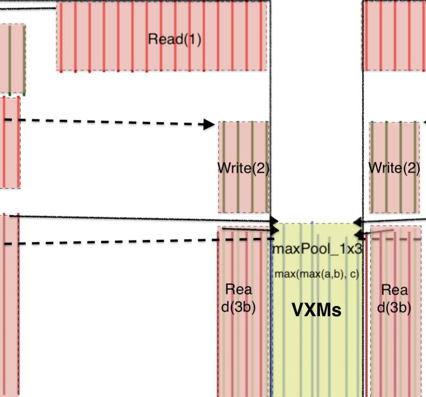
different MEM slices where they are now addressable. There
                                                                              are two instances of the SXM on-chip, one in each hemisphere
                                                                              (Figure 5). Each can issue two (2) transpose instructions,
                                                                              yielding a maximum of four (4) simultaneous transpose
                                                                              16x16 operations.

                                                                                                     IV. R ES N ET 50
                                                                                 In this section we describe our early results and lessons-
                                                                              learned from implementing ResNet50 [27], a popular image
                                                                              classification model, on the TSP hardware. In the process
                                                                              of bringing up new hardware, the software stack is critical
                                                                              for mapping the underlying tensor operations to the TSP’s
Fig. 8. The SXM provides a combination of North (up) and South (down)         instruction set that implements them. The compiler is also
shifting operations which can be combined using the select.
                                                                              responsible for memory management of tensors (weights and
                                                                              activations) and program text which describes the model itself.
features output from the MXM can be accumulated using the                     The MEM system provides the compiler with a flat, globally
accumulators on each int32 or fp32 output stream.                             shared address space, with 220 Mibytes of total capacity. As a
   The MXM supports numerics for both 8-bit integer, and                      matter of policy, the compiler reserves several MEM slices to
16-bit floating point by using two 320×320 byte-planes in                      serve as “instruction dispatch” slices where the machine-coded
tandem for 16-bit floating point results. The 320-element sum                  instructions are stored and supplied on streams to service
is produced for each output with only a single rounding step                  Ifetch instructions on different functional slices where the
at the end to convert to int32 or fp32 results.                               instructions will eventually be executed.
                                                                                 As a broad objective, the model implementation seeks to
E. Switch execution module (SXM)                                              maximize functional slice utilization, and minimize latency.
   The switch execution module (SXM) contains several func-                   This means we want to take advantage of streaming operands
tions for transposition, permutation, shifting and rotation of                into the MXMs and VXMs as much as possible. The four
data elements. Collectively, these operations are used for per-               (4) 320×320 MXM planes are used for matrix multiply
forming tensor reshape operations common to ML workloads,                     operations. The 16 vector ALUs in each lane are tasked with
and fulfill the functionality of the NET slice in Figure 1. Data               requantizing the int32 outputs from the MXM to produce
movement on-chip is carried out by routing data in two dimen-                 int8 results which are streamed through an activation function
sions: horizontally propagating streams in the X-dimension                    ReLU [8]. From the perspective of both performance and
shuttling between SRAM and functional units within each                       power, when possible we want to chain the results from one
superlane, and vertically in the Y-dimension where the SXM                    functional slice (eg. MXM) to the input of another functional
is used to move streams in the North-South directions. The                    slice (eg. VXM) eliminating the read and write operations
SXM provides two sets of lane shifters that execute shift                     to store the intermediate results to MEM. Figure 10 shows a
instructions (Figure 8) both North and South. The lane-shifters               plot of power consumption as the program executes, layer by
are usually allocated in pairs since we typically shift a vector              layer. The spikes in the power correspond to cycles where we
up or down and select which elements we want from either                      perform four (4) simultaneous conv2d operations in a regime
(i) North-shifted, (ii) South-shifted, or (iii) unshifted data                where we saturate the TSP’s arithmetic throughput.
elements, as shown in more detail in Figure 8. In addition,
                                                                              A. Explicitly managing memory
the SXM provides a permute instruction which employs
a programmed bijection to remap the 320 lanes on a set of                        To maximize stream concurrency, the compiler allocates
similarly indexed streams, one per superlane.                                 memory for a tensor’s concurrent stream operands into sepa-
   The distributor slice within the SXM is used to arbitrarily                rate MEM slices — as streams propagate through the MEM
remap the 16 lanes within each superlane. As streams pass                     system they “pick up” operands from the MEM slices en route
through the distributor, they can be remapped at full band-                   to the MXM. This fine-grain memory management required
width, or zero-fill any or all of the 16 elements. This provides               that we expose the various levels of memory concurrency in
a very efficient mechanism for common tensor operations like                   the ISA allowing the compiler to explicitly schedule individual
zero padding or rearranging elements of a 4x4 filter.                          banks in each MEM slice. There are use-cases where we
   Transposing the dimensions of a tensor is a very common                    simultaneously read operands from one bank and write
operation on tensor data types. The TSP supports a two-                       results to the other bank in the same slice. As an example, the
dimension transpose of 256 elements organized as 16 streams                   transpose instruction takes 16 input streams and produces
each with 16 elements. A transpose operation takes 16                         16 output streams with the rows and columns transposed.
incoming streams and produces 16 output streams with the                      By exposing the bank concurrency within each MEM slice,
rows and columns exchanged. This allows us to efficiently                      we take advantage the pseudo-dual-ported SRAM for dual
move data from the atomic 16-byte MEM word into 16                            read/write access per slice with a read of inputs from one

                                                                        153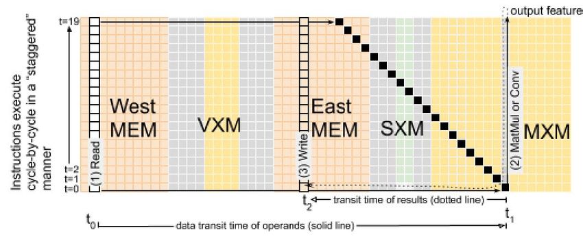
bank and a write of the results to the opposite bank of the             C. Optimizations
 SRAM. An example of this concurrency is shown in Figure 11,                The first revision of ResNet50 utilized algorithms that
 which shows the different operations (read, write, transpose,           distribute operations across the full chip to take advantage of
 rotate, etc) in a max pooling operation. From Figure 11 the             the compute performance of the MXM and VXM. A common
 solid lines show operand flow and dotted-line shows result               pattern in ResNet50 is Read → Conv2D → Requantize →
 data flow. We see the 16 concurrent streams are read from                ReLU → Write. The tensor sizes in ResNet50 layers are large
 memory by Read(1) and sent to the SXM where they undergo                enough to continuously stream data through the MXM and
 a transposition of their elements, and 16 stream results flow            VXM for up to several hundred cycles at a time. The next
 back to MEM where they are commited to SRAM by Write(1).                pipeline is not able to start until the functional slices be-
 From this figure, it is evident that each operation is preceded          came available for computation. The full tensor was streamed
 by read instructions to provide the stream operands and                 through the pipeline and written to memory as a delay before
 followed by a write to commit the results back to MEM.                  streaming the results through the next pipeline.
    Conventional CPUs rely on a memory hierarchy to implic-                 This approach to pipeline the different layers left resources
 itly move data between caches to service load/store operations.         under utilized at the beginning and end of the streaming
 Cache hierarchies introduce a reactive agent in the data path           operations as latency bubbles were created as the pipeline
 and the undesired unpredictability, or non-determinism, in the          filled and emptied. The initial memory allocations prevented
 data path to provide the illusion of sequentially consistent            starting the next pipeline when the previous pipeline was
 memory transactions within the memory hierarchy. The TSP’s              emptying due to memory slice contention. By adjusting the
 MEM system is unlike a conventional CPUs. Instead, we                   memory allocation patterns of input and output tensors to
 provide a thin layer of memory management that is used to               distribute the data across multiple slices. Interleaving banks
 identify the memory concurrency on an operation by operation            within the memory slice was carefully orchestrated so that we
 basis. As an example, the code below shows the memory                   were able to read a previous pipeline’s output from memory
 management for a transpose operation; an instruction that take          before the previous pipeline had completed writing its results.
 16 streams as input and creates 16 streams of output. The               These optimizations further reduced the overall latency of our
 malloc function returns a tensor of addresses allocated across          ResNet50 implementation by approximately 5,500 cycles to
 16 memory slices, one for each concurrent stream.                       our current performance of 20.4K IPS.
 1   # Read from 16 slices onto 16 streams                               D. Quantization
 2   # Transpose data
 3   # Write from 16 streams into 16 slices                                 For our initial implementation of ResNet50 we selected a
 4   import groq as g                                                    post-training layer-based symmetric int8 quantization strategy
 5   tensor = g.random_tensor(shape=[1024, 320],
 6       dtype=g.Int8, layout=[64, 16])                                  for convolutions and matrix multiplies. The MXM accepts int8
 7   streams_16 = tensor.read(streams=range(16))                         or fp16 inputs and accumulates to int32 or fp32 respectively.
 8   streams_16_t = g.transpose16(streams_16)                            These values are then requantized back to int8 or fp16. The
 9   out_addrs = g.malloc(shape=[1024, 320],
10                        layout=[64, 16])                               VXM has fp32 capacity to stream at the same rate of output
11   streams_16_t.write(out_addrs)                                       produced by the 4 MXM planes. This approach enabled higher
                    Listing 2. Memory management.
                                                                         precision across operations between matrix multiplies and
                                                                         convolutions improving the model’s overall precision. This
                                                                         resulted and a smaller quantization loss of 0.5% compared to
 B. Resource bottlenecks                                                 quantizing each operation. This initial approach leaves room to
                                                                         improve. The streaming architecture has capacity for an axis-
    To maximize value of on-chip resources we want to fully              based asymmetric quantization approach which will be used
 utilize the most expensive resources, which in the TSP’s                on future revisions and will reduce quantization accuracy loss.
 case is the MXM’s four (4) 320x320 MACC arrays and
 the MEM slices feeding them. In our implementation of                   E. Model Accuracy
 ResNet50 we found that the available ALU resources were                    The MXM has capacity for 320×320 matrix multiply. The
 well-balanced between the most computationally expensive                channel depths of the layers in ResNet50 are powers of 2.
 operations (convolution and matrix multiply) which were able            The input and output channel depths of convolutions determine
 to stream results at full bandwidth through the VXM to                  the dimensions of the weights. The misalignment between the
 perform requantization and ReLU operations in preparation               320×320 capacity and the 256×256 dimensions of weights
 for the next layer’s operations. There were limited situations          split across multiple passes under-utilizes the MXM. By fitting
 where the VXM ALU resources could not stream at the full                the model to the capacity of the MXM we are able to increase
 bandwidth due to number of operations that needed to be                 the number of computations without additional latency.
 performed by the VXMs (ie. depth of operations in a software               We trained an alternative version of ResNet50 with in-
 pipeline), the throughput delay was short, or minimized by the          creased channel depths to take advantage of MXM capac-
 parallelism across VXM ALUs and the concurrency available               ity. We found the additional weights contributed to higher
 within each ALU for Int8 data.                                          accuracy in the fp32 model. The standard ResNet50 trained

                                                                   154
to an accuracy of 75.6% Top-1 and 92.8% Top-5 while the
alternative version, taking full advantage of the 320-element
VL, trained to an accuracy of 77.2% Top-1 and 93.6% Top-5.
This encouraging result demonstrates how to exploit additional
model capacity when using the maxVL of 320 to improve
accuracy for the same computational cost and latency.
F. Deterministic performance
The TSP’s hardware eliminates arbiters and other reactive
elements in the data path, making performance deterministic
and precisely predictable from run-to-run execution. Within
the ResNet50 model we can determine the exact latency
of each layer. ResNet101 and ResNet152 match ResNet50’s
structure with the exception of a repeated set of additional
layers. From the demonstrated performance of ResNet50 on
the TSP we can project the performance of ResNet101 and
ResNet152 to the cycle. Based on our current ResNet50 Fig. 10. Power usage for ResNet50 layers.
implementation our ResNet101 throughput will be 14.3k IPS
a) Operating regimes: The roofline diagram [57] in
and ResNet152 throughput will be 10.7k IPS.
Figure 9 provides an intuitive framework for understanding
the different operating regimes of the chip, limited by either
V. D ISCUSSION (i) on-chip memory bandwidth, or (ii) arithmetic performance
This section describes initial proof-points and performance as delineated by the sloped peak in the diagram. The sloped
results of mapping the ResNet50 [27] v2 image classification region indicates where the TSP becomes memory bandwidth
model to our underlying tensor streaming processor. To preface bound loading weights into the MXM array for a subsequent
our discussion, the authors would like to point out that we conv2D or MatMul. The “roofline peak” indicates the satu-
received silicon back from the fab in July of 2019, just five (5) ration point where the arithmetic units are operating at peak
months before the ISCA paper deadline. In that brief timespan, utilization and we are subsequently arithmetically limited.
we validated A0 silicon and implemented ResNet50 on a new b) Matrix operations: Matrix operations are the
architecture, compiler, assembler, and tool chain for debugging workhorse of ML workloads, and the MEM slices can read
and visualization. Nevertheless, our initial implementation of 409,600 weights from memory and install them into the four
ResNet50 was a proof-point and reference model for compiler (4) 320×320 MXM arrays in less than 40 cycles including
validation, performing an inference query of the ResNet model SRAM and on-chip network transit delay! This is only
in < 43μs, yielding a throughput of 20.4K images per second possible because the MEM slices deliver 32 1-byte stream
with each image sample being a separate query (ie. batch size operands for each of the 320 parallel lanes, or 10 TiB/s of
of 1). That represents a 2.5× speedup relative to the Google operand stream bandwidth into the MXMs. The labeled data
TPU v3 [44] large batch inference. Perhaps more importantly, points are measured results with model weights laid out in
the TSP has an inference latency of only 49 μs for a single MEM so that we locate them toward the middle of the chip
image sample, which is nearly a 5× reduction in end-to-end in MEM slices — that is, ideally the compiler will layout
latency compared to Intel/Habana’s Goya [1] inference chip tensors in MEM slices so that data transit from memory slice
which takes 240 μs for batch 1 inference [44]. MEMi to MXM is minimized.
c) On-chip network: Typically, on-chip communication
has been carried out by routing packets [19] among cores,
whereby packets undergo routing, arbitration, and output port
scheduling, and as such often incur conflicts, thus introducing
nondeterminism and requiring flow control [16], [17]. How-
ever, on each tick of the core clock, the TSP propagates stream
values by one stream register hop in the direction of flow as
shown in Figure 4. The TSP hardware does not track the origin
or destination slice, instead streams simply flow (propagate)
Eastward or Westward until they fall off the edge of the chip or
are overwritten by a functional slice. In contrast to this more
conventional on-chip network, the TSP uses stream registers
(numbered in Figure 4) within each MEM to move data in the
Fig. 9. Roofline diagram showing arithmetic throughput (at 1 GHz core clock) X-dimension (superlane), and uses the SXM to move data in
varying with offered load. the Y-dimension on-chip through lane permutation.
155Fig. 11. Example instruction schedule for 3x3 max pool in ResNet50.
VI. R ELATED WORK VII. C ONCLUSION
GraphCore’s IPU [25] uses more than 1200 cores each with In this paper, we have introduced a novel hardware archi-
256 Kibytes of SRAM storage, approximately 300 Mibytes tecture of the first-generation Groq tensor streaming processor
of capacity for model parameters. However, GraphCore’s IPU (TSP). The TSP architecture reorganizes a conventional 2D
uses bulk-synchronous communication, which performs an mesh of cores into a functionally-sliced tiled microarchitecture
implicit synchronization. In contrast, our stream programming that scales from a minVL of 16-elements to a maxVL of
model does not require explicit synchronization of producer 320-elements. It is able to exploit dataflow locality within a
and consumers, except once at the beginning of the program. superlane to dramatically reduce latency. The abundant on-chip
Coarse-grain reconfigureable architectures (CGRAs) [47] memory bandwidth is able to concurrently feed the four (4)
focus on the highly regular communication patterns and image MXM arrays of 320×320 MACC (multiply-accumulate) cores
transforms that make ML workloads embarrassingly data for MatMul and conv2D operations, which are the workhorses
parallel. They map tensor operations to underlying hardware of many ML applications. Further, each of the 320 parallel
primitives of pattern memory unit (PMU) and pattern compute lanes have access to 16 powerful vector processors, for a total
unit (PCU). The Stanford Imagine [35] and Merrimac [18] of 5,120 vector ALUs on-chip, capable of 32-bit fixed and
stream supercomputer map stream constructs to the underly- floating point operations. Supporting both int8 and fp16 native
ing programming hierarchy of a local register file and each data types allows a single-chip solution for both quantized
compute cluster has access to its own bank of a stream register inference models and model training with floating point.
file for communication between clusters. In contrast, the TSP Modern ASIC technology yields ≈25 billion transistors on
architecture does not have any local register files, or FIFOs a single die. Broadly speaking, we are spending transistors on
for communicating, instead relying on a chip-wide set of (1) fixed or floating-point ALUs for arithmetic, and (2) storage
streaming registers for communicating results between the and communicating data among the available ALUs. We want
processing elements in each functional slice. to maximize the number of ALUs that we can stream operands
Prior research [5], [9], [23], [26], [32], [33], [38], [51] into at full bandwidth. In effect, our “conversion rate” for how
reduces off-chip communication by leveraging processing in well the architecture can extract value from the underlying
memory, variable bit width, compression, or locality-aware CMOS technology is measured by the number of deep learning
design. Since the TSP contains large amount of deterministic operations we can perform (ie raw performance) normalized
memory, we avoid frequently accessing off-chip memory. for transistor count. The first-generation Groq TSP (at 1 GHz)
Several prior proposals explore pruning based on sparsity [45], in 14nm ASIC and packaged as a PCIe CEM form factor,
[60], based on model- or domain-specific data patterns [4], yields a peak performance of 820 TeraOps/sec from 26.8B
[22], [24], [28]–[30], [36], [41], [50], [54], [61], [62], or transistors on-chip — 30K deep learning Ops/sec/transistor.
communication optimizations [39], [40], [53]. The TSP does Comparatively, Volta 100 which is capable of 130 TeraFlops
not use such optimizations to maintain a strictly deterministic of mixed-precision arithmetic, from 21.1B transistors in 815
execution time and power profile. mm2 implemented in a 12nm ASIC node — yielding 6.2K
156You can also read