Three-Wave Mixing Kinetic Inductance Traveling-Wave Amplifier with Near-Quantum-Limited Noise Performance
←
→
Page content transcription
If your browser does not render page correctly, please read the page content below
PRX QUANTUM 2, 010302 (2021)

                Three-Wave Mixing Kinetic Inductance Traveling-Wave Amplifier with
                           Near-Quantum-Limited Noise Performance
            M. Malnou ,1,2,* M.R. Vissers,1 J.D. Wheeler,1 J. Aumentado ,1 J. Hubmayr,1 J.N. Ullom,1,2 and
                                                       J. Gao1,2
                          1
                              National Institute of Standards and Technology, Boulder, Colorado 80305, USA
                          2
                              Department of Physics, University of Colorado, Boulder, Colorado 80309, USA

                (Received 30 June 2020; revised 2 November 2020; accepted 8 December 2020; published 5 January 2021)

                 We present a theoretical model and experimental characterization of a microwave kinetic inductance
              traveling-wave (KIT) amplifier, whose noise performance, measured by a shot-noise tunnel junction
              (SNTJ), approaches the quantum limit. Biased with a dc current, this amplifier operates in a three-wave
              mixing fashion, thereby reducing by several orders of magnitude the power of the microwave pump tone
              and associated parasitic heating compared to conventional four-wave mixing KIT amplifier devices. It
              consists of a 50  artificial transmission line whose dispersion allows for a controlled amplification band-
              width. We measure 16.5+1−1.3 dB of gain across a 2 GHz bandwidth with an input 1 dB compression power of
              −63 dBm, in qualitative agreement with theory. Using a theoretical framework that accounts for the SNTJ-
              generated noise entering both the signal and idler ports of the KIT amplifier, we measure the system-added
              noise of an amplification chain that integrates the KIT amplifier as the first amplifier. This system-added
              noise, 3.1 ± 0.6 quanta (equivalent to 0.66 ± 0.15 K) between 3.5 and 5.5 GHz, is the one that a device
              replacing the SNTJ in that chain would see. This KIT amplifier is therefore suitable to read large arrays of
              microwave kinetic inductance detectors and promising for multiplexed superconducting qubit readout.

              DOI: 10.1103/PRXQuantum.2.010302

                    I. INTRODUCTION                                  power handling capabilities as their resonant counterparts.
                                                                     Recent studies [16–18] suggest that a three-wave mix-
   Is it possible to build a quantum-limited microwave
                                                                     ing (3WM) JTWPA with a finely controlled and canceled
amplifier with enough gain, bandwidth and power han-
                                                                     Kerr nonlinearity should increase the device’s power han-
dling to simultaneously read thousands of frequency-
                                                                     dling tenfold. Compelling experiments have yet to prove
multiplexed superconducting resonators, like those in
                                                                     the feasibility of this approach, for which the JTWPA’s
qubit systems or microwave kinetic inductance detec-
                                                                     design and fabrication increase in complexity. We propose
tors (MKIDs)? When designed with resonant struc-
                                                                     to tackle this challenge using a different nonlinear medium:
tures, Josephson-junction-based parametric amplifiers
                                                                     starting with the intrinsic broadband and high power han-
have demonstrated high gain and quantum-limited per-
                                                                     dling capabilities of a kinetic inductance traveling-wave
formances [1–7]. However, despite efforts to increase the
                                                                     (KIT) amplifier [19], we build a near-quantum-limited
bandwidth up to a few hundred megahertz via impedance
                                                                     amplifier.
engineering [8,9], or to increase the power handling up to
                                                                        The current limitations on microwave amplification
a few hundred femtowatts via Kerr engineering [10–12],
                                                                     affect many scientific endeavors. Although proof-of-
they still cannot read more than a handful of resonators
                                                                     principle “quantum supremacy” was demonstrated by a
simultaneously. When designed with nonresonant struc-
                                                                     quantum computer containing a few tens of qubits [20],
tures, i.e., transmission lines, Josephson traveling-wave
                                                                     this number has to scale by at least an order of mag-
parametric amplifiers (JTWPAs) have high gain over giga-
                                                                     nitude to run powerful quantum algorithms [21,22]. In
hertz bandwidth [13–15], but so far still exhibit similar
                                                                     the hunt for exoplanets, cameras with tens of thousands
                                                                     of MKID pixels are being built [23], and proposals to
  *                                                                  search for very light warm dark matter also necessi-
      maxime.malnou@nist.gov
                                                                     tate the use of a great number of MKID pixels [24,
Published by the American Physical Society under the terms of
the Creative Commons Attribution 4.0 International license. Fur-     25]. All these applications are either already limited by
ther distribution of this work must maintain attribution to the      amplifier noise, or would greatly benefit from wideband,
author(s) and the published article’s title, journal citation, and   high gain, high power handling, quantum-limited ampli-
DOI.                                                                 fiers.

2691-3399/21/2(1)/010302(17)                                   010302-1              Published by the American Physical Society
M. MALNOU et al.                                                                         PRX QUANTUM 2, 010302 (2021)

   The KIT amplifier we present in this article is a                Solving the coupled mode equations (CMEs) for a pump
step toward a practical, quantum-limited amplifier, whose        at frequency ωp , signal at ωs , and idler at ωi , such that
bandwidth and power handling are compatible with high           ωp = ωs + ωi yields the 3WM phase-matching condition
channel-count applications. Operating in a 3WM fashion,         for exponential gain:
and fabricated out of a single layer of NbTiN, it consists
of a weakly dispersive artificial transmission line [26,27],                               ξ Ip0
                                                                                             2
for which we control the phase-matched bandwidth with                           k = −            (kp − 2ks − 2ki );            (2)
dispersion engineering. This limits spurious parametric                                     8
conversion processes that otherwise degrade the power
handling and noise performance. We measure an average           see Appendix A 1. Here, k = kp − ks − ki with kj , j ∈
gain of 16.5 dB over a 2 GHz bandwidth, and a typi-             {p, s, i}, the pump, signal, and idler wavenumbers, and Ip0
cal 1 dB input compression power of −63 dBm within              is the rf pump amplitude at the KIT amplifier’s input.
that bandwidth. Using a shot-noise tunnel junction (SNTJ)       In a nondispersive transmission line k = 0, and thus
[28,29] we measure the added noise of a readout chain with      Eq. (2) can naturally be fulfilled over a very wide fre-
the KIT amplifier as the first amplifier. To quote the true        quency range in KIT amplifiers, where Ip0  I∗ . Although
system-added noise of the chain, i.e., the one that a device    desirable within the amplification bandwidth, it is undesir-
replacing the SNTJ in that chain would see, we develop a        able outside of that bandwidth, where multiple paramet-
novel theoretical framework that accounts for the SNTJ-         ric conversion processes take place [30,31]. These pro-
generated noise illuminating both the signal and idler ports    cesses deplete the pump, thereby degrading the amplifier’s
of the KIT amplifier. Failure to account for the idler port’s    power handling, and they also induce multiple conver-
noise makes the system-added noise look significantly bet-       sion mechanisms at each frequency, thereby increasing the
ter than its true value. We demonstrate a true system-added     amplifier-added noise.
noise of 3.1 ± 0.6 quanta between 3.5 and 5.5 GHz, and             While in conventional traveling-wave amplifiers disper-
estimate that the KIT amplifier alone is near quantum lim-       sion engineering prevents only pump harmonic generation,
ited. It is the first time that the broadband noise properties   we suppress all unwanted parametric conversion processes
of a KIT amplifier are fully characterized rigorously.           by designing our amplifier as a weakly dispersive artificial
                                                                transmission line. Originally developed to have the KIT
              II. THEORY AND DESIGN                             amplifier matched to 50  [26], this line consists of a series
                                                                of coplanar waveguide (CPW) sections, or cells, each
   KIT amplifiers exploit the nonlinear kinetic inductance       with inductance Ld , flanked by two interdigitated capaci-
of a superconducting line to generate parametric interac-       tor (IDC) fingers √ that form the capacitance to ground C,
tion between pump, signal, and idler photons. In 3WM, a         such that Z = Ld /C = 50 ; see Fig. 1(a). Each IDC fin-
single pump photon converts into signal and idler photons,      ger then constitutes a low-Q, quarter-wave resonator, with
whereas four-wave mixing (4WM) converts two pump                capacitance Cf = C/2 and inductance Lf [see Fig. 1(b)],
                                                                                                             choose ωf =
photons in this fashion. Operating a KIT amplifier with          setby the finger’s length. In practice, we
3WM offers two key advantages over 4WM. First, as                1/ Lf Cf = 2π × 36 GHz, and Q = 1/Z Lf /Cf = 3.3,
the pump frequency is far detuned from the amplification         to generate a slight dispersion at low frequencies, where
band, it is easily filtered, which is often necessary to avoid   the pump, signal, and idler modes lie. The dashed line
saturating the following amplifier. Second, it reduces the rf
pump power because energy is extracted from dc power to
convert pump photons, which avoids undesirable heating            (a)                             (b)
effects from the strong rf pump, including those happening
in the packaging. More precisely, when biased with a dc
current Id , the KIT amplifier inductance per unit length L
is [30]

             L = Ld [1 + I + ξ I 2 + O(I 3 )],          (1)

where I is the rf current, Ld is the amplifier inductance
under dc bias, at zero rf current,  = 2Id /(I∗2 + Id2 ), and
                                                                FIG. 1. Schematic of the KIT amplifier artificial transmission
ξ = 1/(I∗2 + Id2 ). The current I∗ sets the scale of the non-   line. (a) Three cells in series (not to scale) are arranged in a CPW
linearity; it is typically approximately 103 higher than that   topology. The highly inductive central line (red) is flanked by
of Josephson devices, thereby conferring KIT amplifiers          IDC fingers, which match it to 50 . Each finger constitutes
approximately 104 –106 higher power handling capabili-          a low-Q, quarter-wave resonator. (b) In the equivalent electri-
ties than their Josephson equivalents. The term I permits      cal circuit, each cell consists of a series inductance Ld and two
3WM, while ξ I 2 permits 4WM.                                   resonators with inductance Lf and capacitance to ground C/2.

                                                          010302-2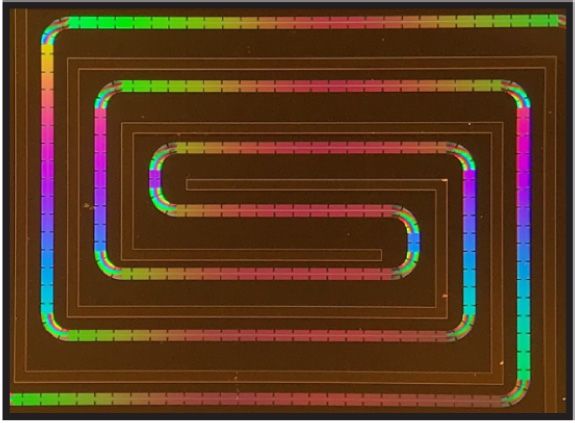
THREE-WAVE MIXING KINETIC INDUCTANCE...                                                           PRX QUANTUM 2, 010302 (2021)

                                                                          amplifier length, and with δL , the relative inductance mod-
                        (a)                                               ulation amplitude generated by the rf current and scaling
                               s         i                p
        k* (rad/cell)                                                     with Id . More precisely, the phase matched, small signal
                                                                          power gain can be written as
                                                                                                          1
                                                                                             Gs  cosh2      δ k N
                                                                                                            8 L p c
                                                                                                                          ,            (3)

                                                                          where Nc is the total number of cells; see Appendix A 2.
                                                                          Typically, when operating our KIT amplifier, δL ∼ 7 ×
                        (b)                                               10−3 ; thus, with Ld ∼ 50 pH/cell (see Sec. III), we need
                                                                          Nc > 5 × 10⁴ to get Gs > 15 dB at ωp ∼ 2π × 9 GHz.
                                                                             Since maximum gain is achieved with phase matching,
      G (dB)

                                                                          ωp influences the gain profile. To calculate this profile,
                                                                          we insert the dispersion relation k(ω) into the CMEs, and
                                                                          solve them numerically; see Appendix B. In Fig. 2(b) we
                                                                          show signal power gain profiles, calculated for the pump
                                                                          frequencies represented in Fig. 2(a). As expected, the gain
                                   f (GHz)                                is maximal at the signal and idler frequencies for which
                                                                          the triplets {ks , ki , kp } satisfy Eq. (2). When these frequen-
FIG. 2. Influence of the phase matching on the gain profile. (a)            cies are far apart, there is a region in between where phase
The nonlinear wavenumber k ∗ is calculated as a function of fre-          matching is not sufficient and the gain drops. By reduc-
quency for the transmission line represented in Fig. 1 (dashed),
                                                                          ing ωp , we can lower the distance between phase-matched
and for a similar line, periodically loaded at 80  (black). The
nonlinear part of four triplets {ks , ki , kp } that satisfy the phase-
                                                                          signal and idler frequencies, and therefore obtain a wide-
matching condition [Eq. (2)] are indicated with colored circles: in       band, flat gain region. Further reducing ωp , we reach the
purple ωi − ωs = 4 GHz, green ωi − ωs = 3 GHz, red ωi − ωs =              value where phase-matched signal and idler frequencies
2 GHz, and blue ωi = ωs . Additionally, a gray line indicates a           are equal, beyond what phase matching is nowhere fulfilled
pump frequency for which phase matching is nowhere fulfilled.              anymore, and the gain drops. Fundamentally, the wideband
(b) Solving the CMEs [Eqs. (A5)], the signal power gain pro-              nature of the gain depends on the convexity of the dis-
file is calculated [Eq. (A9)] for the related pump frequencies             persion relation, and therefore on the fingers’ length and
[the colors match with panel (a)]. The KIT amplifier length is             capacitance to ground. As ωf or Q increase, k ∗ is less
Nc = 6.6 × 10⁴ cells.                                                     convex, and thus closer to a broadband, phase-matched
                                                                          situation, but at the cost of allowing extra parametric
                                                                          processes to arise.

in Fig. 2(a) shows the dispersive
                               √      part of the wavenum-
                                                                                  III. EXPERIMENTAL REALIZATION
ber k ∗ = k − k0 with k0 = ω Ld C, as a function of fre-
quency. It is calculated by cascading the ABCD matrices                      Because the kinetic inductance nonlinearity is weak, in
of the KIT amplifier cells; see Appendix B. As it slightly                 practice a KIT amplifier comprises a transmission line tens
deviates from zero, no triplet {ks , ki , kp } can satisfy Eq.            of centimeters long. To maximize this nonlinearity, and to
(2).To retrieve phase matching over a desired bandwidth,                  minimize its length, the line as well as IDC fingers are
we engineer another dispersion feature by increasing the                  made 1 μm wide, and each unit cell is 5 μm long; see
line impedance periodically on short sections. This feature               Figs. 3(a) and 3(b). Fabricated from a 20 nm thick NbTiN
creates a resonance in the line’s phase response (and a stop-             layer on 380 μm high-resistivity intrinsic silicon via opti-
band in the line’s amplitude response), at a frequency ωl                 cal lithography, it yields I∗ ∼ 7 mA, and a sheet inductance
controlled by the loading periodicity [26,32]. In Fig. 2(a)               of approximately 10 pH/square. Thus, Ld ∼ 50 pH, and
we show k ∗ in a line periodically loaded at 80 , with                   in order to retrieve Z = 50 , each finger is made 102
ωl = 2π × 8.5 GHz. Because the nonlinear wavenumber                       μm long. The loading [Fig. 3(a)] consists of cells with
close to resonance varies sharply, there exists values of kp∗             shorter fingers (33.5 μm, Z = 80 ), arranged periodically
(above ωl ) for which we can find triplets {ks , ki , kp } that sat-       to generate a resonance at 8.5 GHz, thereby positioning
isfy Eq. (2) (examples of their nonlinear parts are shown                 the pump frequency in a way compatible with our filtering
with colored circles). A slight variation of the pump fre-                capabilities.
quency ωp significantly affects which pair of signal and                       We lay out the line in a spiral topology, on a 2 ×
idler frequencies is phase matched.                                       2 cm chip [Fig. 3(c)], which contains Nc = 6.6 × 10⁴
   At these matched frequencies, the 3WM gain grows                       cells, equivalent to 33 cm. To avoid spurious chip and
exponentially with kp (in radians per cell), with the KIT                 microstrip modes, electrical grounding inside the chip is

                                                                   010302-3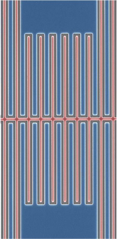
M. MALNOU et al. PRX QUANTUM 2, 010302 (2021)
(a) (b)
G (dB)
(a)
(b)
G (dB)
Pt (dBm)
1 µm
G (dB)
(c) (c)
f (GHz) f (GHz)
FIG. 4. Amplification properties of the KIT amplifier. (a) The
10 µm power gain is measured with a vector network analyzer (VNA),
when ωp = 2π × 8.895 GHz (blue), and ωp = 2π × 8.931 GHz
FIG. 3. Micrographs of the KIT amplifier. (a) The transmis- (red). (b) The gain of a probe tone at 4.5 GHz compresses as
sion line (false color red) is periodically loaded with shorter IDC the tone’s power increases. At P−1 dB = −63 dBm, referred to
fingers. (b) Line and fingers are 1 μm wide, and each cell is the KIT amplifier’s input, the gain has lowered by 1 dB from
5 μm long. (c) The overall KIT amplifier is laid out in a spi- its small signal value. It is measured for ωp = 2π × 8.895 GHz.
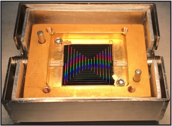
ral configuration on a 2 × 2 cm chip, and clamped on a copper (c) At the same pump frequency, a closeup on the small signal
packaging. gain around 4.5 GHz shows ripples with 8 MHz characteristic
frequency.
ensured with spring-loaded pogo pins, descending from the
top copper lid of the packaging, and contacting the chip tone. The gain compresses by 1 dB from its small signal
between the line traces; see Appendix D. The pogo pins value for P−1 dB = −63 dBm, about 7 dB lower than the-
also improve the chip-to-packaging thermal link, which oretical predictions; see Appendix C 2. This discrepancy,
otherwise mostly relies on wire bonds. suggesting substantial room for improvement, may be due
In a first experiment, we measure the gain, bandwidth, to effects not included in our model, such as standing-
and power handling of the KIT amplifier when cooled to wave patterns, or defects in the line, which locally lower
approximately 30 mK. It is mounted as the sole ampli- I∗ . Nonetheless, P−1 dB is already about 30 dB higher than
fier in the chain, thereby facilitating comparison of its JTWPAs [13–15], and about 10 dB less than 4WM KIT
gain profile to the theoretical profiles, and revealing the amplifiers with similar gain (see Appendix H). This ampli-
gain ripples of the isolated amplifier, which otherwise also fier is therefore suitable to read thousands of frequency
depend on the return loss of external components. Two multiplexed MKIDs that use drive tone powers typically
mandatory bias tees at the KIT amplifier input and out- around −90 dBm [27,30] or even more qubits, whose
put ports combine dc and rf currents. In Fig. 4(a) we show readout involves powers substantially less than −90 dBm.
KIT amplifier gain profiles, acquired at two different pump As in any phase-insensitive traveling-wave and res-
frequencies. The current amplitudes are Id = 1.5 mA and onant parametric amplifier, the practical, usable band-
Ip0 = 160 μA (−29 dBm in power, calibrated in situ by width is half of the presented amplification bandwidth.
comparing dc and rf nonlinear phase shifts; see Appendix It is the bandwidth in which signals coming from
A 3). For the higher pump frequency, the gain drops in the microwave devices can be phase-insensitively amplified.
middle of the amplification bandwidth. For the lower one, The other half, barring the idler frequencies, contains a
the gain profile is flatter, with an average value of 16.5+1
−1.3 copy of signals in the first half. That is why the gain in
dB between 3.5 and 5.5 GHz, where the subscript and Fig. 4(a) is nearly symmetric about the half pump fre-
superscript denote the amplitude of the gain ripples. Both quency (approximately 4.5 GHz). The asymmetry—gain
profiles agree qualitatively with behaviors explained in and ripples marginally bigger above the half pump fre-
Sec. II. The gain ripples have an 8 MHz characteristic fre- quency—originates from a frequency-dependent satura-
quency [see Fig. 4(c)], equivalent to√62.5 cm in wavelength tion power. In fact, higher frequencies possess a higher
(the phase velocity being vp = 1/ Ld C ∼ 1000 cells per saturation power; see Appendix C 1. We see this effect here
nanosecond), or about twice the KIT amplifier length. We because we chose a signal power close to P−1 dB in order
thus attribute their presence to a mismatch in impedance to maximize the signal-to-noise ratio in this measurement,
between the KIT amplifier and the microwave feed struc- where the KIT amplifier remains the sole amplifier.
tures placed before and after it. This mismatch results in At higher dc current bias (bounded by the dc criti-
a pump standing-wave pattern, which influences the sig- cal current of the transmission line, approximately 2.4
nal amplification, depending on its frequency. In Fig. 4(b) mA in our device), lower rf pump power can be used
we show the gain at 4.5 GHz (obtained at the lower pump to obtain equivalent small signal gain, at the cost of a
power), as a function of Pt , the input power of a probe reduced 1 dB compression power. Conversely, reducing Id
010302-4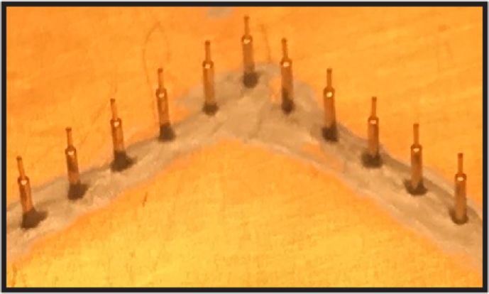
THREE-WAVE MIXING KINETIC INDUCTANCE...                                                       PRX QUANTUM 2, 010302 (2021)

and increasing Ip0 improves power handling capabilities,                                    Bias Pump
but the gain is then limited by a superconductivity break-
ing phenomenon. We suspect the presence of weak links
[33], and we are currently investigating the line breakdown
mechanism.
                                                                                                                                    SA

              IV. NOISE PERFORMANCE
   The combined gain, bandwidth, and power handling per-                   SNTJ

formance are promising, provided that the KIT amplifier                                                  30 mK              4K

also presents competitive noise performance. Measuring
this noise is a topic of current interest [19,27,34], and           FIG. 5. Schematic of the noise measurement setup. Each com-
we execute the task using a self-calibrated SNTJ [28,29].           ponent is labeled with its gain or transmission efficiency, and
We measure the output spectral density, whose power                 with its input-referred added noise. Calibrated noise Nins (Nini ) is
depends on the chain’s gain and loss. The SNTJ acts as              generated by the SNTJ at the signal (idler) frequency. It is routed
a dynamic variable noise source, allowing for a continuous          to the KIT amplifier with transmission efficiency η1s (η1i ), i.e.,
                                                                    it undergoes a beamsplitter interaction and part of it is replaced
sweep in input noise temperature by sweeping its bias volt-
                                                                    with vacuum noise whose value Nf = 0.5 quanta. At the KIT
age, and our measurement scans the entire KIT amplifier                                                  j
                                                                    amplifier’s input, the noise is N1 , j ∈ {s, i}. On the signal-to-
bandwidth.                                                                                                         s
                                                                    signal path, the KIT amplifier then adds Nex       quanta of excess
   Because the SNTJ is a wideband noise source, it illu-            noise and has a gain G; on the idler-to-signal path, the KIT ampli-
minates the KIT amplifier at both its signal and idler               fier adds Nex i
                                                                                   quanta of excess noise and has a gain G − 1. Noise
frequency inputs; these input noises are then parametri-            N2 at the KIT amplifier’s output is then routed with efficiency η2
                                                                       s

cally amplified. We thus model the KIT amplifier as a                 to the HEMT (input noise N3s ). With gain GH and added noise
three-port network: two inputs at ωs and ωi , and one out-          NH , it further directs the noise N4s to room-temperature compo-
put at ωs . In Fig. 5 we present a schematic of the entire          nents. Amplification and loss at room temperature are excluded
amplification chain, where we have labeled the gain or               from our schematic but not our analysis. The noise reaching the
transmission efficiency, and input-referred added noise of            spectrum analyzer (SA) is Nos . The full setup is described in
                                                                    Appendix E.
each component. The KIT amplifier power gain on the
signal-to-signal path is G, while its power gain on the idler-
to-signal path is G − 1 [35]. The output noise at the signal           In practice, we measure Nos while varying simultane-
frequency (in units of photons) measured on the SA can              ously Nins and Nini using the SNTJ voltage bias [Fig. 6(b)].
                                                                                                       s           i
then be written as                                                  We then fit to obtain Gss      si
                                                                                             c , Gc , Neff , and Neff (see Appendix
                                                                    F 3), and form N with Eq. (5). In Fig. 6(c) we present the
          Nos = Gss
                 c (Nin + Neff ) + Gc (Nin + Neff ),
                      s    s       si   i    i
                                                             (4)    system-added noise N , measured over the KIT amplifier’s
                                                                    amplification bandwidth. In this experimental configura-
where Nins (Nini ) is the SNTJ-generated noise at the signal        tion, the KIT amplifier gain is G = 16.6+1.8    −3.1 dB between
(idler) frequency, Gss     si
                       c (Gc ) is the signal-to-signal (idler-to-   3.5 and 5.5 GHz [Fig. 6(a)], stable over the acquisi-
signal) gain of the entire chain from the SNTJ to SA, and           tion time (approximately 12 h). In that bandwidth, N =
  s     i
Neff  (Neff ) is the effective signal-to-signal (idler-to-signal)      3.1 ± 0.6 quanta. It is an unprecedented broadband, true
path KIT amplifier excess noise; see Appendix F 1. When              system-added noise performance (see Appendix H).
varying Nins and Nini , we retrieve Neffs
                                         and Neffi
                                                  , equal to zero      This performance depends on the intrinsic signal (idler)
for a quantum-limited amplifier.                                     KIT amplifier excess noise Nex      s      i
                                                                                                           (Nex ), but also on the
   The system-added noise that a device replacing the               chain’s transmission efficiencies as well as on the HEMT-
SNTJ would see is therefore                                         added noise NH . More precisely, when {G, NH }  1, Eq.
                                                                    (5) becomes
                               Gsic
                N = Neff
                     s
                        +           (Nf + Neff
                                           i
                                              ),             (5)
                               Gss
                                c                                               s
                                                                               Nex + Nex
                                                                                      i
                                                                                           2(1 − η1s )Nf    NH
                                                                         N =             +               +         + Nf .            (6)
where Nf = 0.5 quanta is the vacuum noise (provided that                           η1
                                                                                    s
                                                                                                η1
                                                                                                 s
                                                                                                           η2 Gη1s
the idler port of this device is cold); for a high gain, phase-
insensitive quantum-limited amplifier Nf is the minimum              From left to right, the first three terms on the right-hand
added noise [35]. Failure to account for the additional             side represent the contribution to N from the KIT ampli-
change in idler noise at the amplifier’s input leads to an           fier alone, from the lossy link between the SNTJ and the
underestimate of the system-added noise by about a factor           KIT amplifier, and from the HEMT-added noise; the last
of two, thereby making it look significantly better than its         term is the minimum half quantum of added noise that
true value, given by Eq. (5); see Appendix F 2.                     a quantum-limited amplifier must add [35]. Measuring

                                                              010302-5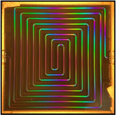
M. MALNOU et al.                                                                              PRX QUANTUM 2, 010302 (2021)

    G (dB)

               (a)

               (c)                                                                      QL             (b)
             3.0     3.5        4.0         4.5          5.0       5.5         6.0         6.5
                                                  f (GHz)

FIG. 6. System-added noise measurement of a microwave amplification chain with a KIT amplifier as the first amplifier. (a) The
gain’s frequency dependence is measured with a VNA (with a 1 kHz intermediate frequency bandwidth). (b) The output noise Nos is
measured with a SA (5 MHz resolution bandwidth, comparable to a typical resonant amplifier’s bandwidth), while varying the SNTJ
dc voltage bias V. Fitting the whole output noise response, we obtain the frequency-dependent system-added noise N and the chain’s
                        c . We divide No by Gc to refer it to the KIT amplifier input, and subtract the zero bias noise value Nf = 0.5,
signal-to-signal gain Gss               s     ss

so that N [panel (c)] visually matches the zero bias value of Nos (see Appendix F 3). Three colored curves indicate output noises at 4,
5, and 6 GHz, with fits superimposed in black lines. (c) Data from the output noise spectra are compiled to form N . Uncertainties are
indicated by the gray area surrounding the black line. They predominantly come from the fit of the curves in (b). The quantum limit
(QL) on amplifier-added noise is indicated by the dashed black line.

the individual loss of the chain’s components, we esti-              fabrication process, like electron beam lithography, may
mate the value of the transmission efficiencies to be η1s =            improve the performance of the device. Also, running the
0.57 ± 0.02 and η2 = 0.64 ± 0.10; in addition, by mea-               amplifier at higher gain will require better damping of the
suring the system-added noise of the amplification chain              gain ripples, whose amplitude grows with gain. Finally,
with the KIT amplifier turned off, we estimate NH = 8 ± 1              we are investigating the origin of the remaining excess
quanta; see Appendix G. With this additional information,            noise Nexs
                                                                                + Nex
                                                                                    i
                                                                                      . It may be due to parasitic chip heating
we estimate that the overall KIT amplifier excess noise is            or two-level system noise [36].
Nexs
     + Nex
         i
            = 0.77 ± 0.40 quanta, suggesting that the KIT
amplifier alone operates near the quantum limit.
    Several strategies can improve the system-added noise.
First, increasing the transmission efficiencies would have                                   V. CONCLUSION
a major impact, because all the system-dependent noise                  It is possible to build a microwave amplifier with
contributions are enlarged by 1/η1s . For example, η1s = 0.8         broadband and near-quantum-limited performance with-
would yield N = 1.6 quanta. To that end, we are cur-                 out sacrificing power handling capability. Engineering the
rently developing lossless superconducting circuits (bias            phase-matched bandwidth is key because it suppresses
tees, directional couplers, and low-pass filters) that can be         spurious parametric conversion processes. We demonstrate
integrated on chip with the KIT amplifier. Second, increas-           this idea on a KIT amplifier, whose combined gain, band-
ing the KIT amplifier gain G would reduce the HEMT                    width, power handling, and noise performance are fully
contribution to N [third term in Eq. (6)]. Here, this con-           characterized. In addition, we develop a theoretical frame-
tribution is estimated at 0.5 ± 0.3 quanta. The solutions to         work adapted to noise measurements performed with wide-
achieve higher gain directly follow from Eq. (3): higher             band noise sources. Using a SNTJ, we evaluate the true
pump power (i.e., increase δL ), longer line (increase Nc ), or      system-added noise of an amplification containing the KIT
higher inductance per unit cell (increase kp ). All represent        amplifier as the first amplifier. The KIT amplifier itself is
nontrivial challenges, starting with better understanding            estimated to be near quantum limited; therefore, it has the
the line breakdown mechanism [33]. If it comes from                  potential to initiate a qualitative shift in the way arrays
imperfections in the line (weak links), a higher resolution          of superconducting detectors, such as MKIDs, process

                                                               010302-6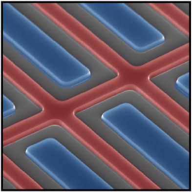
THREE-WAVE MIXING KINETIC INDUCTANCE...                                                            PRX QUANTUM 2, 010302 (2021)

information, moving them into a quantum-limited readout               case, because the phase-matching bandwidth is limited by
regime.                                                               dispersion engineering (see Appendix B), and thus mostly
                                                                      these three frequencies are able to mix together. Under
                 ACKNOWLEDGMENTS                                      the slow-varying envelope approximation, |d2 Ij /dx2 |
                                                                      |kj dIj /dx| for j ∈ {p, s, i}, the left-hand side of Eq. (A2)
   We thank Kim Hagen for his help in the design and
                                                                      yields
fabrication of the KIT amplifier packaging, and Felix Viet-
meyer and Terry Brown for their help in the design and
fabrication of room-temperature electronics. We acknowl-                         ∂ 2I  ∂ 2I                 dIj i(kj x−ωj t)
edge useful discussions with John Teufel, Gangqiang Liu,                   vp2        − 2 = vp2          ikj    e             + c.c.    (A4)
                                                                                 ∂x 2  ∂t       j =p,s,i
                                                                                                             dx
and Vidul Joshi. Certain commercial materials and equip-
ment are identified in this paper to foster understanding.
Such identification does not imply recommendation or                   Using ωp = ωs + ωi , we collect terms at ωj , j ∈ {p, s, i},
endorsement by the National Institute of Standards and                on the right-hand side (rhs) and form the CMEs
Technology, nor does it imply that the materials or equip-
ment identified are necessarily the best available for the
purpose. This work is supported by the NIST Innova-                     dIp   ikp                  ikp ξ
                                                                            =       Is Ii e−ik x +       Ip (|Ip |2 + 2|Is |2 + 2|Ii |2 ),
tions in Measurement Science Program, NASA under                        dx      4                     8
Grant No. NNH18ZDA001N-APRA, and the DOE Accel-                                                                                     (A5a)
erator and Detector Research Program under Grant No.                    dIs   iks  ∗ ik x iks ξ
89243020SSC000058.                                                          =      Ip Ii e +      Is (2|Ip |2 + |Is |2 + 2|Ii |2 ),
                                                                        dx      4             8
                                                                                                                               (A5b)
 APPENDIX A: COUPLED-MODE THEORY OF A
                                                                           dIi   iki  ∗ ik x iki ξ
        dc-BIASED KIT AMPLIFIER                                                =      Ip Is e +      Ii (2|Ip |2 + 2|Is |2 + |Ii |2 ),
                                                                           dx     4              8
                1. Coupled mode equations                                                                                          (A5c)
   The phase-matching condition for exponential gain, Eq.
(2), is obtained by solving the CMEs while pumping in
                                                                      with k = kp − ks − ki . The phase-matching condition,
a 3WM fashion, i.e., such that ωp = ωs + ωi , and in the
                                                                      Eq. (2), is found for a strong pump, where {|Is |, |Ii |}  |Ip |.
presence of 3WM and 4WM terms; see Eq. (1). The CMEs
                                                                      Assuming that the pump is undepleted, |Ip (x)| = Ip0 , Eqs.
relate the current amplitudes Ij , j ∈ {p, s, i}, at the frequen-
                                                                      (A5) can be rewritten as
cies ωj , j ∈ {p, s, i}; they are obtained by injecting Eq.
(1) into the telegrapher’s equations, and by operating the
harmonic balance (HB) with only these three frequencies.                                 dIp   ikp ξ 2
   More precisely, the telegrapher’s equations in a lossless                                 =       Ip Ip0 ,                          (A6a)
                                                                                         dx      8
transmission line relate current I and voltage V as                                      dIs   iks  ∗ ik x iks ξ 2
                                                                                             =      Ip Ii e   +   Is Ip0 ,             (A6b)
                ∂I   ∂V                  ∂V   ∂I                                         dx      4              4
              −    =C ,                −    =L ,               (A1)                      dIi   iki  ∗ ik x iki ξ 2
                ∂x   ∂t                  ∂x   ∂t                                             =      Ip Is e   +   Ii Ip0 ,             (A6c)
                                                                                          dx    4               4
with x a length per unit cell. Injecting Eq. (1) into Eq. (A1),
we obtain
                                                                    which results in Ip (x) = Ip0 exp (iξ kp Ip0   2
                                                                                                                       x/8). Signal and
              ∂ 2I   ∂ 2I       ∂ 1 2 1 3                             idler amplitudes are then searched with the form Ij (x) =
           vp2 2 − 2 = 2              I + ξ I             (A2)
              ∂x     ∂t        ∂t 2          3                        Ĩj (x) exp (iξ Ip0
                                                                                       2
                                                                                          kj x/4), j ∈ {s, i}. Equations (A6) then yield
              √
with vp = 1/ CLd the phase velocity. To solve Eq. (A2),
we perform the HB. We assume that the current in the                                           dĨs   iks
transmission line is a sum of three terms at three different                                         =       Ip0 Ĩi∗ eiβ x ,
                                                                                               dx       4
frequencies,                                                                                                                            (A7)
                                                                                               dĨi   iki
                                                                                                    =       Ip0 Ĩs∗ eiβ x ,
           I = 12 [Ip (x)ei(kp x−ωp t) + Is (x)ei(ks x−ωs t)                                   dx      4
                   + Ii (x)ei(ki x−ωi t) + c.c.],              (A3)
                                                                      with β = k + (ξ Ip0 2
                                                                                              /8)(kp − 2ks − 2ki ) and k = kp −
and we then keep only the mixing terms from Eq. (A2) that             ks − ki . The system of equations (A7) has known solutions
emerge at these frequencies. This approach is valid in our            [37]. In particular, when phase matching is achieved, i.e.,

                                                                010302-7
M. MALNOU et al. PRX QUANTUM 2, 010302 (2021)
β = 0, we obtain we can use the continued presence of 4WM to our advan-
tage, because it allows us to calibrate the pump power,
Ĩs = cosh (g3 x)Ĩs0 , down to the KIT amplifier input.
In fact, in such a situation Id and Ip0 influence the pump
ki (A8) tone phase shift, which we can measure unambiguously
Ĩi = i sinh (g3 x)Ĩs0 ,
ks (i.e., not mod 2π ) with a VNA. More precisely, although
the phase φ = arg(S21 ) read by a VNA is 2π wrapped, its
√ shift δφ = φ − φ0 from an initial value φ0 can be continu-
with g3 = (Ip0 /4) ki ks , and with initial conditions
Is (0) = Is0 and Ii (0) = 0. The signal power gain ously monitored when Id and Ip0 vary, and thus unambigu-
ously determined. This phase shift in turn translates into a
Is (x) 2 wavenumber variation δp = −δφ /Nc . If initially at zero dc
Gs (x) = (A9) bias and small rf pump amplitude, then δp = βp − kp , with
Is0
βp the pump wavenumber, dependent on Id and Ip0 , and kp
the linear wavenumber. When a single pump tone travels
is then exponential with x: Gs = cosh2 (g3 x).
along the line (no input signal), we are by default under the
strong pump approximation, and Eq. (A6a) gives Ip (x) =
2. 3WM gain Ip0 exp (iξ kp Ip0
2
x/8). In addition, the current I in the line
We can rewrite g3 as a function of more meaningful then writes as I = 12 {Ip (x) exp[i(kp x − ωp t)] + c.c.}, and
quantities. In fact, the linear inductance L exposed in Eq. thus the pump wavenumber is βp = ξ kp Ip0 2
/8 + kp , which
(1) also writes √
leads to δp = ξ kp Ip0 /8. Because kp = ωp Ld C, we can
2
rewrite
Id2 2Id I I2
L = L0 1 + 2 1+ 2 +
I∗ I∗ + Id2 I∗2 + Id2
1 Ip0
2
I2
2Id I δp = ωp L0 C 1 + d2 ; (A13)
Ld 1 + 2 , (A10) 8 I∗2 I∗
I∗ + Id2
therefore, Ip0 and Id induce similar phase shifts in the line.
when I Id , and with Ld = L0 (1 + Id2 /I∗2 ). Here, L0 is Knowing Id (room-temperature parameter), we thus get Ip0
the bare linear inductance. It is the one directly derived at the KIT amplifier input.
from the sheet kinetic inductance and the geometry of the
line, while Ld is the inductance per unit length under dc
APPENDIX B: ABCD TRANSFER MATRICES
bias. Because Id2 I∗2 , for design purposes, Ld ∼ L0 . In the
strong pump regime I = Ip0 ; therefore, 2Id I /(I∗2 + Id2 ) = The dispersion relations, Fig. 2(a), are calculated by
Ip0 ; assuming that ks = ki kp /2, we therefore obtain cascading the ABCD matrices of the KIT amplifier cells,
1 a method suitable for any periodic loading pattern. We
Gs (x) cosh2 δ k x
8 L p
, (A11) then compute the KIT amplifier S21 scattering parameter
as S21 = 2/(A + B/Z0 + CZ0 + D) [32], where Z0 = 50
where is the input and output ports impedance, and finally get
k = −unwrap[arg(S21 )]/Nc .
L − Ld 2Id Ip0 In the unloaded case, represented in Fig. 1, the ABCD
δL = = 2 (A12)
Ld I∗ + Id2 matrix cell is
⎡ ⎤
is the relative inductance variation due to Ip0 . With I∗ = 1 iLd ω
7 mA, and typical values Id = 1.5 mA (limited by the dc Tc = ⎣ i2Cω 2Ld Cω2 ⎦ . (B1)
critical current, approximately 2.4 mA, value specific to 1 −
2 − Lf Cω 2 2 − Lf Cω 2
our NbTiN film and to the line’s width) and Ip0 = I∗ /60,
we obtain δL = 6.8 × 10⁻³ . All the cells being identical, the KIT amplifier’s ABCD
matrix is simply TK = TNc c . In Fig. 2(a) we used Nc =
3. Pump phase shift 6.6 × 10⁴ to match the length of our fabricated KIT ampli-
From the phase-matching condition, Eq. (2), it is clear fier, and Ld = 45.2 pH, C = 18.8 fF, and Lf = 1.02 nH,
that only the 4WM term ξ creates a dispersive phase shift values that match our design (fingers are 102 μm long and
of pump, signal, and idler. In other words, in a pure 3WM 1 μm wide).
case, ξ = 0 and the phase-matching condition becomes In the loaded case, some cells have shorter fingers;
k = 0, naturally fulfilled in a dispersionless transmission see Fig. 3(a). In these cells, the capacitance to ground is
line. While detrimental for noise properties (see Sec. IV), Cl = Ld /Zl2 , where Zl is the load impedance, and a finger’s
010302-8THREE-WAVE MIXING KINETIC INDUCTANCE... PRX QUANTUM 2, 010302 (2021)
inductance is Ll . To compute the KIT amplifier scatter-
ing parameter, we form the ABCD matrix of the repetition (a)
pattern comprised with unloaded and loaded cells:
G (dB)
⎡ ⎤Nu /2
1 iLd ω
Tsc = ⎣ i2Cω 2Ld Cω2 ⎦
1 −
2 − Lf Cω2 2 − Lf Cω2
⎡ ⎤Nl
1 iLd ω f (GHz)
× ⎣ i2Cl ω 2Ld Cl ω2 ⎦
1 − (b) (c)
2 − Ll Cl ω2 2 − Ll Cl ω2
P–1 dB (dBm)
⎡ ⎤Nu /2
G (dB)
1 iLd ω
× ⎣ i2Cω 2Ld Cω2 ⎦ . (B2)
1 −
2 − Lf Cω2 2 − Lf Cω2
Here Nu is the number of unloaded cells and Nl is the num-
Pt (dBm) f (GHz)
ber of loaded cells in the pattern, which we call a supercell.
As before, to get the KIT amplifier’s ABCD matrix, we
simply form TK = TNscsc , where Nsc = Nc /(Nu + Nl ) is the FIG. 7. Theory of KIT amplifier saturation, calculated by solv-
number of supercells in the KIT amplifier. Here, Nu = 60 ing the full CMEs, Eqs. (A5). (a) Distortion of the gain profile,
at four different input signals: Is0 = Ip0 /100 (blue curve), cor-
(equivalent to 300 μm), Nl = 6 (equivalent to 30 μm),
responding to a small signal regime, Is0 = Ip0 /12 (red curve),
Nc = 66 000 (equivalent to 33 cm); therefore, Nsc = 1000. Is0 = Ip0 /8 (green curve), and Is0 = Ip0 /6 (purple curve). The
The solid line in Fig. 2(a) shows the wavenumber k ∗ thus KIT amplifier length is Nc = 6.6 × 10⁴ cells. Vertical lines indi-
found, with Zl = 80 , and Ll = 335 pH, as the finger cate three frequencies: 3.4406 GHz (long dashed), 4.4406 GHz
length in a loaded cell is 33.5 μm. (solid), equal to the half pump frequency, and 5.4406 GHz (short
To compute the signal power gain, Fig. 2(b), we inject dashed). (b) The gain of a probe tone is calculated at these three
the expression of k(ω) for a periodically loaded KIT ampli- frequencies, as a function of the probe tone power. (c) The 1 dB
fier (from TK ) in the CMEs, Eqs. (A5). We solve them compression power is shown as a function of frequency.
numerically for different pump frequencies. For 8.8812
GHz (blue curve), 8.8992 GHz (red curve), 8.9256 GHz Fundamentally, this asymmetry stems from the fact that,
(green curve), and 8.9736 GHz (purple curve), the phase- when solving the CMEs in the case where Ip varies along
matched signal and idler are detuned from the half pump the KIT amplifier transmission line, the initial conditions
frequency by 0, 1, 1.5, and 2 GHz, respectively. For 8.855 (ICs) vary as a function of frequency. More precisely,
GHz (gray curve), phase matching is nowhere achieved. Eqs. (A5b) and (A5c) govern the evolution of Is and Ii ,
We used Nc = 6.6 × 10⁴ , I∗ = 7 mA, Id = 1.5 mA, and the respectively; in a simplified version, they read
initial conditions Ip0 = I∗ /60, Is0 = Ip0 /100, and Ii0 = 0,
close to experimental values. dIs iks ∗
= Ip Ii ,
dx 4
(C1)
APPENDIX C: KIT AMPLIFIER SATURATION dIi iki ∗
= Ip Is .
1. Strong signal gain profile asymmetry dx 4
When the input signal power amounts to a signifi-
We dropped the second terms on the rhs of Eqs. (A5b) and
cant fraction of the pump power, parametric amplification
(A5c), representing the 4WM conversion processes, as the
depletes the pump. It surprisingly generates asymmetry
asymmetry still holds when ξ = 0, and we assumed per-
in the signal gain profile, with respect to the half pump
fect phase matching in 3WM, k = 0, i.e., a dispersionless
frequency. In Fig. 7(a) we show signal gain profiles, cal-
line.
culated when phase matching is achieved at exactly half
In the undepleted pump regime Ip (x) = Ip0 , and we can
the pump frequency, i.e., for ωs = ωi (corresponding to
decouple the equations on Is and Ii . Differentiating Eqs.
ωp = 8.8812 GHz), at various initial signal powers Ps0 .
(C1) with respect to x, we get
They are obtained by solving the CMEs, Eqs. (A5), which
incorporate pump depletion effects. As Ps0 increases, the
gain diminishes, and the originally flat profile tilts, with d2 Ij
= g32 Ij (C2)
higher frequencies presenting higher gain. dx2
010302-9M. MALNOU et al. PRX QUANTUM 2, 010302 (2021)
√
with j ∈ {s, i} and g3 = (Ip0 /4) ki ks , as defined in (a) (c)
Appendix A 1. Using the ICs Is (0) = Is0 and dIs /dx(0) = 0
[because Ii∗ (0) = 0], Is = cosh(g3 x)Is0 , as seen in Eqs.
(A8). Signal and idler wavenumbers appear as a product
in this solution; hence, for any x, the signal amplitude Is is
symmetric with respect to the half pump frequency.
In the soft pump regime, where Ip (x) is not constant,
Eqs. (C1) cannot be decoupled. We can however write (b) (d)
them in a canonical form, differentiating with respect to
x:
d2 Ij 1 dIp dIj ks ki 2
− − |Ip |2 Ij = 0 (C3) 2.85 mm
dx2 Ip dx dx 16
with j ∈ {s, i}. Here, the interplay between Is and Ii FIG. 8. KIT amplifier packaging. (a) The amplifier is clamped
comes from Ip , which contains the product Is Ii [see Eqs. on a gold plated copper box and wire bonded to PCBs and to
(A5)]. Although signal and idler wavenumbers also appear the box itself. Although not very sensitive to the magnetic field,
only as a product in Eq. (C3), these CMEs lead to an the KIT amplifier is shielded with aluminum and A4K cryogenic
shielding. Two SMA connectors protrude on both sides of the
asymmetric signal amplitude profile, because out of the
packaging. (b) A closeup on the central region of the amplifier
five ICs required to solve them, one changes with fre- shows the periodically loaded transmission line, with gold strips
quency: Ip (0) = Ip0 , Is (0) = Is0 , Ii (0) = 0, dIs /dx(0) = 0, deposited between its spiral arms. (c) The top copper lid contains
and dIi /dx(0) = iIp0 Is0 ki /4. This last IC depends on ki , spring-loaded pogo pins inserted halfway into the box. They are
which depends on the signal frequency. In the small sig- arranged to contact the chip between the KIT amplifier trace. (d)
nal limit, dIi /dx(0) −
→ 0, and we recover a symmetric gain A closeup on the pins shows their top thinner part, which can
profile with respect to the half pump frequency. retract inside the body of the pin. They are fixed on the copper
lid with dried silver paint.
2. Compression power calculation
This asymmetry produces higher power handling capa-
bilities at frequencies above ωp /2, compared to below good electrical grounding of the transmission line. Oth-
ωp /2. Thus, considering that only half the bandwidth is erwise, given the fairly large chip size, spurious chip
usable for resonator readout, it is more advantageous to modes can appear within the frequency range of inter-
have these lie above ωp /2. In Fig. 7(b) we show the gain est. Third, the package should ensure good thermalization
as a function of a probe tone power Pt , calculated from inside the chip. Because the pump power remains high for
the CMEs, Eqs. (A5), at three frequencies: one at ωp /2 millikelvin operations, any inhomogeneous rise in tem-
and two at ωp /2 ± 1 GHz. Because phase matching is perature may trigger a hot spot near a weak link, and
set to be optimal at ωs = ωi = ωp /2, gain is maximal possibly break superconductivity. We implemented a series
at this frequency. The small signal gain is identical for of technologies to address these concerns.
ωp /2 ± 1 GHz; however, it visibly compresses at higher In Fig. 8(a) we present the chip, clamped onto the bot-
tone power for ωp /2 + 1 GHz. In Fig. 7(c) we present the tom part of the copper packaging. The chip is wire bonded
1 dB compression power P−1 dB , calculated in the inter- on both sides to printed circuit boards (PCBs). They con-
val [ωp /2 − 1, ωp /2 + 1] GHz. As expected, P−1 dB is a vert the on-chip CPW layout to a microstrip, and then
few decibels higher when ω > ωp /2. This phenomenon is the central pin of subminiature version A (SMA) connec-
reminiscent of gain distortion, seen in Josephson Paramet- tors are soldered onto the microstrip. We suspect imperfect
ric Amplifiers [7]. Effects not included in the CMEs, Eqs. PCBs, with measured impedance close to 52 , play a
(A5), such as standing-wave patterns, or defects in the line, role in creating gain ripples. When designing the spiral,
which locally lower I∗ , may cause the discrepancy between we carefully adjusted the radius of the turns, in conjunc-
these theoretical calculations and the measurements (see tion with the unit cell length, to have these turns match the
Sec. III). straight sections’ inductance and capacitance per length.
Electrical grounding inside the chip is ensured with
pogo pins inserted in the top lid of the packaging; see Figs.
APPENDIX D: KIT AMPLIFIER PACKAGING
8(c) and 8(d). When closing the box, these pins contact the
There are three main concerns when packaging a KIT chip between the line traces. If absent, we have measured
amplifier. First, the package should be matched to 50 . spurious resonant modes with harmonics at gigahertz fre-
Any mismatch will result in reflections, creating gain rip- quencies. Pins are 140 μm in diameter, and each applies a
ples (see Sec. III). Second, the package should ensure 20 g force to the chip.
010302-10THREE-WAVE MIXING KINETIC INDUCTANCE... PRX QUANTUM 2, 010302 (2021)
These pins also act as thermal links to the packaging. In The SA is operated in a zero-span mode, its acqui-
addition, we deposited gold strips onto the NbTiN layer, sition triggered by the AWG. This measures the output
inside the spiral, between the KIT amplifier line traces, noise at a single frequency, over a 5 MHz resolution
and near the chip edges; see Fig. 8(b). These strips contact bandwidth (RBW), and directly traces out the curves of
the pins. Absent the pogo pins, superconductivity breaks Fig. 6(b). Varying the SA center frequency, we obtain the
down before high gain can be reached. Finally, we gold system-added noise over the full 3–6.5 GHz bandwidth;
bond the chip ground plane (from the deposited gold) to the see Fig. 6(c).
copper box (instead of using standard aluminum bonding):
gold remains a normal metal at millikelvin temperatures, APPENDIX F: NOISE THEORY
thereby better thermalizing the chip.
1. System-added noise
When propagating through the experimental setup pre-
APPENDIX E: NOISE MEASUREMENT sented in Fig. 9, noise generated by the SNTJ undergoes
EXPERIMENTAL SETUP loss and amplification. Both processes affect the effective
In Fig. 9 we present a schematic of the full experimental noise at each amplifier input, and, therefore, also the noise
setup used to measure the system-added noise of a readout reaching the SA. While the overall system-added noise
chain using a KIT amplifier as a preamplifier. In total, noise N encompasses microwave loss, we derive its complete
s i
generated by the SNTJ travels through three amplifiers, the expression as a function of signal (Nex ) and idler (Nex )
KIT amplifier, a HEMT at 4 K, and a room-temperature amplifier excess noise, gain, and transmission efficiencies
amplifier, before finally being recorded with a SA.
s
to estimate Nex + Nexi
.
The SNTJ is packaged with a permanent magnet sup- Figure 5 represents the lossy amplification chain, with
pressing the Josephson effect, and a magnetic shield pro- the transmission efficiencies, gain, and added noise asso-
tects other elements from this magnetic field. In addi- ciated with each interconnection and amplification stages.
tion, a bias tee routes the SNTJ-generated rf noise to the We have
microwave readout chain, while at the same time allowing j
for dc bias. In fact, the SNTJ is biased with an arbitrary j j j Nf (1 − η )
N1 = η1 Nin + j
1
, (F1)
waveform generator (AWG). It outputs a low-frequency η1
(50 Hz) triangular voltage wave on a 10 k current lim-
N2s = G(N1s + Nex
s
) + (G − 1)(N1i + Nex
i
), (F2)
iting resistor, thereby creating a current IAWG , varying
between ±12 μA, which sweeps the SNTJ-generated noise Nf (1 − η2 )
value. N3s = η2 N2s + , (F3)
η2
An oscilloscope reads the SNTJ voltage in situ while the
AWG outputs a known current, allowing the computation N4s = GH (N3s + NH ), (F4)
of the SNTJ impedance ZSNTJ = 54 ± 4 , and with it, the Nos = Gr N4s . (F5)
SNTJ voltage bias V = ZSNTJ IAWG .
j
Noise from the SNTJ is combined with rf tones (pump, Here, N1 with j ∈ {s, i} is the KIT amplifier-input noise at
and probe from a VNA to measure the gain profile) via a 20 the signal and idler frequencies, respectively; then, at the
dB directional coupler (DC) connected to the KIT ampli- signal frequency, N2s is the KIT amplifier-output noise, N3s
fier input. Additionally, a 7 GHz low-pass filter (Paster- is the HEMT-input noise, N4s is the HEMT-output noise,
nack PE87FL1015, approximately 45 dB rejection at 9 and Nos is the noise measured by the SA. Note that the
GHz) placed between the SNTJ and the DC prevents the beamsplitter interaction between the KIT amplifier and the
rf pump from leaking back to the SNTJ. Because the KIT HEMT assumes the loss to be mostly cold, which is the
amplifier requires a fairly high pump power (−29 dBm), case in our setup where the lossy components before the
we only attenuate the pump line by 10 dB at 4 K. Then, an HEMT are at the 30 mK stage. Refer to Table I for the other
8 GHz high-pass filter at 30 mK rejects noise at frequen- variable definitions. From Eqs. (F1)–(F5) we can derive
cies within the KIT amplification band, while allowing the
pump to pass. A bias tee at the KIT amplifier input port Nos = Gss
c (Nin + Neff ) + Gc (Nin + Neff )
s s si i i
(F6)
combines rf signals (including noise from the SNTJ) with
G − 1 η1i i
the KIT amplifier dc current bias, and a second bias tee at = Gc Nin + Neff +
ss s s
(N + Neff ) ,
i
(F7)
the KIT amplifier output separates dc from rf. The rf sig- G η1s in
nal then passes through a 4–12 GHz isolator, and a 7 GHz where
low-pass filter (Pasternack PE87FL1015), preventing the
c = Gr GH η2 Gη1 ,
Gss
pump tone from saturating the HEMT. These components s
(F8)
will be needed in a practical scenario, to read out a system
replacing the SNTJ. Gsic = Gr GH η2 (G − 1)η1i , (F9)
010302-11M. MALNOU et al. PRX QUANTUM 2, 010302 (2021)
FIG. 9. Full schematic of the noise
20 Attenuator Low-pass filter Amplifier
measurement experimental setup. The
50 Ω termination High-pass filter Directional coupler KIT amplifier is represented by a spi-
ral, enclosed in a square. A permanent
Magnet Isolator Magnetic shield
magnet suppresses the Josephson effect
2 in the SNTJ. A magnetic shield protects
VNA
1 other microwave components from the
SA
Pump Bias effect of this magnet. The 4–12 GHz iso-
lator is from Quinstar technology, model
OSC AWG CWJ1015-K13B. The dashed purple line
represents the bypass.
10
10 kΩ
10 10 kHz
kHz 300 K
20 20 10 4K
8 30 mK
GHz
150 4 GHz 7 GHz
MHz
6
SNTJ
20
7 GHz
and G = 1, Nex
s
= 0, and Nex
i
= 0. In that situation
s
Nex + (1 − η1s )Nf (1 − η2 )Nf + NH
s
Neff = + , (F10) Nos = Gss’
c (Nin + N ),
s
(F14)
η1s
η2 Gη1s
i
Nex + (1 − η1i )Nf c = Gr GH η2 η1 . From Eqs. (F12) and (F10) we
where Gss’ s
i
Neff = . (F11)
η1i thus get
The system-added noise is defined as the part of the output (1 − η2 η1s )Nf + NH
N = (F15)
noise in Eq. (F7) that is not due to the input Nins , and by η2 η1s
assuming a cold input at the idler port, i.e., assuming that
Nf = Nini . We thus find that as the chain’s system-added noise with the HEMT as the
first amplifier.
G − 1 η1i
N = Neff
s
+ (Nf + Neff
i
). (F12)
G η1s 2. Discarding the idler port input noise
In a simple case where G − 1 G and η1s η1i , Eq. (F7)
This equation is equivalent to Eq. (5), where we did not becomes
simplify the ratio Gsic /Gss
c .
Assuming that {G, NH } 1 and inserting Eqs. (F10) Nos = Gss
c (Nin + Nin + Neff + Neff ).
s i s i
(F16)
and (F11) into Eq. (F12), we get
Thus, varying the SNTJ bias, i.e., Nins and Nini simultane-
Ns + Ni 2(1 − η1s )Nf NH ously, the y intercept gives Neffs
+ Neff i
, equal to zero for
N = ex s ex + + + Nf , (F13)
η1 η1
s
η2 Gη1s a quantum-limited amplifier. Also, in that simple case, the
system-added noise is N = Nf + Neff s
+ Neff
i
, as shown by
which is Eq. (6) presented in the main text. Eq. (F12).
When the KIT amplifier is not pumped, we consider it On the other hand, if the calibrated noise (coming from
as a lossless, noiseless, passive element. We therefore have the SNTJ or any other wideband noise source, such as a
010302-12THREE-WAVE MIXING KINETIC INDUCTANCE... PRX QUANTUM 2, 010302 (2021)
TABLE I. List of the variables used in the noise theory. All the variables designating a noise quantity are in units of quanta. All the
transmission efficiencies are dimensionless. All the gains are in linear units.
Variable name Definition
Nins SNTJ-generated noise at the signal frequency
Nini SNTJ-generated noise at the idler frequency
Nf Vacuum (or thermal) noise, set by the refrigerator temperature
s
Nex Signal-to-signal path KIT amplifier excess noise
i
Nex Idler-to-signal path KIT amplifier excess noise
s
Neff Signal-to-signal path effective KIT amplifier excess noise, Eq. (F10)
i
Neff Idler-to-signal path effective KIT amplifier excess noise, Eq. (F11)
NH HEMT-added noise
Nos Noise measured by the SA at the signal frequency, Eq. (F6)
Nos Noise measured by the SA when the KIT amplifier is off, Eq. (F14)
N System-added noise, Eq. (F12)
N System-added noise when the KIT amplifier is off, Eq. (F15)
η1s Transmission efficiency between the SNTJ and KIT amplifier at the signal frequency
η1i Transmission efficiency between the SNTJ and KIT amplifier at the idler frequency
η2 Transmission efficiency between the KIT amplifier and HEMT at the signal frequency
G KIT amplifier signal power gain
GH HEMT signal power gain
Gr Room-temperature signal power gain
Gssc Signal-to-signal chain’s gain, Eq. (F8)
Gsic Idler-to-signal chain’s gain, Eq. (F9)
hot or cold load, or a variable temperature stage) only illu- noise is thus more than twice as high, and the chain’s true
minates the signal port of the amplifier, or if the noise at gain is half as much (i.e., 3 dB lower, a mistake usually
the idler port is wrongly discarded from the analysis, we hard to detect).
get Nini = Nf and Eq. (F7) becomes
3. Shot-noise fit
Nos = Gss
c (Nin + Nf + Neff + Neff ).
s s i
(F17) The SNTJ generates a known noise power [29]. The
j
s i amount of noise Nin with j ∈ {s, i} delivered to the 50
Usually, no distinction is made between Neff and Neff , and
transmission line can be written as [6]
the effective excess noise is simply Neff = Neff + Neff . The
s i
sum Nf + Neff is then what is commonly defined as the
j kB T eV + ωj eV + ωj
system-added noise. Varying the SNTJ bias, i.e., Nins , the Nin = coth
2ωj 2kB T 2kB T
y intercept gives Nf + Neff , equal to half a quantum for a
quantum-limited amplifier. eV − ωj eV − ωj
+ coth , (F19)
In practice, we fit Eq. (F16) or (F17) to find the 2kB T 2kB T
chain’s gain and the y intercept. Fitting a situation cor-
rectly described by Eq. (F16) with Eq. (F17) leads to an where T is the physical temperature of the SNTJ and V is
underestimate of the system-added noise. In fact, assum- the SNTJ voltage bias. In practice, the AWG has a slight
ing that Nins Nini , Eq. (F16) can be rewritten into a form voltage offset, which we include as a fit parameter: we
comparable to Eq. (F17): write V − Voff instead of V in Eq. (F19). In a first step we
fit the asymptotes of the output noise response, for which
Neff |eV/(2ω)| > 3 quanta. In that case, Eq. (F19) reduces to
No 2Gc Nin +
s ss s
. (F18) j
2 Nin = eV/(2ωj ), and thus Eq. (F6) reduces to
The interpretation of the y intercept is crucial. Here, the eV − Voff
fit yields Neff /2 as the y intercept, and 2Gss
c as the chain’s
Nos = Gss + Neff
s
c
2ωs
gain. The true system-added noise is then twice the y inter-
cept value plus a half quantum, N = Neff + Nf , and the eV − Voff
+ Gsic + Neff
i
. (F20)
true chain’s gain is half of the fitted slope. Conversely, 2ωi
assuming that Eq. (F17) holds leads to the conclusion that
the y intercept value is already the system-added noise, and We thus get Voff , Gss si
c , and Gc . In a second step, we fix Voff ,
ss si
that the slope is the chain’s gain. The true system-added Gc , and Gc to their values derived in the first step and fit
010302-13M. MALNOU et al. PRX QUANTUM 2, 010302 (2021)
the central region [where |eV/(2ω)| ≤ 3 quanta] to Eq. and the low-pass filter next to it have been bypassed,
s i i.e., replaced by a microwave cable. In the limit where
(F6) to get Neff , Neff , and T.
The SA records a power spectrum Pos (in watts), which Nf N , the ratio in N between these two situations
we convert into a number of photons: Nos = Pos /(Bω), gives direct access to the bypassed components’ insertion
where B is the SA resolution bandwidth. Dividing by Gss c , loss (IL) IBP [the exact transmission efficiency ratio from
s
we then refer No to the chain’s input. Finally, we can sub- which we calculate IBP is equivalent to finding η2 η1s in
tract Nf (in quanta), to visually read N at V = 0 on the Eq. (F15)]. In Fig. 10(c) we show T as a function of fre-
SNTJ curves of Fig. 6(b). In fact, quency, obtained from fitting curves like those presented
in Fig. 10(b), obtained with and without the bypass. There
Nos (0) Gsic i Gsic are ripples with 130 MHz characteristic frequency, likely
− N s
in (0) − Nin (0) + Nf =N . (F21)
Gssc Gss
c Gss
c
due to reflections in coaxial cables between the SNTJ and
the HEMT. Without the bypass, T = 5.1 ± 1.4 K between
At V = 0, 3.5 and 5.5 GHz, while with the bypass, T = 2.9 ± 1 K.
Thus, the ratio gives IBP = 2.5 dB.
j 1 ωj
Nin (0) = coth , (F22)
2 kB T 2. Component loss
j
where j ∈ {s, i}; therefore, if ωj kB T, Nin (0) Nf = Second, we replaced the SNTJ (including the bias tee)
with a transmission line, to measure the transmission of a
c Gc , Eq. (F21) yields
0.5. Considering that Gss si
probe tone through the setup (with a VNA). This transmis-
Nos (0) sion line is capacitively coupled to an array of resonators,
− Nf N . (F23) whose resonant frequencies span between 4 and 5 GHz,
Gssc
and is part of a future experiment. These resonances are
4. List of variables not relevant for the current characterization. We measured
the transmission with and without the bypass, shown in
Table I lists the variables used throughout Sec. IV and Fig. 10(a). Once again, the transmission ratio between
Appendix F 1. these two situations gives direct access to the bypassed
components’ IL. We find that IBP = 2.4 ± 0.6 dB, in
APPENDIX G: LOSS BUDGET IN THE NOISE agreement with the system-added noise measurements of
MEASUREMENT SETUP Fig. 10(c).
To quote the KIT amplifier excess noise terms Nex s
and We also measured the individual transmissions of the
i
Nex , it is necessary to account for the transmission efficien- chain’s components at 4 K: bias tee (BT), filter (LPF),
cies (and therefore the loss) in the measurement setup, η1s , directional coupler (DC), and isolator (ISO). In Fig. 11(a)
η1i , and η2 . Note that η1i is simply the transmission effi- we show the IL of these four components. Between 3.5
ciency at the idler frequency ωi = ωp − ωs , symmetric of and 5.5 GHz, IBT = 0.3 ± 0.04 dB, ILPF = 0.2 ± 0.1 dB,
the signal frequency ωs with respect to the half pump fre- IDC = 0.2 ± 0.04 dB, and IISO = 0.7 ± 0.6 dB. Its IL
quency ωp /2. Thus, a broadband measurement of η1s on increases below 4 GHz as we leave its operating band,
both sides of ωp /2 provides both η1s and η1i . We estimate which degrades the system-added noise performance in the
these efficiencies in this appendix and give an overall loss same manner as reducing the KIT amplifier gain would;
budget per component between the SNTJ and the HEMT. see Eq. (F10). The SNTJ packaging loss, including the
Knowing where the loss comes from also provides guid- bias tee, has been previously reported to be ISNTJ = 1 dB
ance on how to improve the amplifier because many lossy (transmission efficiency of 0.8) [38].
components could be optimized, particularly by integrating
them on chip with the KIT amplifier. 3. HEMT-added noise, transmission efficiencies, KIT
amplifier excess noise
1. System-added noise temperature with the We can estimate the HEMT-added noise temperature
unpumped KIT amplifier TH = NH ω/kB from Eq. (F15), because we measured T
First, we measured the system-added noise tempera- [see Fig. 10(c)], and because we can have an estimation
ture of the amplification chain T = N ω/kB (with the of the total IL IT from the SNTJ to the HEMT. In fact,
reduced Planck’s constant and kB the Boltzmann constant) without the bypass,
when the KIT amplifier is off, i.e., with the HEMT as the
first amplifier. In that case, N is given by Eq. (F15). We IT = ISNTJ + IBP + IISO + ILPF (G1)
measured N in two situations: one for the measurement
setup presented in Fig. 9, and one where the KIT ampli- (in decibels), which gives IT = 4.3 ± 0.6 dB. Then,
fier surrounded by its two bias tees, the directional coupler, η2 η1s = 10−IT /10 , and we get TH = 1.8 ± 0.2 K (i.e., NH =
010302-14You can also read