TUTORIAL CADENCE DESIGN ENVIRONMENT - Antonio J. Lopez Martin Klipsch School of Electrical and Computer Engineering New ...
←
→
Page content transcription
If your browser does not render page correctly, please read the page content below
TUTORIAL

         CADENCE DESIGN
          ENVIRONMENT

              Antonio J. Lopez Martin
             alopmart@gauss.nmsu.edu

Klipsch School of Electrical and Computer Engineering
            New Mexico State University
                    October 2002
Cadence Design Environment

                         SCHEDULE – CADENCE SEMINAR

MONDAY, OCTOBER 21

             9:00H-9:30H. Lecture

                    Introduction to Cadence. Basic Features

             9:30H-11:00H: Lecture

                    Schematic Edition and Circuit Simulation with Cadence DFWII

             11:00H-11:15H: Break

             11:15H-13:00H: Lab session

                    Schematic Edition and Simulation of an OTA

TUESDAY, OCTOBER 22

             9:00H-11:00H. Lecture

                    Layout Edition and Verification with Cadence Virtuoso and Diva.

             11:00H-11:15H: Break

             11:15H-13:00H: Lab session

                    Layout of an OTA. Verification: DRC, LVS, post-layout simulation (First
                    session)

WEDNESDAY, OCTOBER 23

             9:00H-11:00H. Lecture

                    Advanced Layout Design
                    Transfer to foundry
                    Case study: a commercial IC designed with Cadence.

             11:00H-11:15H: Break

             11:15H-13:00H: Lab session

                     Layout of an OTA. Verification: DRC, LVS, post-layout simulation
                     (Second session)

                                            2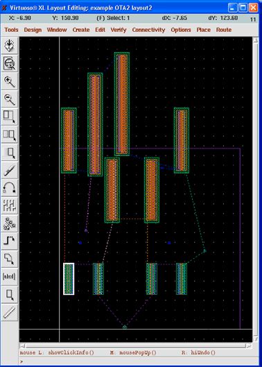
Cadence Design Environment

                                                               CONTENTS

1. INTRODUCTION........................................................................................................4
2. ANALOG IC DESIGN FLOW AND REQUIRED TOOLS....................................4
3. SETTING YOUR UNIX ENVIRONMENT..............................................................5
4. RUNNING CADENCE................................................................................................6
5. ANALOG DESIGN WITH CADENCE DESIGN FRAMEWORK II....................8
     5.1. Library Creation and Selection of Technology........................................................8
     5.2. Schematic Entry with Composer..............................................................................9
           5.2.1.      Symbol Creation........................................................................................11
     5.3. Simulation..............................................................................................................13
           5.3.1.      Setting simulator.......................................................................................14
           5.3.2.      Setting models...........................................................................................14
           5.3.3.      Setting design variables............................................................................14
           5.3.4.      Selecting the analysis................................................................................15
           5.3.5.      Running the simulation.............................................................................15
           5.3.6.      Plotting the simulation results...................................................................15
     5.4. Layout.....................................................................................................................17
           5.4.1.      Basic Full-Custom Layout........................................................................20
           5.4.2.      Full custom layout using pcells................................................................29
           5.4.3.      Fill-custom layout using Virtuoso XL.......................................................31
           5.4.4.      Hierarchical layout....................................................................................33
     5.5. Verification............................................................................................................33
           5.5.1.      Design Rule Check (DRC)........................................................................33
           5.5.2.      Layout versus Schematic (LVS)...............................................................35
     5.6. Post-Layout simulation..........................................................................................39
6. TRANSFER TO FOUNDRY.....................................................................................40
7. PRINTING IN CADENCE........................................................................................42
8. REFERENCES...........................................................................................................45

                                             APPENDIX: ADVANCED TOPICS

A.1. TRANSITION GUIDE FROM TANNER TOOLS TO CADENCE...............................47
A.2. INTRODUCTION TO SKILL......................................................................................50
A.3. LOGIC SIMULATION WITH VERILOG....................................................................52

                                                                         3
Cadence Design Environment

1. INTRODUCTION

This manual is intended to introduce microelectronic designers to the Cadence Design
Environment, and to describe all the steps necessary for running the Cadence tools at the Klipsch
School of Electrical and Computer Engineering.

Cadence is an Electronic Design Automation (EDA) environment that allows integrating in a single
framework different applications and tools (both proprietary and from other vendors), allowing to
support all the stages of IC design and verification from a single environment. These tools are
completely general, supporting different fabrication technologies. When a particular technology is
selected, a set of configuration and technology-related files are employed for customizing the
Cadence environment. This set of files is commonly referred as a design kit.

It is not the objective of this manual to provide an in-depth coverage of all the applications and tools
available in Cadence. Instead, a detailed introduction to those required for an analog designer, from
the conception of the circuit to its physical implementation, is provided. References to other
manuals and information sources with a deeper treatment of these and other Cadence tools are also
provided.

2. ANALOG IC DESIGN FLOW AND REQUIRED TOOLS

Fig. 1 shows the basic design flow of an analog IC design, together with the Cadence tools required
in each step.

First, a schematic view of the circuit is created using the Cadence Composer Schematic Editor.
Alternatively, a text netlist input can be employed.

Then, the circuit is simulated using the Cadence Affirma analog simulation environment. Different
simulators can be employed, some sold with the Cadence software (e.g., Spectre) some from other
vendors (e.g., HSPICE) if they are installed and licensed.

Once circuit specifications are fulfilled in simulation, the circuit layout is created using the Virtuoso
Layout Editor.

The resulting layout must verify some geometric rules dependent on the technology (design rules).
For enforcing it, a Design Rule Check (DRC) is performed. Optionally, some electrical errors (e.g.
shorts) can also be detected using an Electrical Rule Check (ERC). Then, the layout should be
compared to the circuit schematic to ensure that the intended functionality is implemented. This can
be done with a Layout Versus Schematic (LVS) check. All these verification tools are included in
the Diva software in Cadence (more powerful Cadence tools can also be available, like Dracula, or
Assura in deep submicron technologies).

Finally, a netlist including all layout parasitics should be extracted, and a final simulation of this
netlist should be made. This is called a Post-Layout simulation, and is performed with the same
Cadence simulation tools.

Once verified the layout functionality, the final layout is converted to a certain standard file format
depending on the foundry (GDSII, CIF, etc.) using the Cadence conversion tools.

                                                   4
Cadence Design Environment

                  Specifications

                                                     CADENCE TOOL

                Schematic Entry                       Composer

                  Simulation                          Affirma (Spectre, Hspice, cdsSpice)

           No
                      OK?

                   Yes

                 Layout Design                        Virtuoso

                    Layout
                                                      Diva (or Dracula)
                  Verification

           No
                        OK?

                   Yes

                  Post-Layout
                  Simulation                          Affirma (Spectre, Hspice, cdsSpice)

           No
                      OK?

                  Yes

          Format conversion (GDSII,
             CIF, CALMA, etc.)

                   Fabrication

                 Measurements

                   Figure 1. Analog IC design flow and Cadence tools involved

                                               5
Cadence Design Environment

3. SETTING YOUR UNIX ENVIRONMENT

Cadence can be run only on Unix terminals or PCs loaded with Linux (or Unix terminal emulators)
and X Windows servers like Exceed, X-Win32, or Xfree (Linux). Also the VNC software can be
employed (see the accompanying document about VNC tools). You need to have a tesla account. If
you are using Unix emulators, you can remote logon to the host tesla.nmsu.edu using the SSH
protocols. It your emulator does not support SSH connections, you can first start a telnet session to
gauss, and then connect to tesla with SSH. Before you can start Cadence, there are a few
configuration files that are needed in your home directory. These files determine the environment in
which Cadence runs, what libraries are to be included in your current session, etc. No doubt these
files can be edited to suit personal preferences. The setup given below is tailored for tesla (the
machine hosting the Cadence environment at the Department), and for the NCSU Design Kit. This
kit can be freely obtained from the North Carolina State University, and provides all the necessary
technology files and simulation models for using several technologies available through MOSIS.

Once in tesla, if this is the first time that you are going to use Cadence, copy the required setup files
(.cdsinit, .cdsenv, .cdsplotinit, .simrc) and scripts (runNCSU) from the directory
/Kits/NCSU/newuser. You can use the following commands, from your home directory (remember
that the Unix commands are case sensitive):

        Bash-2.05a$ cp /Kits/NCSU/newuser/.cds* .
        Bash-2.05a$ cp /Kits/NCSU/newuser/.simrc .
        Bash-2.05a$ cp /Kits/NCSU/newuser/runNCSU .

It is also recommended that this first time you create a new directory for working with Cadence, so
that all the files generated by Cadence will be in that directory. This will be your Cadence working
directory in all subsequent sessions, and you will start Cadence from there. E.g., you can type:

        Bash-2.05a$ mkdir cadence

The next step is to enter the directory where you work with Cadence, for instance:

        Bash-2.05a$ cd cadence

Before running Cadence, you have to instruct tesla so that the Cadence windows can be displayed
in your PC. You can type:

        Bash-2.05a$ DISPLAY=yourIPaddress:0
        Bash-2.05a$ export DISPLAY

where yourIPaddress means the IP address of your PC (if you don’t know it, you can get it, e.g.,
from http://www.accessam.com/myip.shtml). You can also use the DNS address.

4. RUNNING CADENCE

Once your Cadence environment setup you can start working with Cadence. You can run Cadence
from your working directory by typing:

        Bash-2.05a$ ~/runNCSU

or, equivalently, if the parent directory is your home directory,

        Bash-2.05a$ ../runNCSU

                                                   6
Cadence Design Environment
The Cadence main window (Common Interface Window, CIW) and the Library Manager
Window are opened. From the CIW menus, all Cadence main tools, online help and options can be
accessed. In the window area, all kind of messages (info, errors, warnings, etc) generated by the
different Cadence tools appear. You can also introduce commands. Fig. 2 shows this window.
Figure 2. CIW window
All the entities in Cadence are managed using libraries, and each library contains cells. Each cell
contains different design views (the structure is similar –and physically corresponds - to a directory
(library) containing subdirectories (cells), each one containing files (views). Thus, for instance, a
certain circuit (e.g. an ADC) can be stored in a library, and such library can contain the different
ADC blocks (comparators, registers, resistor strings, etc) stored as cells. Each block (cell) contains
different views (schematic, layout, etc.).
There are usually three types of libraries:
• A set of common Cadence libraries that come with the Cadence software (containing basic
components, such as voltage and current sources, R, L, C, etc).
• Libraries that come with a certain design kit and that are related to a certain technology
(e.g. transistors with a certain model attached, etc). In the NCSU design kit, some general
Cadence libraries are customized and converted into design kit libraries.
• User libraries; where the user stores its designs. These designs employ components from
the Cadence/design kit libraries.
All the libraries are managed from the Library Manager Window (shown in Fig. 3). It appears by
default at Cadence start, and can be opened at any time by selecting Tools>Library Manager...
from the CIW. Libraries with names starting by NCSU are design kit libraries, and contain basic
components for building designs. In Fig. 3, they are:
• NCSU_Analog_Parts: contains all the required blocks for designing an analog schematic
(sources, GND and VDD terminals, transistors, R, L, C, diodes, etc.)
• NCSU_Digital_Parts: similarly, it contains all parts required for digital design (logic gates,
muxes, etc.)
• NCSU_Sheets_8ths: it contains informative sheet borders for the schematics, in different sheet
sizes. Its use is optional, for design documentation.
• NCSU_TechLibAMI06: it is a technology-specific library that is created when the user attaches
this particular technology (AMI06) to a user library.
7Cadence Design Environment
Figure 3. Library Manager window
5. ANALOG DESIGN WITH CADENCE DESIGN FRAMEWORK II
Now we are going to illustrate how to carry out the complete design flow shown in Fig. 1 using the
Cadence tools. A simple Operational Transconductance Amplifier (OTA) will be designed in the
AMI 0.5µm CMOS technology. However, the same procedures apply to complete chip designs.
5.1. Library creation and selection of technology
It is recommended that you use a library to store related cell views; e.g., use a library to hold all the
cell views for a single project (that can involve a complete chip design). In our example, we are
going to create a new library for our design. From the CIW or from the Library Manager window,
a) Select File -> New -> Library. A new window appears (see Fig. 4).
b) Enter a library name, e.g., example.
c) Enter the absolute path name if you want the library created somewhere else than the working
directory.
d) Choose the Attach to an existing techfile option.
e) Choose your technology; for instance, for AMI 0.5µm in MOSIS, choose AMI 0.6u C5N
NOTE: The NCSU Kit 1.6u and 0.6u AMI processes correspond to MOSIS' 1.5µ and 0.5µ. For
consistency, the NCSU kit names its tech libs based on the drawn length of devices, so this
sometimes runs afoul of MOSIS' naming scheme.
8Cadence Design Environment
This will be the technology chosen for your design (that you will employ eventually for
fabrication). Now all the designs made in this library are technology-dependent (e.g., the schematic
MOS symbols have by default the model for this technology, the available layout layers correspond
to this technology, etc.).
Figure 4. Create Library window
5.2. Schematic Entry with Composer
5.2.1. Transistor-level schematic
The traditional method for capturing (i.e. describing) your transistor-level or gate-level design is via
the Composer schematic editor. Schematic editors provide simple, intuitive means to draw, to place
and to connect individual components that make up your design. The resulting schematic drawing
must accurately describe the main electrical properties of all components and their interconnections.
Also included in the schematic are the power supply and ground connections, as well as all "pins"
for the input and output signals of your circuit. This information is crucial for generating the
corresponding netlist, which is used in later stages of the design. The generation of a complete
circuit schematic is therefore the first important step of the former design flow. Usually, some
properties of the components (e.g. transistor dimensions) and/or the interconnections between the
devices are subsequently modified as a result of iterative optimization steps. These later
modifications and improvements on the circuit structure must also be accurately reflected in the
most current version of the corresponding schematic.
Now you are going to create the OTA schematic. From the CIW or from the Library Manager
window,
a) Select the library name that you just created, e.g., example.
b) Select File -> New -> Cellview
c) Enter a cell name, for instance, OTA
d) Choose Composer - Schematic as the Tool. View name should be schematic.
e) Click OK.
An empty blank Composer - schematic window should open. In this window you will create your
schematic. The final schematic is shown in Fig. 5 (the icon actions are also shown). To create it,
you can employ the window top menus or left icons (or also shortkeys). This multiple access to
9Cadence Design Environment
actions is common to all the Cadence tools. A detailed information concerning the use of the
schematic editor can be obtained by selecting Help from this window. Basically, you can:
• Create components: by selecting the Instance icon and browsing in the pop-up window through
the different libraries. Most components (transistors, R, L, C, sources, rail terminals, etc.) are in
the NCSU_Analog_Parts library. When you create an instance of a certain component (e.g.,
transistor, R, C, etc.) a window appears where you can select the properties of this element.
Note that for transistors, the model is automatically set according to the technology you have
selected, and that some parameters (drain and source area and perimeter, etc) are
automatically calculated.
NOTE: There are three-terminal (nmos, pmos) and four-terminal (nmos4, pmos4) MOS devices
available. The three-terminal devices have a hidden fourth (bulk) terminal, which is connected by
default to "gnd!" for nmos and "vdd!" for pmos. This means that you need to have nets named
"vdd!"and "gnd!" somewhere in your schematic. (The easiest way to do this is to drop in the vdd
and gnd pins from NCSU_Analog_Parts->Supply_Nets.) If you don't have these nets in your
schematic somewhere, you'll get complaints about unknown nets either in the netlister or in LVS.
(You can also change the bulk node in the three-terminal device if you want to. Just select the
device in the schematic, and bring up the "Edit Object Properties" form (Edit->Object-
>Properties...). Change the "Bulk node connection" field to whichever net you want.
• Wire components: select the Wire (narrow) icon, click to the first terminal and drag until the
other terminal, then click again.
In complex designs, for avoiding excessive wiring, labels can be employed. When two wire
ends are labeled with the same name, they are effectively connected. Labels are created, e.g.,
with the Label icon.
• Set instance properties: you can modify at any time the properties of a certain component
instance (resistance value, transistor dimensions, etc), e.g., by selecting the instance (click on it)
and then clicking on the Properties icon. You can also change a group of instances of the same
component simultaneously, by first selecting this group, then clicking in Properties and
modifying the parameters, selecting Apply to > All selected.
Most of the commands in Composer will start a mode (the default mode is selection), and as long as
you do not choose a new mode (by clicking an icon, pressing a shortkey or selecting a menu item)
you will remain in that mode. To quit from any mode and return to the default selection mode, the
"Esc" key can be used.
There are basically two ways of creating schematics:
a) Non-Hierarchical schematic. You introduce all the circuit schematic at the same (transistor)
level, including the required sources. This is only viable for small designs.
b) Hierarchical schematic. If your design is very large, or if you want to reuse your design in
other designs (e.g. an OpAmp to be employed in other circuits), you should create basic blocks
at a low level, then create symbols for them and then use these symbols as basic components at
a higher hierarchical level of the design. It is the same concept employed in SPICE netlists with
the .SUBCKT command.
10Cadence Design Environment
When a certain circuit design consists of smaller hierarchical components (or modules), it is
usually very beneficial to use this approach, first identifying such modules early in the design
process and then assigning each such module a corresponding symbol (or icon) to represent that
circuit module. This step largely simplifies the schematic representation of the overall system.
The "symbol" view of a circuit module is an icon that stands for the collection of all
components within the module.
A symbol view of the circuit is also recommended for some of the subsequent simulation steps;
thus, the schematic capture of the circuit topology is usually followed by the creation of a
symbol to represent the entire circuit. The shape of the icon to be used for the symbol may
suggest the function of the module (e.g. logic gates - AND, OR, NAND, NOR), but the default
symbol icon is a simple rectangular box with input and output pins. Note that this icon can now
be used as the building block of another module, and so on, allowing the circuit designer to
create a system-level design consisting of multiple hierarchy levels.
This is the approach that will be followed in our example. For doing this, we have to create a
symbol view of our OTA.
5.2.2. Symbol Creation
a) First, you have to create pins in your schematic in those non-global nets (inputs, outputs,
supplies perhaps) that have to be accessible outside the symbol. For doing this, you can select
the Create Pin icon in the Composer schematic window, select the pin name, its input or output
configuration, etc, and then click at the end of the wire when the pin has to be placed. Six pin
icons have been placed in the example of Fig. 5: v+, v-, ibias, vdd, vss (input pins) and out
(output pin).
b) Now, select Design > Create Cellview > From cellview. A window appears that by default
creates a symbol view from the schematic view. Just click OK. A black window pops up with
the symbol. It can be edited if desired (changing shape, pin distribution, etc.). Fig. 6 shows the
resulting symbol (after some editing) and the actions associated to the left icons.
Now you can use your design in a higher hierarchical schematic. For instance, in Fig. 7 a new
schematic is created where the OTA symbol is instantiated and some sources are included, forming
a voltage follower ready to be simulated. This will be the design that we will simulate subsequently.
For instantiating the OTA symbol, the procedure is identical than for any other component. You can
select the Instance icon, go to your library and select the OTA.
11Cadence Design Environment
Check and Save
Save
Zoom In by 2
Zoom Out by 2
Stretch
Copy
Delete
Undo
Property
Instance
Wire (narrow)
Wire (wide)
Label
Pin
Figure 5. Composer Schematic Editor window
Save
Zoom In by 2
Zoom Out by 2
Stretch
Copy
Move
Delete
Undo
Property
Pin
Line
Rectangle
Label
Selection Box
Figure 6. Symbol Editor window
12Cadence Design Environment
Figure 7. Composer Schematic Editor window, hierarchical design
We can go up and down in the hierarchy with menu options or with shortkeys X (or x, to descend)
and b (to ascend). Parameters for voltage and current sources are set as for any other component, by
selecting the instance and editing its properties.
5.3. Simulation
After the transistor-level description of a circuit is completed using the Schematic Editor, the
electrical performance and the functionality of the circuit must be verified using a Simulation tool.
The detailed transistor-level simulation of your design will be the first in-depth validation of its
operation, hence, it is extremely important to complete this step before proceeding with the
subsequent design optimization steps. Based on simulation results, the designer usually modifies
some of the device properties (such as transistor width-to-length ratio) in order to optimize the
performance.
The initial simulation phase also serves to detect some of the design errors that may have been
created during the schematic entry step. It is quite common to discover errors such as a missing
connection or an unintended crossing of two signals in the schematic. Some of these errors (e.g.,
floating nodes) can be detected even before simulation, by pressing the Check and Save icon in the
schematic window.
The second simulation phase will follow the "extraction" of a mask layout (post-layout simulation),
to accurately assess the electrical performance of the completed design.
13Cadence Design Environment
Like in other simulation environments, it is the netlist text file extracted from the schematic (or
layout) what is actually simulated.
In order to start simulations, from the Composer window that contains the schematic you want to
simulate (in our example, test_OTA, shown in Fig. 7), choose Tools > Analog Environment. The
simulation window appears (Fig. 8).
Choose design
Circuit to be
simulated Choose analysis
List of analyses to be performed Set variables
Choose outputs
Design Delete
Variables Run simulation
Stop simulation
Plot output
Figure 8. Simulation window
By default, the design from which we have launched the window can be simulated using Spectre.
5.3.1. Setting simulator
We can change the design with the corresponding icon or using the menus. We can also change the
simulator by choosing Setup->Simulator/Directory/Host and setting e.g., HSPICE. Obviously, the
chosen simulator must be installed and licensed.
5.3.2. Setting models
Also by default the component models for the library technology (in our example AMI 0.5µ) will be
used. If we want to use other models, we can store them in some directory and choose Setup-
>Model Path, typing the full path (including filename) of the model(s) needed for simulation,
before the path for the default models (list position means precedence in the search for models).
This procedure assumes that your models have the same name as the default models.
5.3.3. Setting design variables
We can use in our schematic design variables for the component parameters, so that their values can
be assigned just before simulation. For instance, we can name some (or all) of the transistor lengths
as ‘L’. Then, in the simulation window we assign the desired value to L. This way, we can make
several simulations just changing the parameter(s) without having to edit the schematic. For editing
design variables, choose Variables >Edit (or select the corresponding icon).
14Cadence Design Environment
5.3.4. Selecting the analysis
Several analyses can be performed (DC, AC, transient, etc.). For selecting the required analysis,
choose Analysis > Choose (or the corresponding icon) and complete the settings in the window that
appears.
Example: Transient analysis, choose 'tran', ‘conservative’ and then type in the total time you wish
to run (ex. 40n or 40e-9)
Currents cannot be plotted by default. If you are interested in viewing currents in your circuit,
choose: Output > Save all ....> Select all DC/transient terminal currents (for DC and transient
analyses) or Select all AC terminal currents (for AC analysis).
5.3.5. Running the simulation
When the former steps are performed, simulation can start. Click the Green Traffic Light Icon
(bottom right corner of the simulation window) or choose Run > Simulation to run the simulation.
If you want to interrupt the simulation at any instant, click the Red Traffic Light Icon or choose
Run > Interrupt.
5.3.6. Plotting the simulation results
There are different ways of plotting the results of a simulation. Here we are going to use the
Calculator tool. After running the simulation, choose Tools > Calculator. A calculator window
appears (see Fig. 9).
Figure 9. Calculator
With this tool we can, among other things:
• Plot in a waveform window the different currents and voltages
• Print (to a printer or a file) the selected waveforms
• Perform different functions on the selected waveform (multiply, divide, dB calculation,
DFT, THD calculation, bandwidth, maximum and minimum calculation, etc).
• Use as a normal calculator for making calculations
You can select the Help option for details.
15Cadence Design Environment
When we want to display a certain waveform, we first select the button corresponding to the type of
waveform. The most common are:
Vt: nodal voltage (transient analysis)
It: terminal current (transient analysis)
Vf: nodal voltage (AC analysis)
If: terminal current (AC analysis)
Vs: nodal voltage (DC sweep)
Is: terminal current (DC sweep)
Vdc: nodal voltage (quiescent value)
Idc: terminal current (quiescent value)
Then, we just click on the corresponding wire (voltages) or terminal (currents) in the schematic.
Finally, we select in the calculator:
Plot: To plot the waveform without removing already displayed waveforms
Erplot: To remove displayed waveforms and plot the selected one.
The waveform is plotted in the Waveform Window. We can continue selecting circuit nodes and
selecting plot or erplot. Finally, press Esc for disabling the current action.
The Waveform Window, showing the input and output voltages of our voltage buffer, is shown in
Fig. 10. Different configurations can be chosen (various graphs or axes, cursors, etc.). Press the
Help button for details.
If you want to modify and re-simulate your circuit, just change your schematic, design variables or
simulation command, run again the simulation and select Window > Update results in the
Waveform Window.
Figure 10. Waveform window
16Cadence Design Environment
5.4. Layout
The creation of the mask layout is one of the most important steps in the full-custom (bottom-up)
design flow, where the designer describes the detailed geometry and the relative positioning of each
mask layer to be used in actual fabrication, using a Layout Editor. Physical layout design is very
tightly linked to overall circuit performance (area, speed and power dissipation) since the physical
structure determines the transconductances of the transistors, the parasitic capacitances and
resistances, and obviously, the silicon area that is used to realize a certain function.
The physical (mask layout) design is an iterative process, which starts with the circuit topology and
the initial sizing of the transistors. It is extremely important that the layout design must not violate
any of the Layout Design Rules of the fabrication process, in order to ensure a high probability of
defect-free fabrication of all features described in the mask layout. It is also important to Extract
the netlist underlying the layout view, for two main purposes:
• This allows comparing it with the netlist extracted from the schematic. This Layout versus
Schematic (LVS) comparison ensures that the layout actually implements the required
functionality.
• If the extraction program allows to extract also parasitics from the layout view, a more accurate,
Post-Layout Simulation, can be performed taking into account the geometry of the circuit.
The detailed mask layout requires a very intensive and time-consuming design effort, so that
automated tools are employed as much as possible. Typically, the design of digital circuits based on
single-clock synchronous logic is completely automated. First, a circuit description (typically in a
HDL language as VHDL or Verilog) is synthesized, leading to a gate-level circuit description. From
this gate-level netlist, Place&Route programs generate automatically the layout.
Unfortunately, analog circuits are very sensitive to the layout style, so that an automated procedure
is difficult to implement. Usually a tedious, full-custom approach is followed, where the designer
builds manually the layout, basically drawing rectangles of different layers. Nevertheless, there are
some aids to the full-custom designer:
• Parametrized Cells (Pcells). They are complete layout cells (e.g. a transistor or a row of
contacts) already available, containing all the required layers, and whose characteristics can
be set by the designer by means of some parameters (e.g., transistor length or width, etc.).
They can be implemented in Cadence using the SKILL language, and some of them come
usually with a certain Design Kit.
• Standard Cells. Cells already designed that can be placed in our layout. In case of digital
cells, they are usually automatically placed with a Place&Route program.
The availability of parametrized and standard cells in a certain Design Kit is an important
factor for its quality (and price!).
• “Semi-automated” layout. The layout of the components in the schematic is automatically
generated from the schematic, with its corresponding sizes. The designer just places and
routes such components. Even for assisting place and route tasks there are additional
features available. This can be done in Cadence with the Virtuoso Accelerator (Virtuoso
XL).
We will now make the layout of our OTA. From the CIW or from the Library Manager window,
a) Select the library name that you just created, e.g., example.
b) Select File -> New -> Cellview
17Cadence Design Environment
c) Enter the cell name, e.g., OTA
d) Choose Virtuoso as the Tool. View name should be layout.
f) Click OK. Two design windows will pop up (see Fig. 11), LSW and Virtuoso Editor.
LSW
The Layer Selection Window (LSW) lets the user select different layers of the mask layout.
Virtuoso will always use the layer currently selected in the LSW for editing. The LSW can also be
used to restrict the type of layers that are visible or selectable. To select a layer, simply click on the
desired layer within the LSW.
WARNING: Only layers with the dg property will be fabricated. The rest are basically for
labeling, highlighting errors, and documenting!!
• Common Layers. The following layers are common to all MOSIS CMOS processes:
NCSU Kit Stream layer CIF layer
Description
layer name number abbreviation
nwell N-well 42 CWN
pwell P-well 41 CWP
active active (diffusion) 43 CAA
nactive* N-active 43 CAA
pactive* P-active 43 CAA
nselect N-select (ion implant) 45 CSN
pselect P-select (ion implant) 44 CSP
poly polysilicon 46 CPG
metal1 first-layer metal 49 CMF
ca metal1-active contact (obsolete; use cc instead) 48 CCA
metal1-polysilicon contact (obsolete; use cc
cp 47 CCP
instead)
cc generic contact (metal1 to active or polysilicon) 25 CCC
via metal1-metal2 contact 50 CVA
metal2 second-layer metal 51 CMS
pad wirebond pad marker 26 XP
glass overglass cut 52 COG
cap_id capacitor marker NA NA
res_id resistor marker NA NA
dio_id diode marker NA NA
*
nactive and pactive are simply convenience layers for the user, not mask layers, and are treated as
``active'' for purposes of streaming out, DRC, and extraction.
Table I. Common layers in all MOSIS processes
• Layers corresponding to optional technology features. Some specific additional layers can
be included for implementing optional features of the technology. Table II shows which active
processes support which optional technology features. Table III shows the mask layers that
correspond to the technology features.
18Cadence Design Environment
Technology AMI AMI HP HP TSMC 0.4um TSMC 0.4um TSMC TSMC
Feature 1.6um 0.6um 0.6um 0.4um (4M) (4M2P) 0.3um 0.2um
electrode
poly capacitor
high-res implant
npn
third-layer metal
fourth-layer metal
fifth-layer metal
sixth-layer metal
metal-metal cap
silicide block
thin-oxide cap
high-voltage
FETs
Table II. Optional features in some MOSIS processes
Technology CDK layer Stream layer CIF layer
Description
Feature names number abbreviation
elec second polysilicon 56 CEL
electrode metal1-electrode contact (obsolete; use
ce 55 CCE
cc instead)
poly capacitor polycap lower poly for thin-oxide capacitor 28 CPC
high-res
highres implant for high-resistance elec (poly2) 34 CHR
implant
pbase base for vertical NPN transistors 58 CBA
npn *
cactive marker for collector of NPN transistors 43 CAA
third-layer metal3 third metal 62 CMT
metal via2 metal2-metal3 contact 61 CVS
fourth-layer metal4 fourth metal 31 CMQ
metal via3 metal3-metal4 contact 30 CVT
fifth-layer metal5 fifth metal 33 CMP
metal via4 metal4-metal5 contact 32 CVQ
sixth-layer metal6 sixth metal 37 CM6
metal via5 metal5-metal6 contact 36 CV5
metal-metal
metalcap inter-metal layer for capacitor 35 CTM
cap
silicide block sblock silicide implant block for resistor 29 CSB
well implant for linear thin-oxide
thin-oxide cap cwell 59 CWC
capacitor
high-voltage
tactive thick oxide 60 CTA
FETs
*
cactive is simply a convenience layer for the user, not a mask layer, and is treated as ``active'' for
purposes of streaming out, DRC, and extraction.
Table III. Additional layers supporting the optional features
19Cadence Design Environment
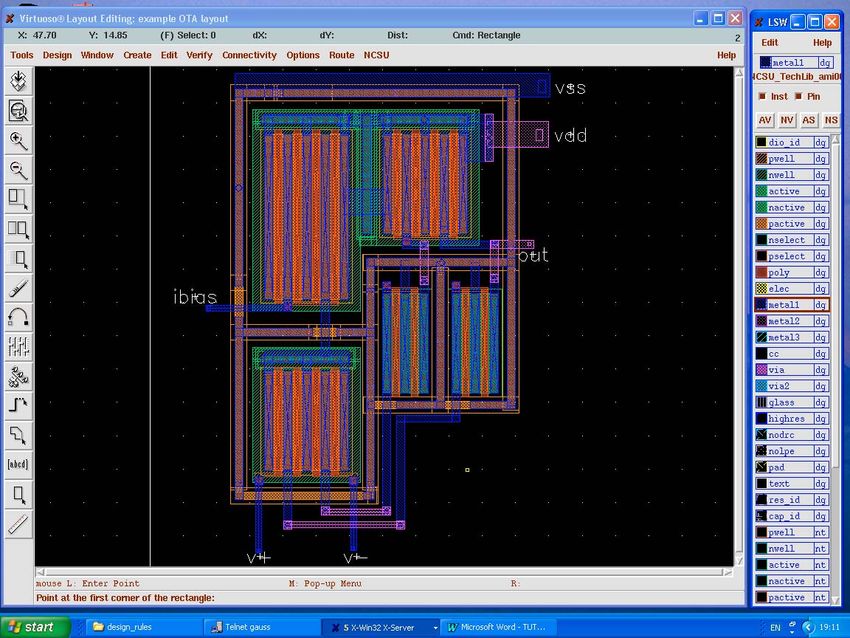
Virtuoso
Virtuoso is the main layout editor of Cadence design tools. There is a small (icon) button bar on the
left side of the editor. Commonly used functions can be accessed pressing these buttons. There is an
information line at the top of the window. This information line, (from left to right) contains the X
and Y coordinates of the cursor, number of selected objects, the traveled distance in X and Y, the
total distance and the command currently in use. This information can be very handy while editing.
At the bottom of the window, another line shows what function the mouse buttons have at any given
moment. Note that these functions will change according to the command you are currently
executing.
Info. Line
Save
Fit Edit
Zoom In by 2
Zoom Out by 2
Stretch
Copy
Move
Delete
Undo
Property
Instance
Path
Polygon
Label
Rectangle
Ruler
Mouse
Function
Next
Action
Figure 11. Virtuoso and LSW windows
Similarly to Composer, most of the commands in Virtuoso will start a mode (the default mode is
selection), and as long as you do not choose a new mode you will remain in that mode. To quit from
any mode and return to the default selection mode, the "Esc" key can be used.
As mentioned before, we can do the layout of our OTA (such as that shown in Fig. 11) following
different degrees of automation. The following section illustrates them.
5.4.1. “Basic” Full-Custom layout
The layout is made layer by layer, in any order. This is similar to the mask layout edition in Magic
or L-Edit. In Cadence, this is not usually done in practice (unless the Layout Editor/Design Kit do
not support more advanced methods). This is included here as a reference, you can skip this section
and go to the more practical approaches of Sections 5.3.2 and 5.3.3.
20Cadence Design Environment
Additional details are provided in the Cadence Online Help, and in the following tutorial:
http://turquoise.wpi.edu/cds/
In our example the technology selected is n-well, so that the black area represents the p substrate.
The full custom layout process consist basically on repeatedly selecting a certain layer from the
LSW window, choosing the Rectangle icon to create a rectangle and drawing it.
As mentioned above, the geometries (enclosure, extension, minimum dimensions, etc) of the objects
created have to comply with a set of rules dependent on the technology, named Design Rules. Once
your layout completed, a Design Rule Check (DRC) is performed to enforce this point. Object
dimensions can be checked by observing the screen coordinates or using the ruler (Ruler icon or k
shortkey).
- For designing a PMOS transistor of aspect ratio W/L (the order of layer drawing is irrelevant):
Since we are using an n-well process, the substrate will be p-substrate. To create a
PMOS transistor we need an n-well in which the transistor will be formed.
• Draw the well
a) Select the n-well layer from the LSW window
b) Select the Create->Rectangle (or choose the Rectangle icon from
the side toolbar).
c) Using your mouse, draw the n-well with the size required.
• Draw the p- and n-select regions for the p transistor
a) Select the pselect layer from the LSW window; we will draw the
pselect enclosing the transistor
b) Select the Create->Rectangle (or choose the Rectangle icon from
the side toolbar).
c) Using your mouse, draw the pselect on the cellview. The pselect
should be placed within the n-well (you can use the Edit->Move
command to move the layer) with geometry according to the
Design Rules.
• Draw Diffusions
a) Select the pactive layer from the LSW window; we will draw the
active region of the p-device
b) Select the Create->Rectangle (or choose the Rectangle icon from
the side toolbar).
c) Using your mouse, draw the pactive on the cellview (it should be
enclosed by the pselect and by the nwell, as determined by the
Design Rules). Its width should be W, and its length as small as
possible, for reducing device parasitics.
NOTE: In many SCMOS processes there are 3 active layers: active, nactive and pactive. They are
interchangeable since they translate to the same physical layer in fabrication. As mentioned in
Table I, nactive and pactive layers are provided for differentiating graphically n and p acive
diffussions (assigning them different colors) but what makes an active layer of type n or p is the
nselect or pselect layer, respectively, surrounding it).
21Cadence Design Environment
• Draw Poly
a) Select the poly layer from the LSW window
b) Select the Create->Rectangle (or choose the Rectangle icon from
the side toolbar).
c) Using your mouse, draw the poly on the cellview
The poly should be placed at the center of the p-island, with length
L, and should extend over the p-island as specified in the Design
Rules.
• Place Contacts
a) Select the contact layer from the LSW window
b) Select the Create->Rectangle (or choose the Rectangle icon from
the side toolbar).
c) Using your mouse, draw the contact on the cellview. Most
technologies require one (or two) fixed contact size/s.
Contacts should be placed at both sides of the pactive. You can
copy the generated contact throughout the drain and source areas.
The number of contacts should be as large as possible. Their size is
determined by the corresponding Design Rules.
- For designing a NMOS transistor of dimensions W/L (the order of layer drawing is irrelevant):
• Draw the nselect
a) Select the nselect layer from the LSW window
b) Select the Create->Rectangle (or choose the Rectangle icon from
the side toolbar).
c) Using your mouse, draw the nselect on the cellview
• Draw the N active region
a) Select the nactive layer from the LSW window
b) Select the Create->Rectangle (or choose the Rectangle icon from
the side toolbar).
c) Using your mouse, draw the nactive on the cellview ; it should be
enclosed by the nselect (as determined by the Design Rules). Its
width should be W, and its length as small as possible.
• Draw Poly
a) Select the poly layer from the LSW window
b) Select the Create->Rectangle (or choose the Rectangle icon from
the side toolbar).
c) Using your mouse, draw the poly on the cellview
The poly should be placed at the center of the n-island, with length
L, and should extend over the n-island as specified in the Design
Rules.
• Place Contacts
a) Select the contact layer from the LSW window
b) Select the Create->Rectangle (or choose the Rectangle icon from
the side toolbar).
22Cadence Design Environment
c) Using your mouse, draw the contact on the cellview. Most
technologies require one (or two) fixed contact size/s.
Contacts should be placed at both sides of the nactive. You can
copy the generated contact throughout the drain and source areas.
The number of contacts should be as large as possible. Their size is
provided by the corresponding Design Rules.
- Designing resistors:
Integrated resistors can be made by different layers (diffusion, well, poly). In analog
applications linear resistors are usually required, so that they are typically implemented
using poly, and if technology allows, using a special high resistive poly layer.
The procedure for designing a resistor is as follows:
a) Determine the number of squares required by the resistor
geometry:
Resistor Value(Ω )
No. squares =
Sheet Resistance(Ω / square )
Typical sheet resistances are 20-30 Ω/ for (silicide) poly and
about 1 kΩ/ for the high-resistive poly.
b) Choose the width W of the resistor strip. It should be larger than
the minimum given by the Design Rules for fabricating resistors.
c) Obtain the length L of the resistor strip: L= W x No. Squares.
d) If L is too long, several bends can be introduced (thus forming
serpentine resistors). Recalculate (b) counting about ½ square for
each bend corner.
- Poly1 resistor:
• Draw Poly
a) Select the poly layer from the LSW window
b) Select the Create->Rectangle (or choose the Rectangle icon from
the side toolbar).
c) Using your mouse, draw the poly on the cellview of width W and
length slightly larger than L. (for allowing contacts at the resistor
ends)
• Place Contacts
a) Select the contact layer from the LSW window
b) Select the Create->Rectangle (or choose the Rectangle icon from
the side toolbar).
c) Using your mouse, draw the contact on the extremes of the poly
strip.
23Cadence Design Environment
• Identify the device as a resistor
If the Design Kit does not extract resistances by default (as the AMI
technologies in the NCSU Kit) a layer is provided to identify where a
resistor is, and to obtain its resistance value during netlist extraction. It
our example technology, it is res_id (this layer is not fabricated).
a) Select the res_id layer from the LSW window
b) Select the Create->Rectangle (or choose the Rectangle icon from
the side toolbar).
c) Using your mouse, draw a rectangle of length L limited by the
contacts and surrounding the resistor (according to the Design
Rules).
Fig. 12 shows an example of a poly resistor, of 6 squares. Its
approximate value is therefore 6 x (20-30 Ω/ ) = 120 – 180 Ω
Poly
Metal 1 Metal 1
Res_id
Figure 12. Poly resistor
- High-Res resistor:
Some technologies offer a highly resistive polysilicon layer, useful in
analog design for obtaining linear resistors of large values using small
silicon area. Usually they are made using the poly layer (more precisely,
one of the poly layers if technology has two) and an additional layer that
provides the high resistance properties.
The procedure for the AMI 0.5µ technology is as follows
• Draw Poly
a) Select the elec layer from the LSW window (this is the second
poly layer in this process)
b) Select the Create->Rectangle (or choose the Rectangle icon from
the side toolbar).
c) Using your mouse, draw the poly on the cellview of width W and
length slightly larger than L. (for allowing contacts at the resistor
ends).
• Place Contacts
a) Select the contact layer from the LSW window
b) Select the Create->Rectangle (or choose the Rectangle icon from
the side toolbar).
c) Using your mouse, draw the contact on the extremes of the poly
strip.
24Cadence Design Environment
• Identify the device as a high-resistance resistor
a) Select the high_res layer from the LSW window
b) Select the Create->Rectangle (or choose the Rectangle icon from
the side toolbar).
c) Using your mouse, draw a rectangle of length L, separated from the
contacts and surrounding the resistor (according to the Design
Rules).
Fig. 13 shows an example of a poly resistor, of 6 squares. Its
approximate value is therefore 6 x (1kΩ/ ) = 6 kΩ
Elec
Metal 1 Metal 1
High_res
Figure 13. Hig-res resistor
NOTE: Fabricated resistance values can differ considerably from
calculations. Therefore, the operation of a design should NEVER
rely on exact resistance values, but on resistance RATIOS.
- Other resistor:
Resistors can also be made using diffusion or n-well layers, but the
resulting resistances are strongly nonlinear and temperature-dependent,
so that their application in analog design is marginal. The layout is very
similar to that described for poly resistors, substituting the poly layer
by the proper layer. The resistor_id layer should be present for
extracting these resistances in the layout netlist.
- Designing capacitors:
Capacitors in analog circuits need typically be linear. Hence they are
usually made (if technology provides a second poly layer) using two
overlapping poly regions (poly1 and poly2) with a thin oxide layer in
between. The overlapping region defines the required capacitance.
When two poly layers are available, the first poly layer (gate of MOS
transistors and bottom plate of capacitors) is usually called poly or
poly1. The second poly layer (top plate of capacitors and sometimes
layer for resistors) is called polycap or poly2 or elec.
The procedure for designing a poly-poly capacitor is as follows:
a) Determine the area required by the capacitor geometry:
Capacitor Value(F )
Area(µm 2 ) =
Capacitance per unit area (F / µm 2 )
25Cadence Design Environment
Typical poly-poly capacitances per unit area are 0.5 – 1 fF/µm2. For the
AMI 0.5µ process, it is approximately 0.9 fF/µm2.
• Draw elec
a) Select the elec layer from the LSW window (this is the second
poly layer in this process)
b) Select the Create->Rectangle (or choose the Rectangle icon from
the side toolbar).
c) Using your mouse, draw a rectangle with the area calculated
previously.
• Draw poly
a) Select the poly layer from the LSW window
b) Select the Create->Rectangle (or choose the Rectangle icon from
the side toolbar).
c) Using your mouse, draw a rectangle overlapping the previous elec
geometry according to the Design Rules.
• Place Contacts
a) Select the contact layer from the LSW window
b) Select the Create->Rectangle (or choose the Rectangle icon from
the side toolbar).
c) Using your mouse, draw the contact on the top and bottom
capacitor plates, according to the Design Rules.
Fig. 14 shows a poly capacitor in the AMI 0.5µ process.
Elec
Poly
Figure 14. Poly-Poly capacitor
NOTE 1: The geometry of the capacitor need not be a rectangle. It
can fit the layout geometry in order to minimize area. In any case, if
matched capacitors are required, they should not only have the same
area but also the same geometry.
26Cadence Design Environment
NOTE 2: Fabricated capacitor values may differ considerably from
calculations. Therefore, the operation of a design should NEVER
rely on exact capacitance values, but on capacitance RATIOS.
- Layout: necessary connections:
• Draw the well-contacts
a) Select the nselect layer from the LSW window; we will draw the
nselect enclosing the n-well contact for the PMOS transistors.
b) Select the Create->Rectangle (or choose the Rectangle icon from
the side toolbar).
c) Using the mouse, draw the nselect on the cellview; If technology
allows, the nselect can abut directly to the pselect of the PMOS
transistor, but they should not overlap. Also, both selects should be
placed within the n-well.
d) Select the nactive layer from the LSW window; we will draw the
body contact region of the P devices.
e) Select the Create->Rectangle (or choose the Rectangle icon from
the side toolbar).
f) Using your mouse, draw the nactive on the cellview
g) Add contacts in the well-contact island.
• Draw the Substrate-contacts
a) Select the pselect layer from the LSW window; we will draw the
pselect enclosing the substrate contact for the NMOS transistors
b) Select the Create->Rectangle (or choose the Rectangle icon from
the side toolbar).
c) Using the mouse, draw the pselect on the cellview; If technology
allows, pselect abuts directly to the nselect of the NMOS transistor,
but they should not overlap.
d) Select the pactive layer from the LSW window
e) Select the Create->Rectangle (or choose the Rectangle icon from
the side toolbar).
f) Using your mouse, draw the p-island on the cellview.
g) Add contacts in the substrate-contact island.
• Metal Connections
a) Connect the transistor terminal contacts, terminal contacts of
capacitors and resistors, and substrate/well contacts using the
Metal1 layer (gates can be connected directly using the Poly1
layer).
b) For interconnections, you can use any metal layer provided by the
technology (Metal1, Metal2, Metal3, ...) so that metal paths can
cross without being shorted. In two-metal technologies, usually one
metal tends to be used for the horizontal paths and other for the
vertical ones.
27Cadence Design Environment
- Additional steps for layout verification
• Add Pins:
Once you have finished creating the layout, the next step is to add the I/O pins of your
circuit. It is necessary to add the vdd! and vss! (or gnd!) pins to your circuit for the purpose
of verification (if you have used these terminals in the schematic). Net labels ending in ‘!”
mean global nodes (i.e., all wires in the entire design hierarchy labeled with this name are
considered to be connected, even if they physically are not. They are usually power nets).
The following is a procedure for adding I/O pins to your circuit:
From your Layout window:
1. Choose Create->Pin... from the menu. The Create Pin form will appear
(Fig. 15).
2. If the form is titled "Create Shape Pin", choose "sym pin" under the Mode
option.
3. Enter a TerminalName(the name of your pin).
4. Make sure that the "Display Pin Name" option is selected.
5. Specify the "I/O Type" as input, output, or inputoutput, according to the
schematic.
6. Specify the Pin Type as Metal1, Metal2,... depending on which is the top
layer at the place that the pin is to be inserted (they should match).
7. Specify the Pin Width to the desired pin width (the pin is square).
8. Move the mouse to specify where the pin and the label should be placed.
Figure 15. Create Pin window
In our example, you need to add pins for the input terminals (named in our OTA example v+, v-),
outputs (out),ibias, vdd, and vss. This information will be employed for the extraction of the netlist
from the layout and subsequent comparison with the schematic netlist. Therefore, pin names in
layout and schematic must mach perfectly (comparison is case sensitive).
28Cadence Design Environment
5.4.2. Full-Custom Layout using pcells
The above approach is useful for learning the design rules and layers available for a certain
technology, but it is not usually followed (if one can avoid it). Instead, basic elements (transistors,
resistances, capacitors, etc) can be directly created using parametrized cells (pcells), by defining
their dimensions in a Properties window. Properties of a certain pcell can be modified after creation
by selecting the pcell and clicking on the Property icon.
- For designing a PMOS transistor of aspect ratio W/L:
Select the Instance NCSU_TechLib_ami06 > pmos. In the Create Instance window (Fig.
16), you can select the desired W and L. Then, place the pcell.
For creating cascoded or interdigitized structures (e.g., for current mirrors or differential
pairs) it is useful to use the Multiplier or Finger fields in the instance properties. They
generate multiple instances of the transistor, sharing the adjacent instances a common (drain
or source) terminal with metal contacts (Multiplier) or without them (Finger).
Figure 16. Creating a PMOS transistor
- For designing an NMOS transistor:
Similar to the PMOS, just select the Instance NCSU_TechLib_ami06 > nmos.
- For designing resistances and capacitances:
Similar to the procedure described in the former section for the AMI 0.5µ process (other
processes may include resistor and capacitor pcells). However, pcells can be employed for the
required poly contacts. There are also two rudimentary pcells for poly resistances,
(NCSU_TechLib_ami06 > res (wide) or res2 (thin)), but they are not very useful.
29Cadence Design Environment
- Creating contacts:
Select Create > Contact, then select the type of contacts and the number of contacts
required in the pop-up window (Fig. 17). The types of contacts available in the AMI 0.5µ
process are:
• M1-P: Metal1-Pactive contact. Used mainly in PMOS drain and source contacts,
substrate contacts.
• M1-N: Metal1-Nactive contact. Used mainly in NMOS drain and source contacts.
• NTAP: Metal1-Nwell contact. Used in N-well contacts.
• M1-POLY: Metal1-Poly contact. Used mainly in gate transistors and poly resistor
terminals.
• M1-ELEC: M1 to poly2 contact. Used mainly in top plate contacts of poly-poly
capacitors and in “high-res” resistor terminals.
• M1-M2: Metal1-Metal2 via.
• M2-M3: Metal2-Metal3 via.
Figure 17. Creating a contact
- Routing:
Metal and poly paths can be created using the Create > Rectangle function. Alternatively,
they can be made using the Path icon (or Create Path, or p shortkey). You select the path
width and draw the path. Orthogonal or diagonal paths can usually be created. Moreover,
you can create a via and change the metal layer without quitting the Path function, using
Change to layer .. in the Create Path window. This tool is extremely necessary for wiring
large paths in the highest hierarchies of the layout.
The Path tool is also very useful for creating serpentine resistors.
- Pins:
They are created as explained in the above section.
30You can also read