Versal ACAP PCB Design - User Guide - Xilinx
←
→
Page content transcription
If your browser does not render page correctly, please read the page content below
Versal ACAP PCB Design

User Guide
UG863 (v1.2) February 1, 2022

Xilinx is creating an environment where employees, customers, and
partners feel welcome and included. To that end, we’re removing non-
inclusive language from our products and related collateral. We’ve
launched an internal initiative to remove language that could exclude
people or reinforce historical biases, including terms embedded in our
software and IPs. You may still find examples of non-inclusive
language in our older products as we work to make these changes and
align with evolving industry standards. Follow this link for more
information.

Table of Contents
       Chapter 1: Overview......................................................................................................4
          Introduction to Versal ACAP.......................................................................................................4
          PCB Design Features...................................................................................................................6
          Differences from Previous Generations................................................................................... 6

       Chapter 2: Power Distribution System in Versal ACAPs............................8
          Introduction................................................................................................................................. 8
          Versal ACAP Power Rails............................................................................................................. 8
          Unused VCCO Banks................................................................................................................... 9
          Power Management Scenarios................................................................................................10
          Recommended Decoupling Capacitor Quantities for Versal Devices.................................10
          Planar Resistance Recommendations.................................................................................... 13
          PCB Routing for Remote Voltage Sense Lines....................................................................... 13

       Chapter 3: PCB Guidelines for Memory Interfaces.................................... 20
          Required Memory Routing Guidelines for All Interfaces..................................................... 20
          PCB Routing Guidelines for DDR4 Interfaces........................................................................ 33
          PCB Routing Guidelines for LPDDR4/4x Interfaces.............................................................. 41
          PCB Routing Guidelines for RLDRAM3 Interfaces................................................................. 52
          PCB Routing Guidelines for QDR-IV Interfaces..................................................................... 59

       Chapter 4: PCB Guidelines for PS, PMC, MIPI, and GTY/GTYP
         Transceiver Interfaces...........................................................................................65
          GTY/GTYP Transceiver Interfaces............................................................................................65
          PMC Dedicated Pins.................................................................................................................. 65
          CAN FD........................................................................................................................................66
          Gigabit Ethernet MAC 10/100/1000 RGMII.............................................................................67
          I2C............................................................................................................................................... 68
          MIPI............................................................................................................................................. 68
          Octal SPI..................................................................................................................................... 68
          Quad SPI..................................................................................................................................... 70
          SD/SDIO/eMMC......................................................................................................................... 71

UG863 (v1.2) February 1, 2022                                                                                                         www.xilinx.com
                                                                                                        Send Feedback
Versal ACAP PCB Design User Guide                                                                                                                  2
SPI............................................................................................................................................... 75
          Trace Port Interface Unit.......................................................................................................... 77
          Triple Time Counter.................................................................................................................. 77
          UART............................................................................................................................................77
          USB 2.0........................................................................................................................................77
          System Windowed Watchdog Timer....................................................................................... 78

       Chapter 5: Migration between Versal Devices and Packages............. 79
          Versal ACAP Migration Checklist............................................................................................. 80
          Footprint Compatibility between Packages........................................................................... 81
          Differences in XPIO, HDIO, and Transceiver Count.............................................................. 81
          Package Dimensions.................................................................................................................82
          VCCSDFEC Rail............................................................................................................................82
          Differences in Transceiver Counts.......................................................................................... 83
          Differences in XPIO Performance............................................................................................83
          XPIO Bank Fabric Access Limitations...................................................................................... 84
          GTYP Transceiver Fabric Access Limitations.......................................................................... 85
          I/O Bank and GT Quad Number Differences......................................................................... 86
          GT_RCAL and GT_RREF Differences......................................................................................... 87
          Decoupling Capacitors Guidelines.......................................................................................... 87
          Package Flight Time Differences............................................................................................. 88
          IO_VR_700, IO_VR_800 Pin Differences....................................................................................88

       Appendix A: Additional Resources and Legal Notices............................. 89
          Xilinx Resources.........................................................................................................................89
          Documentation Navigator and Design Hubs.........................................................................89
          References..................................................................................................................................89
          Revision History......................................................................................................................... 90
          Please Read: Important Legal Notices................................................................................... 92

UG863 (v1.2) February 1, 2022                                                                                                         www.xilinx.com
                                                                                                        Send Feedback
Versal ACAP PCB Design User Guide                                                                                                                  3
Chapter 1: Overview

                                                                                       Chapter 1

Overview

Introduction to Versal ACAP
       Versal® adaptive compute acceleration platforms (ACAPs) combine Scalar Engines, Adaptable
       Engines, and Intelligent Engines with leading-edge memory and interfacing technologies to
       deliver powerful heterogeneous acceleration for any application. Most importantly, Versal ACAP
       hardware and software are targeted for programming and optimization by data scientists and
       software and hardware developers. Versal ACAPs are enabled by a host of tools, software,
       libraries, IP, middleware, and frameworks to enable all industry-standard design flows.

       Built on the TSMC 7 nm FinFET process technology, the Versal portfolio is the first platform to
       combine software programmability and domain-specific hardware acceleration with the
       adaptability necessary to meet today's rapid pace of innovation. The portfolio includes six series
       of devices uniquely architected to deliver scalability and AI inference capabilities for a host of
       applications across different markets—from cloud—to networking—to wireless communications—
       to edge computing and endpoints.

       The Versal architecture combines different engine types with a wealth of connectivity and
       communication capability and a network on chip (NoC) to enable seamless memory-mapped
       access to the full height and width of the device. Intelligent Engines are SIMD VLIW AI Engines
       for adaptive inference and advanced signal processing compute, and DSP Engines for fixed point,
       floating point, and complex MAC operations. Adaptable Engines are a combination of
       programmable logic blocks and memory, architected for high-compute density. Scalar Engines,
       including Arm® Cortex®-A72 and Cortex-R5F processors, allow for intensive compute tasks.

       The Versal AI Edge series focuses on AI performance per watt for real-time systems in automated
       drive, predictive factory and healthcare systems, multi-mission payloads in aerospace & defense,
       and a breadth of other applications. More than just AI, the Versal AI Edge series accelerates the
       whole application from sensor to AI to real-time control, all with the highest levels of safety and
       security to meet critical standards such as ISO26262 and IEC 61508.

UG863 (v1.2) February 1, 2022                                                             www.xilinx.com
                                                                      Send Feedback
Versal ACAP PCB Design User Guide                                                                      4
Chapter 1: Overview

       The Versal AI Core series delivers breakthrough AI inference acceleration with AI Engines that
       deliver over 100x greater compute performance than current server-class of CPUs. This series is
       designed for a breadth of applications, including cloud for dynamic workloads and network for
       massive bandwidth, all while delivering advanced safety and security features. AI and data
       scientists, as well as software and hardware developers, can all take advantage of the high-
       compute density to accelerate the performance of any application.

       The Versal Prime series is the foundation and the mid-range of the Versal platform, serving the
       broadest range of uses across multiple markets. These applications include 100G to 200G
       networking equipment, network and storage acceleration in the Data Center, communications
       test equipment, broadcast, and aerospace & defense. The series integrates mainstream 58G
       transceivers and optimized I/O and DDR connectivity, achieving low-latency acceleration and
       performance across diverse workloads.

       The Versal Premium series provides breakthrough heterogeneous integration, very high-
       performance compute, connectivity, and security in an adaptable platform with a minimized
       power and area footprint. The series is designed to exceed the demands of high-bandwidth,
       compute-intensive applications in wired communications, data center, test & measurement, and
       other applications. Versal Premium series ACAPs include 112G PAM4 transceivers and integrated
       blocks for 600G Ethernet, 600G Interlaken, PCI Express® Gen5, and high-speed cryptography.

       The Versal architecture documentation suite is available at: https://www.xilinx.com/versal.

       Navigating Content by Design Process
       Xilinx® documentation is organized around a set of standard design processes to help you find
       relevant content for your current development task. All Versal® ACAP design process Design
       Hubs and the Design Flow Assistant materials can be found on the Xilinx.com website. This
       document covers the following design processes:

       • System and Solution Planning: Identifying the components, performance, I/O, and data
         transfer requirements at a system level. Includes application mapping for the solution to PS,
         PL, and AI Engine. Topics in this document that apply to this design process include:

         • Chapter 5: Migration between Versal Devices and Packages

       • Board System Design: Designing a PCB through schematics and board layout. Also involves
         power, thermal, and signal integrity considerations. Topics in this document that apply to this
         design process include:

         • Decoupling Capacitor Methodology
         • Recommended Decoupling Capacitor Quantities for Versal Devices
         • Chapter 3: PCB Guidelines for Memory Interfaces
         • Chapter 4: PCB Guidelines for PS, PMC, MIPI, and GTY/GTYP Transceiver Interfaces

UG863 (v1.2) February 1, 2022                                                             www.xilinx.com
                                                                      Send Feedback
Versal ACAP PCB Design User Guide                                                                      5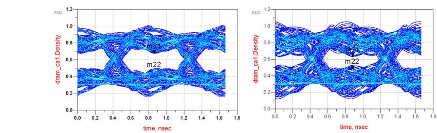
Chapter 1: Overview

PCB Design Features
       The PCB guidelines in this document cover two primary areas:

       • Power distribution:
         ○   Current step loads and device utilization

         ○   Recommended PCB decoupling capacitor quantities

         ○   Capacitor specification requirements

       • Memory interface routing:
         ○   Required routing guidelines for all memory interfaces

         ○   DDR4

         ○   LPDDR4/4x

         ○   RLDRAM3

         ○   QDR-IV

       • Schematic Design and Simulations Resources
         ○   Design Hub for PCB Board System Design
             - DDR4 and LPDDR4 Timing Models for HyperLynx DDRx Wizard in Versal ACAPs: This
               tutorial shows how to incorporate Versal DDR4 and LPDDR4 timing models into
               HyperLynx.
             - Obtaining and Verifying Versal ACAP Memory Pinouts: This tutorial offers the fast
               method for obtaining valid memory pinouts from the Vivado® tools.
             - Versal ACAP Schematic Review Checklist (XTP546): Now includes an automated
               schematic checker.
             - Xilinx Power Estimator (XPE) spreadsheet tool (download at www.xilinx.com/power):
               Includes custom decoupling requirements based on the specific design.

Differences from Previous Generations
       The Versal architecture PCB guidelines have been streamlined from prior generations to be more
       accessible to PCB layout professionals as well as hardware designers. Some examples of this
       streamlining are:

       • Assumptions used in determining PCB capacitor quantities are better explained

UG863 (v1.2) February 1, 2022                                                            www.xilinx.com
                                                                      Send Feedback
Versal ACAP PCB Design User Guide                                                                     6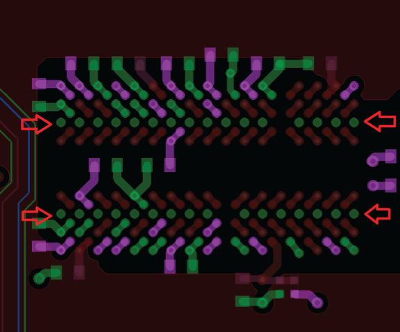
Chapter 1: Overview

       • Memory routing guidelines are geared specifically for PCB layout professionals, with easy-to-
         find guidelines and specific constraint definitions

UG863 (v1.2) February 1, 2022                                                           www.xilinx.com
                                                                     Send Feedback
Versal ACAP PCB Design User Guide                                                                    7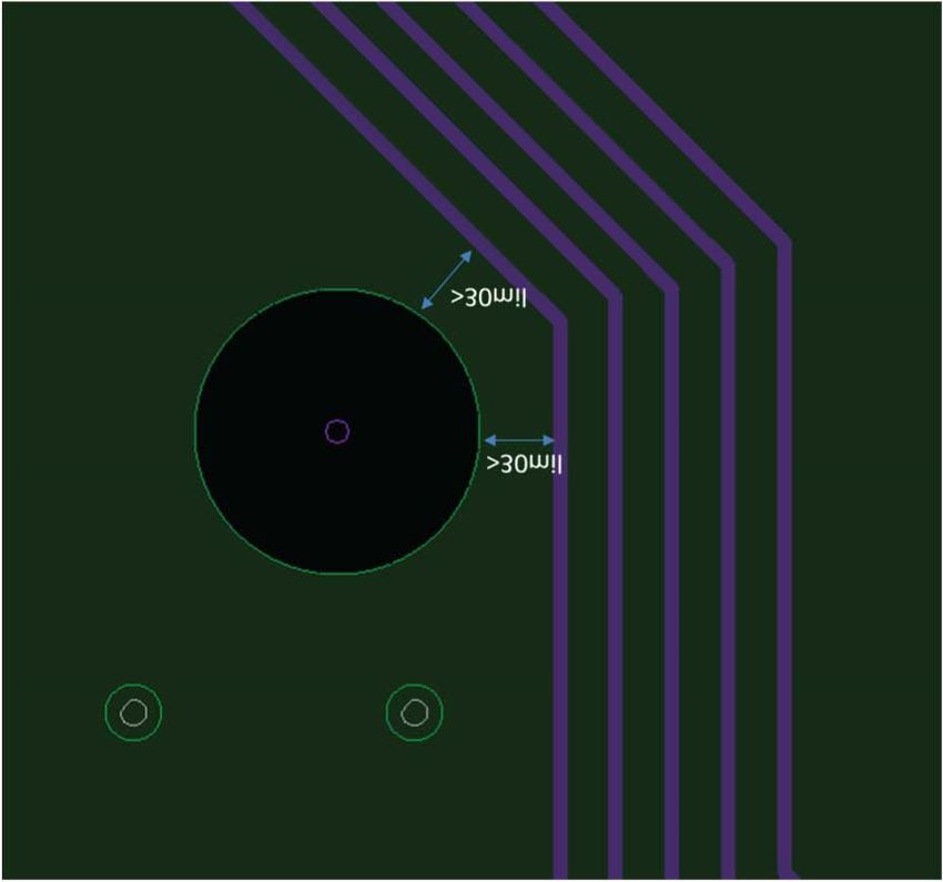
Chapter 2: Power Distribution System in Versal ACAPs

                                                                                            Chapter 2

Power Distribution System in Versal
ACAPs

Introduction
       This chapter documents the power distribution system (PDS) for Versal ACAPs, including various
       power management scenarios and obtaining decoupling quantities via the Xilinx Power Estimator
       (XPE) tool.

       For additional resources regarding board design planning, refer to the Board and Device Planning
       chapter of Versal ACAP Hardware, IP, and Platform Development Methodology Guide (UG1387).

Versal ACAP Power Rails
       Versal ACAPs contain a number of power rails that each serve a specific function, as shown in
       the following table. Refer to Versal AI Core Series Data Sheet: DC and AC Switching Characteristics
       (DS957) for the most current information regarding supply names and voltage levels.

       Table 1: Primary Versal ACAP Power Supplies

                    Power Rail                      Voltage (V)                    Circuitry Powered
       Core Rails
       VCCINT                                      0.70/0.80/0.88          Logic, AI Engine, Clocking, Block RAM/
                                                                           UltraRAM, DSP, GTY, I/O
       VCC_RAM                                       0.80/0.88             Block RAM/UltraRAM, Clocking
       VCC_SOC                                       0.80/0.88             Network-on-Chip (NOC), Memory
                                                                           Controller
       VCC_IO                                        0.80/0.88             I/O
       Auxiliary
       VCCAUX                                           1.50               AI Engine, Clocking, I/O
       Platform Management Controller (PMC)
       VCC_PMC                                     0.70/0.80/0.88          PMC

UG863 (v1.2) February 1, 2022                                                                   www.xilinx.com
                                                                        Send Feedback
Versal ACAP PCB Design User Guide                                                                            8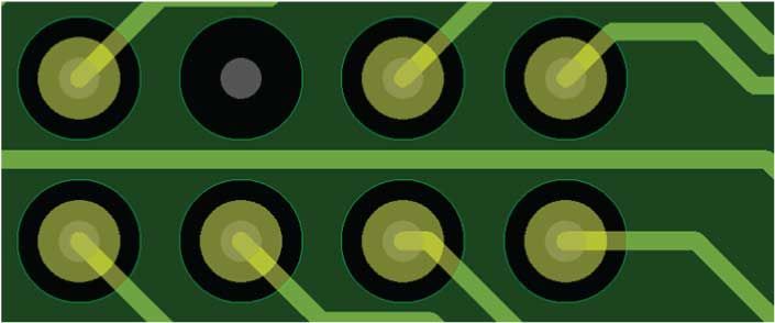
Chapter 2: Power Distribution System in Versal ACAPs

       Table 1: Primary Versal ACAP Power Supplies (cont'd)

                   Power Rail                     Voltage (V)                    Circuitry Powered
       VCCO_500, VCCO_501                          1.80 to 3.30          PMC MIO
       VCCO_503                                    1.80 to 3.30          PMC Dedicated Pins
       VCCAUX_PMC                                      1.50              PMC
       VCCAUX_SMON                                     1.50              PMC
       Processing System (PS)
       VCC_PSFP                                   0.70/0.80/0.88         PS Full Power
       VCC_PSLP                                   0.70/0.80/0.88         PS Low Power
       VCCO_502                                    1.80 to 3.30          LPD MIO
       I/O
       VCCO (multiple)                              1.0 to 3.30          XPIO, HDIO
       GTY/GTYP/GTM
       GTY_AVCC                                        0.88              GTY
       GTY_AVTT                                        1.20              GTY
       GTY_AVCCAUX                                     1.50              GTY
       GTYP_AVCC                                       0.88              GTYP
       GTYP_AVTT                                       1.20              GTYP
       GTYP_AVCCAUX                                    1.50              GTYP
       GTM_AVCC                                        0.88              GTM
       GTM_AVTT                                        1.20              GTM
       GTM_AVCCAUX                                     1.50              GTM
       VCCINT_GT                                    0.80/0.88            Digital circuits in GTM transceivers

Unused VCCO Banks
       If an XPIO bank is unused, it is recommended to tie the relevant VCCO pins to ground while
       leaving the individual I/Os unconnected, with the exceptions of banks 700 and 800 (if present).
       For banks 700, 800, 500, 501, 502, and 503, refer to the following list for rules for powering and
       not powering:

       • Banks 700 and 800 (if present) should always be powered as they enable DCI calibration for
         all of the other XPIO banks.
       • Bank 500 VCCO pins can be grounded if no MIO circuitry in that bank or system monitor
         circuitry is used.
       • Bank 501 VCCO pins can be grounded if no MIO circuitry in that bank is used.
       • Bank 502 VCCO pins can be ground if no MIO circuitry in that bank is used.
       • Bank 503 VCCO pins should ALWAYS be powered to a valid voltage because they are used in
         the boot process.

UG863 (v1.2) February 1, 2022                                                                 www.xilinx.com
                                                                      Send Feedback
Versal ACAP PCB Design User Guide                                                                          9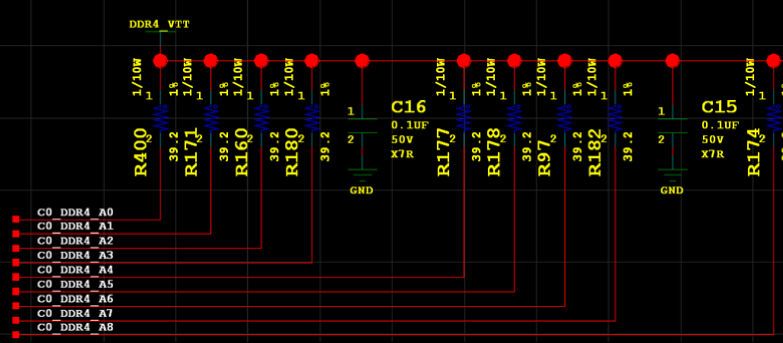
Chapter 2: Power Distribution System in Versal ACAPs

Power Management Scenarios
       While it is possible to power each rail with its own voltage regulator module (VRM), it can be
       beneficial both cost-wise and area-wise to consolidate power rails that share the same voltage.
       Xilinx has defined two power management scenarios that can be used depending on design
       needs. These power management scenarios are further defined into sub-categories depending on
       the core voltage and whether or not the processing system (PS) is powered at a higher voltage.

       • Minimum Rails: This category aims to reduce the amount of regulators and unique power rails
         on the board. This saves on complexity, component count, and board space at the expense of
         reduced flexibility in regards to powering individual rails.

       • Full Power Management: This category allows for the greatest flexibility in regards to
         powering individual rails, resulting in power savings, though with increased complexity,
         component count, and board space.

       The Xilinx Power Estimator (XPE) tool contains the full scenario descriptions with rail sequencing
       requirements, rail groupings, voltage values, voltage tolerances, and graphical images for all of the
       scenarios. XPE is intended be used along with user power estimation to ensure the most robust
       power system design.

       Note: Power delivery reference designs using these supported rail consolidations are available from Power
       Efficiency.

Recommended Decoupling Capacitor
Quantities for Versal Devices
       Recommended decoupling quantities for core, auxiliary, and VCCO rails in Versal devices can be
       obtained via the Xilinx Power Estimator (XPE) tool. XPE provides a custom set of decoupling
       guidelines based on the actual usage parameters of the design.

       The following sections illustrate the methodology that XPE uses for determining the appropriate
       number of decoupling capacitors to use for a particular power rail.

UG863 (v1.2) February 1, 2022                                                                   www.xilinx.com
                                                                           Send Feedback
Versal ACAP PCB Design User Guide                                                                            10
Chapter 2: Power Distribution System in Versal ACAPs
Decoupling Capacitor Methodology
Device Resource Utilization
The amount of decoupling required is primarily determined by the amount of power utilized by
the design. The power can be accurately estimated by using the XPE tool. By entering such usage
parameters as the number of logic cells and DSPs, an accurate current power profile can be
obtained.
Resource utilization consists (in part) of:
• AI Engine: Number of cores used, frequency, loading, and read/write rate
• Logic: Number of registers and LUTs, toggles rates, and frequency
• Block RAM: Number of block RAMs, toggles rates, enable rates, and frequencies
• URAM: Number of UltraRAMs, toggles rates, enable rates, and frequencies
• DSP: Number of DSP blocks, toggles rates, enable rates, and frequencies
• GTY: Number of GTY transceivers used, types (PCIe or MRMAC), and frequencies
• Processing System: Low Power Domain (LP): Processor speeds, loading, and interconnect
• Processing System: Full Power Domain (FP): Processor speeds, loading, and interconnect
• Processing System: I/O (MIO): Interfaces types (USB, QSPI, and eMMC) and speeds
• XPIO: I/O standards, enable rates, and frequencies
• HDIO: I/O standards, enable rates, and frequencies
Current Step Load Assumptions
The step load is the percentage of the dynamic current that is expected to be demanded at any
given switching event. This is the instantaneous current that will be provided primarily by the
decoupling capacitors until the regulators can respond. XPE has predefined step load
percentages for each rail (with VCCINT being adjustable per the specific nature of the system
design). As a point of reference, the current consumption of VCCINT has the most notable effect
on the amount of decoupling required by the system, so it is important to ensure the step load
percentage is as accurate as possible. XPE defaults to 25% step load for VCCINT, but the user
can adjust as needed based on their planned application.
UG863 (v1.2) February 1, 2022 www.xilinx.com
Send Feedback
Versal ACAP PCB Design User Guide 11Chapter 2: Power Distribution System in Versal ACAPs
Voltage Ripple Assumptions
AC voltage ripple (voltage deviation due to transient current events) along with VRM DC
tolerance on each rail is assumed to fall within the specifications as defined in the Versal ACAP
data sheets. For purposes of determining PCB decoupling, the core rails (VCCINT, VCC_RAM,
VCC_SOC, VCC_IO, VCC_PSFP, VCC_PSLP, and VCC_PMC) use a fixed 17 mV for AC ripple in
addition to a DC VRM tolerance of 1%. For example, if the Versal ACAP data sheets list a
minimum/maximum operating voltage, decoupling capacitors are designed to ensure that the AC
ripple stays within 17 mV while the rest of the margin is allocated to account for the 1% DC
tolerance of most voltage regulator modules (VRMs).
Target Impedance
Given the required ripple tolerance and step load amount, a target impedance can be calculated.
The impedance of the PDN network on the board should be targeted to be at or below this
target impedance at the typical frequency in which decoupling capacitors are most effective (see
XPE for frequency ranges). Beyond these frequencies, the internal and mounting inductances of
the capacitors reduce their effectiveness.
The formula for target impedance is shown in the following equation.
Equation 1: Target Impedance Equation
% Ripple
VoltageRailValue × 100
Z target =
StepLoadCurrent
An example calculation for a 0.80V rail specified with ±3% tolerance (1% DC, 2% AC) and 40A of
required step current is as follows:
Equation 2: Target Impedance Calculation
2
0.80 × 100
Z target = = 0.40 mΩ
40
Recall that ±2% is used as the ripple target because ±1% is assumed to be taken by the tolerance
of the VRM.
Note: For the case where the ripple tolerance is given as a fixed number such as 17 mV, use the fixed value
as the numerator in the above equation.
TIP: Xilinx recommends running a full board-level PDN simulation to confirm that the voltage
specifications are met.
UG863 (v1.2) February 1, 2022 www.xilinx.com
Send Feedback
Versal ACAP PCB Design User Guide 12Chapter 2: Power Distribution System in Versal ACAPs
Planar Resistance Recommendations
It is important to design the physical power planes in order to transfer the power required on the
rail with minimal IR voltage loss. Narrow planes, or planes with many via keep-out circles, can
lead to excessive IR drop that can be difficult to overcome by regulators, even with proper sense
line placement. Xilinx highly recommends that a proper power analysis be done to ensure that all
DC and AC specifications are followed, including simulations before and after PCB layout.
For a starting point for plane design with regard to IR drop, each power plane should be targeted
to have a voltage drop of no greater than the recommended voltage delta (typical – minimum)
when subjected to the total current expected on the rail. This voltage drop, divided by the total
current, provides the maximum amount of resistance for the rail.
RMAX = (Recommended Typical Voltage – Recommended Minimum Voltage)/Total Current
The recommended typical and minimum voltage values can be found in the datasheet, and the
total current can be found in the Xilinx Power Estimator (XPE) tool.
This maximum resistance value is solely with regard to the IR drop across the plane and does not
take into account any thermal or other requirements. The actual maximum plane resistance might
be lower when all other factors are considered.
Example 1: Planar Resistance for VCCINT
Assuming a mid-voltage device (M), the typical voltage for VCCINT is 0.80V. The corresponding
minimum voltage is 0.775V. The voltage drop is 0.80V – 0.775V = 0.025, or 25 mV. Assuming a
design that has 99A total current on VCCINT, RVCCINT = 0.025V/99A = 0.252 mΩ.
Example 2: Planar Resistance for VCCAUX
According to the datasheet, the typical VCCAUX value is 1.50V, and the minimum value is
1.455V. The voltage drop is 1.50V – 1.455V = 0.045V, or 45 mV. Assuming a design with 8A total
current, the maximum resistance is 0.045V/8A = 5.625 mΩ.
PCB Routing for Remote Voltage Sense Lines
In order to correctly compensate for IR voltage drop across the PCB due to high current loads,
proper routing of voltage regulator module (VRM) sense lines is critical for maintaining proper
voltage levels at the ACAP die.
Note: Be sure to always follow the sense line recommendations from the VRM vendors because regulator
designs, pinouts, and requirements vary.
UG863 (v1.2) February 1, 2022 www.xilinx.com
Send Feedback
Versal ACAP PCB Design User Guide 13Chapter 2: Power Distribution System in Versal ACAPs
Purpose of Sense Lines
As voltage regulators are often quite a distance away from the devices they supply power to,
there is often a DC voltage IR drop in voltage between the regulator and the main points-of-load,
especially if there is high current load. If the regulator was not accounting for this drop, the
voltage at the point-of-load can possibly be quite a bit lower than what the regulator sees. The
resulting lower voltage can thus be out of the required limits for proper device operation. The
following figure illustrates the direction of current flow and the resulting voltage drop.
Figure 1: DC Voltage Drop between VRM and Point-of-Load
ACAP
VRM
Current Flow
Voltage Drop = I R Vin
Vout VCCINT
Vout > Vin
X26050-121021
To overcome this voltage drop, regulators implement sense lines that connect directly from the
regulator to the point-of-load. These sense lines are direct traces between the regulator and
point-of-load and do not carry any current. Because they do not carry any current, the voltage at
the regulator sense pins is exactly the same as seen at the point-of-load. The regulator can thus
properly adjust its output voltage as necessary so that the voltage at the point-of-load is within
the required specification. The following figure illustrates the placement and routing of sense
lines from the VRM to the point-of-load.
UG863 (v1.2) February 1, 2022 www.xilinx.com
Send Feedback
Versal ACAP PCB Design User Guide 14Chapter 2: Power Distribution System in Versal ACAPs
Figure 2: Example of Sense Lines
ACAP
VRM
Vout VCCINT
0Ω
Vsense+
Vsense-
PCB Traces 0Ω
X26053-120921
Limitations of Sense Lines
Voltage Disparity
Because sense lines can only be placed at one location at the point-of-load, other areas in front
of the sense points might show a higher voltage, while points beyond the point-of-load might see
lower voltage. The following figure illustrates this voltage disparity. As the current flows from the
VRM to the point-of-load, the voltage at point V1 is higher than the sense point at V2. Likewise,
the voltage at point V3 is lower than at the sense point V2.
Figure 3: Voltages at Various Points in BGA Pin Field
ACAP
VRM V1 > V2 (sense point) > V3
V1 V2
Vout VCCINT
V3
0Ω
Vsense+
Vsense-
0Ω
X26054-120921
UG863 (v1.2) February 1, 2022 www.xilinx.com
Send Feedback
Versal ACAP PCB Design User Guide 15Chapter 2: Power Distribution System in Versal ACAPs
VRMs with Only One Sense Pin
Some VRMs do not include a sense pin for ground. The primary limitation of this arrangement is
that fluctuations in the ground voltage at the point-of-load are not accounted for by the VRM,
resulting in less precise voltage regulation.
ACAPs with Dedicated Sense Pins
Select Versal ACAPs contain dedicated remote voltage sense pins for VCCINT and its associated
ground return. They provide the closest look at the die possible.
The following figure shows recommended sense line routing for ACAPs with dedicated sense
pins.
• Place inline 0Ω resistors close to the ACAP:
○ Resistors are required to ensure sense lines are routed as traces and not dropped to the
plane.
• Route sense lines as 50Ω loosely coupled differential transmission lines:
○ Ground is required to sense true differential between power and ground.
Figure 4: Dedicated Sense Pin Routing
ACAP
VRM
Vout VCCINT
0Ω
Vsense+ VCCINT_SENSE
Vsense- GND_SENSE
0Ω
X26055-120921
UG863 (v1.2) February 1, 2022 www.xilinx.com
Send Feedback
Versal ACAP PCB Design User Guide 16Chapter 2: Power Distribution System in Versal ACAPs
ACAPs without Dedicated Sense Pins
For ACAPs without dedicated sense pins, the sense line connections should connect to BGA balls
that are as close as possible to the most significant point-of-load on the ACAP. This can be best
estimated via DC simulation or via the device view in the Vivado tools. If the point-of-load
cannot be estimated, placing the sense connections towards the center of the BGA pin field is
recommended. Placing at the ball furthest from the regulator is also an option, though less
preferred.
• Place inline 0Ω resistors close to the ACAP:
○ Resistors are required to ensure sense lines are routed as traces and not dropped to the
plane.
• Route sense lines as 50Ω loosely coupled differential transmission lines:
○ Ground is required to sense true differential between power and ground.
For optimum power transfer, ensure that the balls connecting to the sense lines fully connect to
their respective planes, i.e., do not leave them unconnected as “spy holes” (see the following
figure).
Figure 5: Sense Pin Routing without Dedicated Sense Pins
ACAP
VRM
Vout VCCINT
0Ω
Vsense+
Vsense-
0Ω
X26056-120921
The Use of Routing Tunnels and Sense Lines
Some Versal ACAPs have a dedicated “tunnel” of BGA pins that are specifically placed so as to
provide for the maximum amount of power delivery with minimal IR drop. This so-called routing
tunnel removes via keep-out areas that result in holes in the power plane. The pins in the routing
tunnel do not connect directly to the die on the ACAP. These pins are only present so that the
PCB routing planes for VCCINT do not require via keep-out holes from other signals or power
rails.
UG863 (v1.2) February 1, 2022 www.xilinx.com
Send Feedback
Versal ACAP PCB Design User Guide 17Chapter 2: Power Distribution System in Versal ACAPs
The following figure shows the BGA pin field of the VC1902-A2197 device with the VCCINT pin
field outlined. The pins in the routing tunnel area do not require via keep-outs to the VCCINT
planes below, so there are no holes in the metal planes that supply power to VCCINT. Optimal
sense line placement is at any point on the VCCINT pin field that is outside of the routing tunnel.
Figure 6: VC1902-A2197 with VCCINT Routing Tunnel
Routing Tunnel
X26060-120921
UG863 (v1.2) February 1, 2022 www.xilinx.com
Send Feedback
Versal ACAP PCB Design User Guide 18Chapter 2: Power Distribution System in Versal ACAPs
The following figure shows the BGA pin field of the VM1802-C1760 device with the VCCINT pin
field outlined. There is no routing tunnel on this device, so the power planes on the BGA have via
keep-outs that reduce power delivery efficiency. Sense line placements would be recommended
anywhere near the center of this pin field.
Figure 7: VM1802-C1760 VCCINT Pin Field
VCCINT
Pin Field
X26059-120921
UG863 (v1.2) February 1, 2022 www.xilinx.com
Send Feedback
Versal ACAP PCB Design User Guide 19Chapter 3: PCB Guidelines for Memory Interfaces
Chapter 3
PCB Guidelines for Memory
Interfaces
The Versal architecture provides solutions for interfacing with the following memory
architectures:
• DDR4
• LPDDR4/4x
• RLDRAM3
• QDR-IV
Before the individual architecture guidelines is a section on required guidelines that apply to all
memory interfaces.
Required Memory Routing Guidelines for All
Interfaces
The following list contains guidelines that apply to all memory interfaces (DDR4, LPDDR4/4x,
RLD3, and QDR-IV interfaces).
1. Include package delay in routing constraints when determining signal trace lengths unless
otherwise specified. When minimum and maximum values are available for the package
delay, use the midpoint/average between the minimum and maximum values.
2. DQ and DQS signals in the same byte group should be routed on the same layer from Versal
device to DRAM/DIMM. Include the data mask (DM) in the byte group as applicable.
3. Do not change layers when routing from one DIMM to the next for multi-slot topologies.
Additionally, it is recommended to route data byte groups on the highest signal layers (closest
to the DIMM connector) as much as possible. Depending on the DIMM placement, the
longest DQ bytes could be the center ones or the edge ones.
UG863 (v1.2) February 1, 2022 www.xilinx.com
Send Feedback
Versal ACAP PCB Design User Guide 20Chapter 3: PCB Guidelines for Memory Interfaces
4. For fly-by routing, address, command, and control signals can be routed on different layers,
but it is recommended to use as few as possible. Do not route any individual signal on more
than two layers to minimize inductive loops that can lead to crosstalk issues. Any signal layer
switching via needs to have one ground via within a 50 mil radius.
5. Versal device and memory drive strengths are assumed to be 40Ω. Versal device DCI and
memory ODT are assumed to be 40Ω.
6. If the system clock is connected to a bank that is also used for memory, it may be necessary
to bias the incoming clock signals so that they adhere to the signal level requirements of the
IO standard in the bank. Refer to the "AC Coupling Recommendations" section in Versal ACAP
SelectIO Resources Architecture Manual (AM010) for specific requirements. The following
figure shows the biasing structure from that document.
Figure 8: AC-Coupled with DC-Biased Differential Clock Input
1.2V
6.81 KΩ
6.81 KΩ
LVDS15 Input Buffer
RDIFF
CAC
100Ω Differential Transmission Line
CAC
2.0 KΩ
2.0 KΩ
X22485-103020
UG863 (v1.2) February 1, 2022 www.xilinx.com
Send Feedback
Versal ACAP PCB Design User Guide 21Chapter 3: PCB Guidelines for Memory Interfaces
7. Signal lines must be routed over a solid reference plane. Avoid routing over voids, as shown in
the following figure.
Figure 9: Signal Routing Over Solid Reference Plane
UG863 (v1.2) February 1, 2022 www.xilinx.com
Send Feedback
Versal ACAP PCB Design User Guide 22Chapter 3: PCB Guidelines for Memory Interfaces
8. Avoid routing over reference plane splits, as shown in the following figure.
Figure 10: Signal Routing Over Reference Plane Split
UG863 (v1.2) February 1, 2022 www.xilinx.com
Send Feedback
Versal ACAP PCB Design User Guide 23Chapter 3: PCB Guidelines for Memory Interfaces
9. Keep the routing at least 30 mils away from the reference plane and void edges with the
exception of breakout regions, as shown in the following figure.
Figure 11: Breakout Region Routing
UG863 (v1.2) February 1, 2022 www.xilinx.com
Send Feedback
Versal ACAP PCB Design User Guide 24Chapter 3: PCB Guidelines for Memory Interfaces
10. Use chevron-style routing to allow for ground stitch vias. Figure 12 shows recommended
routing for fly-by configurations, while Figure 13 shows recommended routing to
accommodate ground stitch vias in a more congested clamshell configuration.
Figure 12: Example of Ground Stitching (Fly-by)
UG863 (v1.2) February 1, 2022 www.xilinx.com
Send Feedback
Versal ACAP PCB Design User Guide 25Chapter 3: PCB Guidelines for Memory Interfaces
Figure 13: Example of Ground Stitching (Clamshell) Red: Power, Green: Ground
UG863 (v1.2) February 1, 2022 www.xilinx.com
Send Feedback
Versal ACAP PCB Design User Guide 26Chapter 3: PCB Guidelines for Memory Interfaces
The following figure shows simulated eye diagrams for a DDR4 command/address/control bit
with and without ground stitching vias. The simulation on the left shows an eye height of 180
mV with ground stitch vias, while the simulation on the right shows an eye height of only 99
mV when not utilizing ground stitch vias.
Figure 14: Simulations With and Without Ground Stitching Vias
Case 1: with GND vias Case 2: without GND vias
Eye Height (mV) 180 99
X21618-092218
11. Add ground vias as much as possible around the edges and inside the device (ACAP, memory
component, DIMM) to make a better ground return path for signals and power, especially
corners. Corner or edge balls are generally less populated as grounds.
UG863 (v1.2) February 1, 2022 www.xilinx.com
Send Feedback
Versal ACAP PCB Design User Guide 27Chapter 3: PCB Guidelines for Memory Interfaces
12. For address/command/control VTT termination, every four termination resistors should be
accompanied by one 0.1 μF capacitor, physically interleaving among resistors, as shown in
the following figure. Refer to the memory vendor’s data sheet for specifications regarding
noise limits on the address/command/control VTT lines.
Figure 15: Schematic Example of VTT Resistor and Capacitor Connections
UG863 (v1.2) February 1, 2022 www.xilinx.com
Send Feedback
Versal ACAP PCB Design User Guide 28Chapter 3: PCB Guidelines for Memory Interfaces
Figure 16: Example of VTT Termination Placement
13. For DIMM topologies, place bypass capacitors near the command/address/control pads to
provide extra ground via locations. These bypass capacitors also provide a lower impedance
path from power to ground. This is important because the address/command/control pins are
referenced to ground on the ACAP and PCB while they are referenced to power on the
DIMM.
14. For dual-slot DIMM topologies, place DIMM #0 on the furthest connector from the ACAP to
reduce the effect of SI reflections. The DIMM #1 connector should be placed nearest to the
ACAP.
15. For DDR4 interfaces with two copies of the clock and nine or more components (e.g.,
interfaces with dual-die package (DDP) devices), it is recommended to route the clocks in an
alternating pattern such that clock 1 connects to devices 1, 3, 5, 7, etc., and clock 2 connects
to devices 2, 4, 6, 8, etc. All terminations should be placed at the end of the fly-by topology.
UG863 (v1.2) February 1, 2022 www.xilinx.com
Send Feedback
Versal ACAP PCB Design User Guide 29Chapter 3: PCB Guidelines for Memory Interfaces
Figure 17: DDR4 2CK Single-Rank Configuration
2 CK pairs with DDR4 Single-Rank, x16 DDP (x8 per die) Component Interface
X8 X8
ACAP DRAM #1 DRAM #2 DRAM #3 DRAM #4 DRAM #5
CK0_T/C
CK1_T/C
TERM TERM
X25088-021721
Figure 18: DDR4 2CK Dual-Rank Configuration
2 CK pairs with DDR4 Dual-Rank, x8 DDP (x8 per die) Component Interface
X8, X8,
Rank0 Rank1
DRAM DRAM DRAM DRAM DRAM DRAM DRAM DRAM DRAM
ACAP #1 #2 #3 #4 #5 #6 #7 #8 #9
CK0_T/C
CK1_T/C
TERM TERM
X25089-021721
UG863 (v1.2) February 1, 2022 www.xilinx.com
Send Feedback
Versal ACAP PCB Design User Guide 30Chapter 3: PCB Guidelines for Memory Interfaces
16. For clamshell configurations that use address mirroring, ensure that both chip select lines
have adequate decoupling at their terminations as well as sufficient plane/trace thicknesses
to/from VTT.
Reference Material Specifications
The guidelines in this chapter were determined based on the following PCB material
specifications. Signal integrity simulations are encouraged for any material or specifications that
deviate from those listed here.
• Board material: Megtron 6 class
• Dielectric constant: ~3.7
• Dissipation factor: 0.002
• Board thickness: 65 mil
• Layer Order: Ground-signal-ground
Adjusting for Different Stack-Ups
The trace width, spacing, length, and skew constraints presented in this chapter are based on the
reference PCB materials listed in Reference Material Specifications. When not using these
specific parameters, trace width, lengths, layer heights, spacings, and dielectric material could
need adjustments to meet the impedance, length, and skew specifications.
The PCB fabrication house can adjust these factors to achieve the desired impedance and
propagation delay targets. The effects of each of these items are listed in this section. In addition,
a two-dimensional field solver utility allows for various combinations to be tested.
Dielectric Material
Each dielectric material has its own relative dielectric constant (DK) and dissipation factor/loss
tangent (DF) that are contributing factors to line impedance (Z0), signal propagation delay (TPD),
and signal loss (α). As DK increases, impedance decreases while the signal propagation delay and
signal loss increase, and vice versa. A typical DK found on PCBs ranges from 3.4 to 4.6. The
propagation delay in a given dielectric material is constant and is not affected by any other board
parameters such as layer height, conductor width, or conductor spacing. Propagation delay is
affected by frequency, but the effect is minimal with regards to typical memory speeds. Signal
loss is also affected by frequency, with the loss increasing with increasing frequency.
The following equation shows the calculation for propagation delay (TPD), with DK as the
dielectric constant, and c as the speed of light in free space (2.998 x 10⁸ m/s or 1.180 x 10¹⁰
in/s).
UG863 (v1.2) February 1, 2022 www.xilinx.com
Send Feedback
Versal ACAP PCB Design User Guide 31Chapter 3: PCB Guidelines for Memory Interfaces
Equation 3: Propagation Delay Calculation
√ DK
T PD = c
The associations in the following table show the effect of the dielectric constant (DK) on the
impedance (Z0), propagation delay (TPD), and signal loss (α).
DK ↑ Z0 ↓ TPD ↑ α↑
DK ↓ Z0 ↑ TPD ↓ α↓
Trace Width
As the trace width (W) increases, the impedance decreases while the signal propagation delay
remains unchanged, and vice versa. Any adjustments in width should include adjustments in
spacing (S) to maintain immunity to crosstalk effects. Spacing factors are roughly 1.0X to 3X
depending on the particular type of memory and signal. The associations in the following table
show the effect of width on impedance, spacing, and propagation delay.
W↑ Z0 ↓ S↑ TPD (no change)
W↓ Z0 ↑ S↓ TPD (no change)
Layer Height
As the layer height (H) is increased, the impedance increases while the signal propagation delay
remains unchanged, and vice versa. When reducing or increasing layer height, consider that layer
heights that are too low can be more expensive to reliably manufacture because the PCB
fabricator must avoid plane shorts. Layer heights that are too high can lead to aspect ratio
violations. The associations in the following table show the effect of layer height on impedance
and propagation delay.
H↑ Z0 ↑ TPD (no change)
H↓ Z0 ↓ TPD (no change)
Base Copper Weight
As the base copper weight (Cu oz) of the conducting lines is increased, the impedance decreases
while the signal propagation delay remains unchanged, and vice versa. The most common base
copper weight used in PCBs is 0.5, known as half-ounce copper. The effect of changing the base
copper weight is minimal, however, and is not recommended due to the potential for increased
costs in relation to the small benefit typically gained.
UG863 (v1.2) February 1, 2022 www.xilinx.com
Send Feedback
Versal ACAP PCB Design User Guide 32Chapter 3: PCB Guidelines for Memory Interfaces
Example of Tuning Design Parameters to Meet Impedance Targets
The following table shows a target of 45Ω for stripline impedance in the main L1 PCB area. The
trace width (W) is specified as 7.0 mils, DK of 3.71, and height of 6.7 mils. The table also shows
tuning of the dielectric constant, trace width (W), and height (H) required to meet the impedance
target. The spacing (S) shows how it should change in order to continue to meet performance
requirements, though the spacing is not a factor in the line impedance. When increasing DK, the
signal loss also increases as shown in the table.
Table 5: Example of Tuning PCB Parameters to Meet Impedance Target
Target
Material DK W (mil) S (mil) H (mil) Change from Reference
([Z0] Ω)
45 Megtron 6 3.71 7.0 - 6.7 Reference
45 Megtron 6 3.71 7.5 ↑ ↑ 7.15 ↑ Same DK, bigger width, taller
height
45 Megtron 6 3.4 ↓ 7.0 - 6.27 ↓ Lower DK, same width, lower
height
45 Megtron 6 3.4 ↓ 7.5 ↑ ↑ 6.7 Lower DK, bigger width,
same height
PCB Routing Guidelines for DDR4 Interfaces
This section provides PCB design guidelines for DDR4 interfaces. Connections between the
ACAP and DDR4 device(s) are defined along with physical design rules and timing constraints.
Both component and DIMM architectures are covered.
IMPORTANT! All routing guidelines in this section must be followed to achieve the maximum data rates
specified in the Versal ACAP data sheets. Customers could have unique or specific designs with particular
violations of some rules. In these scenarios, design or routing trade-offs have to be taken in other routing
parameters to mitigate the risk. System-level channel signal integrity simulations are required to evaluate
such trade-offs. It is important to read Required Memory Routing Guidelines for All Interfaces before
continuing with this section.
Signals and Connections for DDR4 Interfaces
The required signals used in DDR4 applications are shown in the following table. The signal list
might vary slightly depending on the particular DDR4 architecture used.
IMPORTANT! For dual-slot DIMM topologies, place DIMM #0 on the furthest connector from the ACAP
to reduce the effect of SI reflections. The DIMM #1 connector should be placed nearest to the ACAP.
UG863 (v1.2) February 1, 2022 www.xilinx.com
Send Feedback
Versal ACAP PCB Design User Guide 33Chapter 3: PCB Guidelines for Memory Interfaces
Table 6: DDR4 Signal Definitions
Required PCB Signal Routing
Signal Description
Termination1 Methodology
Clock Signals
CK_T/CK_C2 Address/Command Clock See Figure 20 Fly-by
Address Signals
A[17], A[13:0] Address 39Ω to VTT at far end Fly-by
RAS_N/A[16] Row Access Strobe 39Ω to VTT at far end Fly-by
CAS_N/A[15] Column Access Strobe 39Ω to VTT at far end Fly-by
WE_N/A[14] Write Enable 39Ω to VTT at far end Fly-by
BA[1:0] Bank Address 39Ω to VTT at far end Fly-by
BG[1:0] Bank Group 39Ω to VTT at far end Fly-by
Command/Control Signals
ACT_N Activate Command 39Ω to VTT at far end Fly-by
CKE Clock Enable 39Ω to VTT at far end Fly-by
CS_N Chip Select 39Ω to VTT at far end Fly-by
ODT On-Die Termination Enable 39Ω to VTT at far end Fly-by
PAR Command/Address Parity 39Ω to VTT at far end Fly-by
Data Signals
DQ byte/nibble Data None, uses ODT Point-to-point
(8 or 4 bits each)
DM/DBI Data Mask/Data Bus None, uses ODT Point-to-point
(If present, one per byte) Inversion
Data Strobe Signals
DQS_T/DQS_C Data Strobe None, uses ODT Point-to-point
(one pair per byte/nibble)
Miscellaneous Signals
RESET_N Reset 4.7 kΩ to GND at far end Fly-by
DDR4 Devices/DIMMs Only
ALERT_N (devices) CRC Error Flag Open-Drain Tie all ALERT_N pins in same Shared Pull-up
Output interface to DRAM VDD
through 50Ω resistor if not
used in system
TEN (devices) Connectivity Test Mode Input 500Ω to GND One per memory device
ZQ (devices) Calibration Reference 240Ω to GND One per memory device
EVENT_N (DIMM) Temperature Event Open- Tie all EVENT_N pins in same Shared Pull-up
Drain Output interface to VDDSPD through
4.7 kΩ resistor
UG863 (v1.2) February 1, 2022 www.xilinx.com
Send Feedback
Versal ACAP PCB Design User Guide 34Chapter 3: PCB Guidelines for Memory Interfaces
Table 6: DDR4 Signal Definitions (cont'd)
Required PCB Signal Routing
Signal Description
Termination1 Methodology
ACAP Device Only
IO_VR_700 Calibration Reference 240Ω to VCCO_700
IO_VR_800 (if present) 240Ω to VCCO_800 (if
present)
Notes:
1. Clock and address/command/control signals only require PCB termination for component interfaces.
2. To reduce loading on CK when using DDP-wide or DDP-deep component interfaces, two CK pairs are required for
interfaces that have larger than nine loads and a data rate of 1866 Mb/s or higher.
3. For more information, see Figure 17 and Figure 18.
UG863 (v1.2) February 1, 2022 www.xilinx.com
Send Feedback
Versal ACAP PCB Design User Guide 35Chapter 3: PCB Guidelines for Memory Interfaces
IMPORTANT! For single-rank and single-slot RDIMM configurations using the Optimum setting for Future
Expansion for PCB Design in the Vivado AXI NoC IP customization tool, the DDR4 output clock pin sites
are swapped in the nibble. The CK_T pin is at an N site and the CK_C pin is at a P site. This is a known
behavior and does not have any functional impact during operation. Do not manually swap these pins on
the external memory interface because this will cause the DDR4 clock to be out of phase with the rest of
the external signals.
Command/address/control (CAC) signals are routed in a fly-by pattern with far-end termination.
DQ and DQS signals are routed point-to-point. The following figure shows examples of fly-by
and point-to-point routing.
Figure 19: Point-to-Point (DQ/DQS) and Fly-by (CAC) Routing
Point-to-Point Fly-by
DRAM
DRAM
ACAP ACAP DRAM
DRAM
DRAM
DRAM
DRAM
DRAM
X21600-051320
IMPORTANT! When creating a DDR4 interface, all components in the interface must be the same (i.e.,
share the same part number, data width, density, and speed grade).
Figure 20: Far-End Termination for Differential Clock CK_T/CK_C (Component
Interfaces Only)
VCCO/1.2V
0.01 µF
36Ω 36Ω
CK_T
CK_C
X21601-062120
UG863 (v1.2) February 1, 2022 www.xilinx.com
Send Feedback
Versal ACAP PCB Design User Guide 36Chapter 3: PCB Guidelines for Memory Interfaces
Physical Design Rules for DDR4 Signals
The following table defines routing rules for DDR4 signals.
Table 7: Physical Design Rules for DDR4 Signals
Parameter Value
Impedance Rules
Impedance for single-ended CAC1 and data signals 50Ω2 ± 10%
Impedance for differential clock (CK) and data strobe (DQS) 90Ω2 ± 10%
Trace Length Rules (from ACAP to Furthest Device or Termination)
Maximum PCB trace length for CAC signals 11000 mils
Maximum PCB trace length for data/strobe signals 5500 mil
Spacing Rules for CAC Signals
Minimum spacing between CAC signals 2H3, except:
1H under ACAP
1.5H under DDR4 device
Minimum spacing between CAC signals and clock signals 5H, except:
2H under ACAP
2H under DDR4 device
Minimum spacing between CAC signals and data signals 5H, except:
2H under ACAP
2H under DDR4 device
Spacing Rules for Data and Data Strobe Signals
Minimum spacing between data/strobe signals within the same byte 2H, except:
1H under ACAP
1.5H under DDR4 device
Minimum spacing between data/strobe signals to data/strobe signals in other 5H, except:
bytes 2H under ACAP
2H under DDR4 device
Spacing Rules for Signals between Memory Interfaces
Minimum spacing between signals in one memory interface to signals in another 5H, except:
memory interface 2H under ACAP
2H under DDR4 device
Maximum Via Count per Signal Type
CAC signals and clock signals (2 × # of devices) + 2
Data and strobe signals 2
Other Physical Design Requirements
Do not route CAC/clock signals on more than two internal signal layers
Do not route data/strobe signals on more than one internal signal layer
UG863 (v1.2) February 1, 2022 www.xilinx.com
Send Feedback
Versal ACAP PCB Design User Guide 37Chapter 3: PCB Guidelines for Memory Interfaces
Table 7: Physical Design Rules for DDR4 Signals (cont'd)
Parameter Value
Route data/strobe signals on internal layers as close to the memory devices as possible
Notes:
1. CAC stands for command/address/control.
2. Up to 60Ω (single-ended) or 120Ω (differential) under ACAP or DRAM devices, taking into account PCB manufacturing
tolerances.
3. H is the distance to the nearest ground return plane.
Routing Rule Changes for Thicker Printed Circuit
Boards
The DDR4 routing rules provided in this chapter allow for the interface to run at the maximum
supported data rates as specified in the Versal ACAP data sheets while also assuming a maximum
board thickness of 131 mils. For boards thicker than 131 mils, the maximum interface speed
might need to be adjusted downward. See the following table for maximum memory data rates
per board thickness.
Table 8: DDR4 Maximum Data Rates per Board Thickness
Component Board Thickness (mil)
DDR4 ≤100 101–145 101–145 + Stub-free1 145–275
Component See Versal ACAP data Two memory speed See Versal ACAP data Three memory speed
sheets grades lower from sheets grades lower from
data rates in Versal data rates in Versal
ACAP data sheets ACAP data sheets
1-Rank DIMM See Versal ACAP data See Versal ACAP data See Versal ACAP data One memory speed
sheets sheets sheets grades lower from
data rates in Versal
ACAP data sheets
2-Rank DIMM See Versal ACAP data See Versal ACAP data See Versal ACAP data One memory speed
sheets sheets sheets grades lower from
data rates in Versal
ACAP data sheets
4-Rank DIMM See Versal ACAP data See Versal ACAP data See Versal ACAP data One memory speed
sheets sheets sheets grades lower from
data rates in Versal
ACAP data sheets
Notes:
1. Stub-free refers to alternating the routing of the signals between upper and lower layers such that long via stubs are
avoided. See Figure 22 as an example of alternate layer routing as compared to conventional routing shown in Figure
21.
UG863 (v1.2) February 1, 2022 www.xilinx.com
Send Feedback
Versal ACAP PCB Design User Guide 38Chapter 3: PCB Guidelines for Memory Interfaces
Figure 21: Conventional Routing
DRAM 1 DRAM 2 DRAM 3 DRAM 4
VTT
ACAP
Via RTT
L1 L2 L3 L4 L5
PKG
DRAM
Via
ACAP
Long Stubs
X26033-112221
Figure 22: Stub-Free Routing
DRAM 1 DRAM 2 DRAM 3 DRAM 4
VTT
ACAP L2 L4
Via RTT
L1 L3 L5
PKG
DRAM
Via
ACAP
X26034-112221
Timing Constraint Rules for DDR4 Signals
The timing constraints are defined in the following tables for various signal groups and their
targets, similar to how they would be entered into PCB layout software tools. ACAP package
delays should always be included for purposes of determining skews.
UG863 (v1.2) February 1, 2022 www.xilinx.com
Send Feedback
Versal ACAP PCB Design User Guide 39You can also read