Digital Storage and Memory Technology (Part 1) - Tom Coughlin, Roger Hoyt, and Jim Handy - IEEE ...
←
→
Page content transcription
If your browser does not render page correctly, please read the page content below
Digital Storage and Memory
Technology (Part 1)
Tom Coughlin, Roger Hoyt, and Jim Handy
November 2017

This work is licensed under a Creative Commons Attribution-NonCommercial 3.0 United States License.
This report is the first of a two-part series for the IEEE discussing developments in
 digital storage technology. In this first part, the opening section looks at developments
 in basic digital storage and memory technology at the storage and memory device
 level, extending to interfaces and protocols for connecting storage systems such as
 hard disk drives (HDDs) and solid-state drives (SDDs) to other computer hardware to
 create storage systems.

 The second section discusses developments in storage systems and software to
 manage that storage. Developments and expected developments in semiconductor
 memories are examined as well as the move from volatile to nonvolatile memory,
 including flash memory and emerging nonvolatile memories such as three-
 dimensional (3-D) XPoint and magnetic random-access memory (MRAM). Current
 and expected developments in HDD and magnetic tape technology as well as optical
 storage technology are reviewed. Important factors that prompt storage-system
 developers to use one or more of these storage technologies to create working
 storage systems are described.

 The final section looks at the business of storage and memory, comparing capital
 equipment costs, industry consolidation trends, regional developments, and
 employment, ending with recommendations for industry professionals to remain
 relevant and employed during this time of intense change in the memory and storage
 industry.

2

Table of Contents

 Table of Contents ......................................................................................................... 3
 Storage and Memory Device Developments...................................................................... 5
 Hard-Disk Drives .................................................................................................................. 6
 Magnetic Tape ...................................................................................................................... 8
 Optical Storage ..................................................................................................................... 9
 Flash Memory ..................................................................................................................... 10
 Emerging Nonvolatile Memory Technologies .......................................................................... 12
 Choosing Storage Technologies...................................................................................... 13
 Response time ............................................................................................................................ 14
 Touch rate ................................................................................................................................... 15
 Touch rate versus response time ............................................................................................ 15
 Technology regions .................................................................................................................... 16
 I/O object size curve .................................................................................................................. 17

 Digital Storage Interfaces, Protocols, and Form Factors ................................................... 20
 Device Interfaces: SATA, SAS, NVMe, and the Memory Channel ................................ 20
 SATA ............................................................................................................................................ 20
 SAS............................................................................................................................................... 22
 NVMe over PCIe......................................................................................................................... 22
 Memory Channel ........................................................................................................................ 23
 Network Interfaces: Ethernet, Infiniband, and NVMe-oF ............................................... 25
 Ethernet ....................................................................................................................................... 25
 InfiniBand ..................................................................................................................................... 26
 NVMe over fabric ........................................................................................................................ 26

 Business Trends for Storage and Memory Devices........................................................... 27
 Capital Investments, Regional Developments, and Industry Consolidation .............. 27
 Recommendations for Industry Professionals............................................................... 28
 How IEEE Can Help You Stay Employable...................................................................... 29

 Biographies .................................................................................................................... 31

3
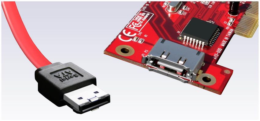
Table of Figures
 Figure 1. Data created compared to data stored. (Reproduced by Tom Coughlin from the
 Seagate Technology keynote talk at the 2017 Flash Memory Summit.) ............................. 5

 Figure 2. The ASTC HDD areal density road map. (Courtesy of ASTC.).................................... 7

 Figure 3. The LTO magnetic tape road map. (Courtesy of the LTO Consortium.) ................... 9

 Figure 4. The Blu-ray optical disc road map. ................................................................................ 10

 Figure 5. The NAND flash technology road map. (Courtesy of TechInsights.) ....................... 11

 Figure 6. A smart modular nvNITRO NVMe storage device. (Courtesy of Everspin.) ............ 12

 Figure 7. Memory-storage hierarchy versus performance. (Objective Analysis, 2017.). ....... 14

 Figure 8 The touch rate versus response time, indicating various types of uses. ................... 16

 Figure 9. The storage technology regions overlaid on the touch rate/response time chart in
 Figure 8. ....................................................................................................................................... 17

 Figure 10. The touch per year and response time for 100% random I/O in a 4-TB capacity
 HDD. ............................................................................................................................................. 18

 Figure 11. Touch per year and response time for 4-TB capacity HDD, LTO tape, and Blu-ray
 discs. ............................................................................................................................................ 19

 Figure 12. History and projections for annual shipped capacity of magnetic tape, SSDs (with
 NAND flash), and HDDs. (Coughlin Associates, 2017.)....................................................... 20

 Figure 13. SATA cable and connector. (Courtesy of SATA-IO.). .............................................. 21

 Figure 14. An M.2 form factor NVMe storage device. (Courtesy of Samsung.). ..................... 23

 Figure 15. An NVDIMM-N block diagram. (Objective Analysis, 2017.). .................................... 24

 Figure 16. A Samsung flash factory in Xi’an, China. (Courtesy of Samsung.) ........................ 28

4
Storage and Memory Device Developments

 International Data Corporation has estimated that, in 2016, 16 zettabytes (ZB, 10 to
 the 21st power bytes) of data were created and that this amount of generated data will
 increase to 163 ZB by 2023. At the same time, the shipped storage capacity for HDDs,
 magnetic tape, and flash memory was about 4.3% of the estimated generated ZB in
 2016 (0.7 ZB) and is expected to be between 2 and 3% of the estimated total ZB
 generated in 2023. This is because most of the data generated are meant to be
 processed and used, rather than stored as raw data. For instance, sensor data from
 the Internet of Things (IoT) devices or driving assistance in cars are meant to be
 processed to make real-time decisions and require memory and storage to enable this
 processing. The results of this processing might be stored for a longer time. Figure 1
 shows a visual representation of estimated data generated and stored out to 2025.

 Figure 1. Data created compared to data stored. (Reproduced by Tom Coughlin
 from the Seagate Technology keynote talk at the 2017 Flash Memory Summit.)

 Thus, different types of nonvolatile memory and digital storage are required for
 different applications. Further, more than one technology might be used together with
 others to achieve the optimal tradeoff in cost versus performance. This results in a
 hierarchy of memory and storage technologies.

 Digital storage and memory technologies began in the 1950s with the introduction of
 digital magnetic tape, magnetic HDDs, magnetic drums, and various early memory
 technologies. Since their introduction, digital storage and nonvolatile memory have
 broadened to encompass a wide range of technologies and applications. Current
 technologies include solid-state nonvolatile flash memory based on NAND
 semiconductor cells, ferroelectric, MRAM, magnetic recording on rigid disks and tape,
 and a number of different optical storage technologies.

5
The list of potential additional emerging digital storage and nonvolatile memory
 technologies that have already or may soon enter the mainstream continues to
 increase, including solid-state phase-change memory (PCM) such as Intel’s Optane,
 hybrid flash/disk drives, various resistive memory storage, spin-torque MRAM, and
 other magnetic spin-based memories and optical holographic-based storage.

 Hard-Disk Drives
 Magnetic-recording-based HDD technology continues to play a large and important
 role in mass data storage. With about 424 million shipped units in 2016 and expected
 volumes slowing to ~317 million units by 2022, HDD technology continues as a cost-
 effective, nonvolatile online storage solution (particularly for cooler long-term data
 storage). Price reductions and cost efficiencies led to vertical integration of all but one
 of the remaining three HDD manufacturers (Western Digital, Seagate Technology, and
 Toshiba) and the further consolidation of head, disk, electronics, and mechanical
 suppliers.

 Enablers for continued HDD areal density and performance improvements include
 current perpendicular-to-plane giant magnetoresistance (CPP GMR) heads, heat-
 assisted magnetic recording, microwave-assisted magnetic recording, shingled
 magnetic writing, bit patterned media, advanced signal processing, and improved
 security through disk data encryption.

 HDDs are gradually declining in the personal computer market although, for users who
 need 1-TB or higher capacity, they are still the preferred storage media because of
 their lower cost. These HDDs may be combined with an SSD or act as a hybrid HDD
 with embedded flash memory to improve the overall drive performance. The main
 growth in HDDs will be for inexpensive storage for content repositories that need lower
 latencies than magnetic tape and optical library systems (note that HDD costs are now
 lower than US$.04 per raw gigabyte). While total unit shipments are expected to
 decline going forward, the consolidation in the industry and the growing importance of
 enterprise HDD storage will limit the decline in total HDD revenue (and profit).

 The Advanced Storage Technology Consortium (ASTC), consisting of representatives
 from HDD companies as well as major HDD component vendors, creates annual road
 maps for HDD technology. In particular, the ASTC charts the areal density of magnetic
 recording over time. The areal density is the number of bits that can be stored on a
 unit of disk surface and the product of the average track density on a disk surface
 times the average linear density around those tracks. Figure 2 shows the 2016 ASTC
 HDD technology road map.

 Perpendicular magnetic recording (PMR) was introduced into HDDs in 2004. At that
 time, HDD areal density growth was over 100% annually (so you could buy over twice
 the storage capacity for the same sized disk drive from one year to the next). Today,
 nearing the end of the density improvements possible with perpendicular recording
 alone, annual areal density growth is between 10 and 15%. HDD areal densities will
 need to continue growing to retain their cost advantage over other storage
 technologies.

6
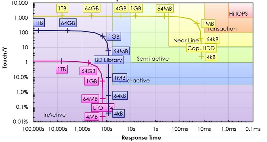
Figure 2. The ASTC HDD areal density road map. (Courtesy of ASTC.)

 To continue areal density growth, new technologies must be used in HDDs. Shingled
 magnetic recording writes adjacent tracks overlapping one another (like shingles on a
 roof) to increase the track density, while two-dimensional magnetic recording
 combines this with multiple read heads on adjacent tracks. These technologies can
 increase the areal density, but they are best used for HDDs that write data only once
 because overwriting previous data involves a multistep process that increases the
 write time of the drive. For applications that need to rewrite often, other approaches to
 increase areal density must be used.

 Up until October 2017, this additional improvement was expected to be what is called
 heat-assisted magnetic recording (HAMR), where a laser is used to allow the HDD
 write transducer to write on very-high-coercivity magnetic recording media on a disk
 surface. The high coercivity allows writing higher linear densities, but conventional
 write heads can’t produce sufficient field to write this media. The heat of the laser
 lowers the media coercivity, so the write head can write on the media. HAMR is the
 approach that Seagate Technology has announced it will use for the next generation
 of HDDs, with engineering samples available in 2018 and products in 2019.

 In October 2017, HGST, a division of Western Digital, announced it would manufacture
 HDDs that used another technology to help write heads write on high-coercivity media.
 HGST plans to put a spin-torque oscillator into the gap of the write head that will
 generate microwaves of high enough energy to help the write head write on the media.
 This approach is called microwave-assisted magnetic recording (MAMR). Western
 Digital says that engineering samples of these products will be available in 2018, with

7

production in 2019. The company also says that MAMR will allow it to increase areal
 density by 15% annually, making 40-TB HDDs possible by 2025.

 Whether using HAMR or MAMR, higher-capacity direct-overwrite HDDs will be
 available with higher storage capacities into the next decade. These HDDs will enable
 storing the vast bulk of the world’s data with acceptable latency and data rate at a low
 price.

 Magnetic Tape
 Linear tape technology leverages as much as possible from the much higher-volume
 and more advanced disk drive industry. Tape-drive developers use a number of
 technologies available from disk drives. These include read and write heads, read
 preamplifiers, write driver electronics, channel electronics such as partial-response
 maximum-likelihood (PRML) coding and detection, servo control systems, and error-
 correction codes.

 The challenge for the tape-drive developer is to adapt these technologies to
 multichannel devices. With multiple channels recording or reading simultaneously, the
 error correction code can be spread across all of the channels and thus provide added
 reliability in recovering the data. It is noteworthy that, although tape has dependencies
 on technology developed earlier for disk drives, tape products currently deliver one to
 two orders of magnitude higher bit-error reliability than disk products.

 Linear tape-open (LTO) tape cartridges (the most popular digital tape format) include
 a built-in file system capability. This file system, called the linear tape file system
 (LTFS), was first introduced with the LTO-5 tape format and expands the capabilities
 of tape library systems. The LTFS allows network-attached storage (NAS)-like single-
 tape behavior and, in library systems, also allows faster access time to data. Recently,
 RESTful application programming interfaces using LTFS tapes have also enabled
 object-based storage built around the use of magnetic tapes. The LTO road map was
 recently extended two more generations to LTO-12; see Figure 3.

8

Figure 3. The LTO magnetic tape road map. (Courtesy of the LTO Consortium.)

 LTO tapes are now available with a price below US$.01 per gigabyte of storage
 capacity. The latest LTO-8 tapes offer 12 TB of native (uncompressed) storage
 capacity and over 470 MB/s sustained data rates.

 LTO-12 will support 192 TB of uncompressed storage capacity. With new LTO
 generations being introduced roughly every three years, LTO-12 should be available
 by 2029. Recent laboratory demonstrations by IBM and Sony have shown magnetic
 tape areal densities on sputtered film tape of 201 Gb/i2, which would lead to a 330-TB
 uncompressed LTO-style cartridge.

 Optical Storage
 Digital optical discs have been used to record and store information since the 1980s.
 Optical discs record information by creating areas of differing contrast on the disc
 surface that are used for encoding digital bits. While the bulk of optical discs have
 been used for the distribution of music and video, there has long been a market for
 consumer and enterprise write-once and write-multiple-time products. While optical
 drives are becoming scarce in computers, they are still being used for write-once
 archiving of content by some organizations. The latest generation of optical media
 employed for data archiving uses Blu-ray technology. Figure 4 shows a road map for
 write-once Blu-ray optical storage technology for archiving applications released by
 Sony and Panasonic.

9

Figure 4. The Blu-ray optical disc road map.

 Blu-ray write-once optical discs are now available with 300 GB per disc capacity.
 These discs are combined into cartridges containing 12 discs (resulting in a 3.3-TB
 total cartridge capacity) that are loaded in a library system, like the tape libraries used
 by many organizations. By 2018 or 2019, it is expected that 500-GB discs will be
 available, with 1-TB discs expected by 2021–2022 (based upon Blu-ray Archive Disc
 statements). Like magnetic tape, optical discs are used for high-latency archive
 applications.

 Flash Memory
 As the fastest-growing market in the history of semiconductors, NAND flash has
 expanded to over US$35 billion in annual revenues, largely by displacing other storage
 media and enabling new applications.

 This significant growth was fueled by NAND’s cannibalization of the film market for
 cameras, the videotape market in camcorders, the floppy disk market with universal
 serial bus (USB) flash drives, and the compact disc (CD) market in MP3 players and
 digital maps, as well as the use of CD-R and CD-RW for data sharing. The technology
 also grew by displacing small form factor hard drives in MP3 players and camcorders
 and some HDDs in laptop computers, and it is gradually replacing high-performance
 HDDs used in enterprise and data-center applications.

 Although NAND flash solid-state drives have replaced HDDs in several markets, they
 have also served to complement HDDs as a nonvolatile cache between HDD storage
 and dynamic RAM (DRAM) main memory. Spending an equivalent amount of money
 on flash memory capacity generally provides a greater performance improvement than
 spending that money on more DRAM. Thus, NAND flash represents a threat to DRAM
 memory growth.

10
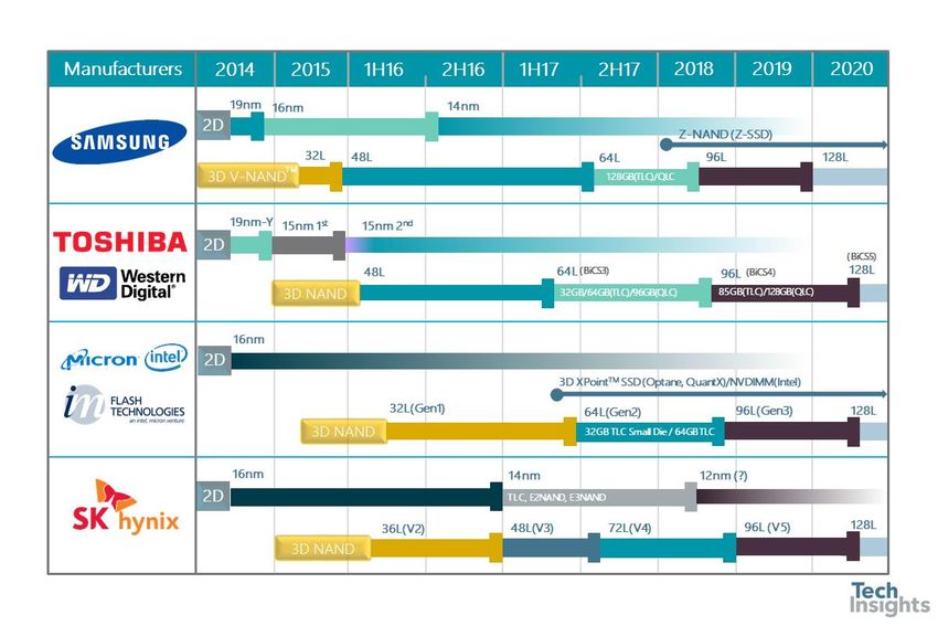
Flash memory-based SSDs are poised to become the primary storage for many
 enterprise applications, with HDDs being used for higher-latency, cooler storage.
 Although, due to greater manufacturing costs but lower storage capacity, flash
 memory is more expensive than HDD technology on a raw cost per terabyte basis,
 there are some applications where flash memory is approaching or has achieved
 operating cost parity with HDDs.

 It is anticipated that flash memory will continue to play a larger role in both low- and
 high-end computing systems as well as consumer products, as prices decline and
 capacity and reliability improvements are realized. The price decline may be faster
 than that expected based on Moore’s law, enabled by capacity improvements from
 multibit cells and three-dimensional (3-D) multilayer flash memory, although scaling
 limits due to small cell size and fundamental signal-to-noise limits may eventually
 inhibit the technology’s advance. Also, the endurance tradeoffs for increasing the
 number of bits per cell may not be acceptable for high write applications. Current flash
 memory products are up to 4 b per cell and 64 3-D layer stacks. In 2017, Western
 Digital (SanDisk), Toshiba, and Samsung announced that they would start to
 manufacture 92- to 96-layer 3-D NAND products.

 As
 Figure 5 shows, products with 128 layers and higher should become available by the
 end of the decade, likely with up to 4 b per cell. Laboratory demonstrations show that
 several-hundred-layer 3-D flash memory may be possible.

 Figure 5. The NAND flash technology road map. (Courtesy of TechInsights.)

 Flash memory is temporarily in short supply compared to demand (and thus higher
 cost) as the industry transitions to 3-D structures to continue the increase in storage
 capacity per chip, because planar flash memory line widths have nearly reached their

11
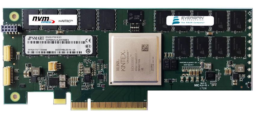
minimum. While prices for flash memory at the end of 2017 were higher than a year
 ago, these should start to decrease again in 2018 as the 3-D fabricators become fully
 online.

 Emerging Nonvolatile Memory Technologies
 New solid-state storage technologies will displace today’s prevailing technologies only
 by offering better value in the markets they serve. All technologies have technical
 weaknesses that position them for replacement. For example, HDDs drain battery life;
 and, although NAND flash memory may offer nonvolatility, it suffers from slow writing
 speeds and a limited number of rewrite cycles. However, these emerging memories
 have found niche applications and are likely to find ways to displace other memory
 technologies or enable new applications.

 Today’s most promising alternative technologies are MRAM, viewed as a potential
 successor to DRAM; resistive RAM (ReRAM), which many expect to inherit the market
 for NAND flash; and PCM, which is being newly promoted in the role of an additional
 memory/storage layer to fit between NAND flash and DRAM.

 MRAM is a nonvolatile memory based on magnetic storage elements integrated with
 complementary–metal-oxide-semiconductor circuitry. Magnetoresistive-based MRAM
 nonvolatile memory products are established in the marketplace, although at fairly low
 capacity and high prices. The long-term success of this technology critically depends
 on a successful transition to more areal-efficient and less costly spin-torque or thermal-
 switched cells, which enable higher capacities and a wider application spectrum. Spin-
 torque switched MRAM products are now available from Everspin and as an
 embedded memory from its manufacturing partner, GlobalFoundries. An expected
 2018 delivery of spin-transfer torque MRAM products by Toshiba and Samsung
 (among others) is indicative of vibrant and growing progress in this technology. Figure
 6 shows an image of an MRAM nonvolatile memory express (NVMe) Everspin device.

 Figure 6. A SMART Modular nvNITRO NVMe storage device. (Courtesy of
 Everspin.)

12
ReRAM is a large umbrella category that covers a number of subcategories, namely
 PCM, programmable metallization cell memory (PMCm), and oxygen-depletion
 memory. All of these products use changes in resistance to store data.

 The announcement by Intel and Micron of their 3-D XPoint technology, now available
 as Optane SSDs, could lead to a wider use of PCM technology. 3-D XPoint is expected
 to play an important intermediate role between DRAM and flash memory in the near
 future. Intel currently offers Optane as SSDs, but Micron and Intel have said that they
 will deliver this technology as dual in-line memory modules (DIMMs) in computer
 memory channels.

 Some companies such as Adesto and Crossbar are shipping or have announced
 PMCm-type ReRAM products. The benefits of these devices are similar to those of
 PCM. But, where PCM is temperature sensitive, requiring special solder flow
 processes to attach a preprogrammed PCM chip to a PC board, PMCm is not
 temperature sensitive and can withstand the rigors of a standard soldering process.
 HP introduced a version of oxygen-depletion ReRAM several years ago with its
 memristor, but this has not resulted in actual products.

 Choosing Storage Technologies
 Here, we will first consider why people use different storage and memory technologies.
 Our initial approach is to look at the tradeoffs between bandwidth (data rate) and cost,
 and the second is a more in-depth look at demands for different applications and how
 the accessibility to data and responsiveness to commands make different storage
 technologies attractive for these applications, either singly or in combination. Next, we
 provide some projections for shipping capacity of NAND flash, HDDs, and magnetic
 tape out to 2022.

 In general, the higher-performance memory or storage is also the most expensive on
 a dollar per terabyte basis, as shown in Figure 7.

13
Figure 7. Memory-storage hierarchy versus performance. (Objective Analysis,
 2017.)
 107
 1.E+07

 10 6
 1.E+06
 L1

 10 5
 1.E+05 L2
 Bandwidth (MB/s)

 104 L3
 1.E+04

 103
 1.E+03
 DRAM

 NAND

 10 2
 1.E+02
 HDD

 101
 1.E+01
 Tape

 10 0
 1.E+00
 10 -1
 1.E-01 10 0
 1.E+00 10 1
 1.E+01 10 2
 1.E+02 10 3
 1.E+03 10 4
 1.E+04 10 5
 1.E+05 10 6
 1.E+06

 Price per Gigabyte

 In computer systems, the various memory cache technologies (L1, L2, and L3) are the
 fastest in terms of performance, followed by DRAM. All of these technologies are
 effectively volatile memories that lose their data when power is removed. NAND flash
 is nonvolatile memory and provides performance and cost per terabyte that lie
 between DRAM and HDDs. Below HDDs are technologies like tape (or optical discs)
 that have slower performance (primarily due to mechanical latencies) but also have
 the lowest overall storage costs in dollars per terabyte. Note that most of the emerging
 solid-state storage technologies are aiming to replace either NAND flash, DRAM, or,
 possibly, the various processor cache memories.

 We will now take another look at how to decide which memory or storage technology
 is best for which applications using what is called the touch rate and the response time
 of the storage technologies for moving stored objects of various sizes.

 We define a scale-independent method for classifying performance of storage
 systems for differing workloads (see Hetzler and Coughlin, 2015). The goal is to find
 a metric that could be used as a rule of thumb as well as for detailed analysis. This
 analysis is designed to be easy to understand and useful for comparing different
 system designs. Furthermore, this metric should reflect the behavior of the system as
 it is being used, not when it is idle (unless that is how it will be used). As noted
 previously, we call this new metric touch rate.

 Response Time
 Because we want touch rate to be a measure for a busy system operating at load, we
 need first to define what is meant by being “at load.” We define the load as back-to-
 back input/output (I/O) operations, which represent 100% utilization without queuing.
 We leave queuing aside, as it makes the analysis simpler.

 The response time is the time to complete an I/O operation, including the transfer of
 data and restoring the system for a subsequent I/O operation. The response time is,

14
therefore, a function of the I/O object size as well as the speed of ancillary support
 operations. This is distinct from the access time, which is the time to the first byte of
 data after a request to an idle system. The response time is thus a measure of how
 rapidly an object can be retrieved under operating conditions.

 Touch Rate
 Touch rate is defined as the portion of the total system capacity that can be accessed
 in a given interval of time. Using a shopkeeper’s metric, it can be thought of as the
 number of inventory turns on the data set. This analogy leads us to look at touch rate
 as a measure of the value that can be extracted from the data set. We need to pick a
 time interval for measuring the touch rate that is appropriate to an application—for
 instance, a year is a suitable period for archival data.

 Equation (1) gives a definition of the touch rate over a year:
 ( )× .
 ℎ = ( )× ( ) . (1)

 There are 31,536,000 s in a year; after the terms are cancelled for the object and total
 capacity size, we are left with the factor of 31.536. Equation (1) assumes that the
 object size is in megabytes and the system or unit capacity is in terabytes. Response
 time is the steady-state response time in seconds (as described previously) for this
 object size undergoing back-to-back 100% random I/Os.

 Note that a touch rate greater than one doesn’t necessarily mean that the same data
 are accessed repeatedly, although they may. It can also mean that new data are
 coming in, which is also counted in the touch rate. What matters here is the amount of
 data accessed. The touch rate is thus a measure of how much of the data in a system
 can be accessed during a given interval of time.

 Touch Rate Versus Response Time
 We can learn a great deal about the behavior of a system by plotting the touch rate
 versus the response time. The response time measures the time to act on a single
 object, while the touch rate relates to the time to act on the data set as a whole. Figure
 8 shows such a chart that includes some indications of various sorts of applications
 (performance regions) and general tradeoffs important to the system design indicated.
 Note that this is a log-log chart with log base-10 scales on both the vertical and
 horizontal axes.

 Figure 8 shows touch rate as log touch per year on the vertical axis and log response
 time on the horizontal axis, with faster response times on the left. A shorter response
 time means data can be accessed more quickly, increasing the data’s value. Higher
 touch rate means more data can be processed in a given time period, increasing the
 value that can be extracted. Thus, the data value increases for objects to the upper
 right. However, system costs also tend to increase to the upper right, driving the
 greater use of storage technologies to the left of the chart. Note that the total value of
 the data includes the amount of data, so most of the data value could be in the lower-
 performance regions.

 We have defined six performance regions, as shown in Figure 8. While the boundaries
 are somewhat arbitrary, they are representative of the performance bounds for many

15
workloads.

 Figure 8 The touch rate versus response time, indicating various types of
 uses.

 The high in–out operations per second (Hi IOPS) region is for storage system
 performance beyond the capabilities of HDDs and may require flash memory or even
 volatile RAM. The touch rate lower bound for the Hi IOPS region is near three per day.
 The transaction region is for transaction data, and the performance limits are those of
 high-performance enterprise disks and flash memory. The touch rate lower bound for
 the transaction region is about one every three days (or 0.33/day).

 The near-line region has performance limits matching the characteristics of high-
 capacity HDDs. The touch rate limit is one per month. The semi-active region is
 defined as having a response time fast enough so as not to have timeouts when used
 with an HDD software stack (typically about 10 s). A system in this region would then
 be functionally plug-compatible with an HDD-based system, albeit slower. The touch
 rate lower limit for the semi-active region is one per year.

 The cold-active region is characteristic of online archives with human interaction.
 Thus, the response time limit is 60 s, which reaches about the human tolerance level
 for an I/O operation. If I/Os take longer than this, most humans would assume that the
 I/O has failed or wander off and do something else. The touch rate lower bound here
 is 3% per year. Everything slower and below 3% touch per year is in the inactive
 archive region (the slowest response times in Figure 8).

 Technology Regions
 Figure 9 shows where various storage technologies lie in the touch rate chart shown
 in Figure 8. Flash, HDD, and tape are used to address workloads in different regions.
 These storage technology regions have a hockey-stick shape due to the way
 performance limits impact the overall system performance. On the right side of a

16
region, the performance for small objects is dominated by the access time (time to get
 to the first byte of data). On the left side, the performance for larger objects is
 dominated by the data transfer time.

 Figure 9. The storage technology regions overlaid on the touch rate/response
 time chart in Figure 8.

 A given technology is most cost-effective at the upper right boundary (the knee of the
 storage technology curve), where its full performance can be extracted. It becomes
 less cost-effective as it uses more to the left of this knee. At some point, as the
 requirements move to the left, a lower-performing technology is usually more cost-
 effective.

 Moving the performance of a storage technology to the upper right (beyond its native
 capability) is difficult and usually a very expensive proposition. It frequently involves
 reducing the capacity of each storage unit by overprovisioning. For example, short-
 stroking HDDs can reduce the response time and increase the touch rate, but they
 also significantly increase the dollar per terabyte. If the capacity is limited to 25% of
 the total available HDD capacity, the touch rate will go up by four times—but so will
 the dollars per terabyte. In a removable media library (as with tape and optical disc
 cartridges), increasing the ratio of drives to storage media similarly increases the touch
 rate.

 The touch rate chart can be extended up beyond flash, and new nonvolatile storage
 technologies that are entering this region are becoming available (such as MRAM and
 PCM ReRAM).

 I/O Object Size Curve
 The object size used by an application influences both the touch rate and the response
 time. Thus, we get a curve for the touch rate versus response time as a function of the
 object size for various storage technologies. The object size is indicated along this

17
curve. The curve shown in Figure 10 is for 100% random I/O at the given object sizes
 for a typical 4-TB capacity HDD system.

 Figure 10. The touch per year and response time for 100% random I/O in a
 4-TB capacity HDD.

 The touch rate versus response time curve for this capacity HDD has a shape similar
 to that shown for technologies in the technology regions chart (Figure 9). At a 4-kB
 object size, the response time is 12 ms, and the touch rate is 2.5 per year. While this
 represents a near-line drive, the small object size falls outside the near-line
 performance region: 4 kB is an object size associated with transaction workloads, and
 the curve shows why capacity HDDs aren’t favored for such workloads.

 At a 64-kB object size, however, the touch rate has grown to 39 per year, and the
 response time has increased only slightly, to 12.6 ms. Thus, this is a better object size
 for this class of HDD and a more typical object size for near-line workloads. At a 1-MB
 object size, the touch rate has reached 400 per year, and the response time has
 increased to 20 ms. With this object size, we are reaching the point where the data
 transfer time component of the response time is becoming important.

 At a 64-MB object size, the touch rate has nearly saturated at 990 per year, but the
 response time has now grown to 530 ms. Beyond this, the touch rate is essentially
 constant, and the response time grows linearly with the object size. We use the term
 saturation touch rate to refer to this region with constant touch rate over a wide range
 of response times.

 When reading the touch rate chart (Figure 10), the object size chosen should be
 suitable for the application under consideration. Similarly, when comparing different
 systems for a given application, the touch rate and response time values should be
 compared at the same object size.

18
We can do the same sort of analysis for each of the different storage technologies and
 use it to make decisions regarding the best storage devices (media) to use for a given
 application. One example, shown in Figure 11, compares high-capacity HDDs versus
 optical storage versus magnetic tape for archiving applications.

 Figure 11. Touch per year and response time for 4-TB capacity HDD, LTO tape,
 and Blu-ray discs.

 We can see from Figure 11 why different storage technologies are used for different
 storage applications. The touch rate curves can be used to discuss storage systems,
 as well as individual storage devices, as long as certain assumptions about the storage
 systems can be made. In particular, these curves can be used to find the optimal
 design of storage systems that use different types of digital storage to find the optimal
 tradeoff between storage cost and performance.

 In Figure 12, we give some history and projections for the growth of annual shipped
 capacity of NAND flash, HDDs, and magnetic tape from 2012 through 2022. While
 magnetic tape is expected to stay relevant for some archiving applications (because
 of its continuing low net cost for storage), the greatest growth is in NAND flash and
 HDD storage capacity, where NAND flash grows to support high performance and
 processing of the huge amount of annual capacity generation and HDDs are used to
 store the resulting content that has long-term value but doesn’t require the
 performance of NAND flash for quick access and processing. Data are expected to
 flow back and forth between these various storage technologies as the access
 requirements for content change.

19
Figure 12. History and projections for annual shipped capacity of magnetic
 tape, SSDs (with NAND flash), and HDDs. (Coughlin Associates, 2017.)

 Digital Storage Interfaces, Protocols, and Form
 Factors

 Device Interfaces: SATA, SAS, NVMe, and the Memory Channel
 Hard drives and SSDs use four major interfaces to communicate with the host
 system: serial advanced technology attachment (SATA), serial-attached SCSI (SAS),
 NVMe over peripheral component interconnect express (PCIe), and the memory
 channel. In this section, we explain each of these four interfaces.

 SATA
 The SATA interface comes from a long history of HDD interfaces, and its name
 reflects that fact. It is a serialized version of the parallel ATA interface that preceded
 it [which communicated using the Integrated Drive Electronics (IDE) protocol],
 named for IBM’s PC-AT (advanced technology) computer of the early 1980s. When
 the bus was serialized, it was also redefined to be point to point, as opposed to the
 multidrop architecture of its parallel predecessor. SATA can communicate using
 either the IDE protocol or Intel’s Advanced Host Controller Interface (AHCI) protocol.

20
The SATA interface is the most widely used of the four discussed here, largely
 because it is more economical than SAS and NVMe, due to its high unit shipment
 volume, and it is better suited to storage than the memory channel. As of this writing,
 most personal computers use a SATA interface, with the emergence of the NVMe
 interfaces for SSDs representing a relatively new phenomenon. As production volume
 increases lead to NVMe controller price reductions, the NVMe interface is likely to
 displace SATA because it supports the high native speeds of solid-state media.

 The interface is limited to four pins: two transmit pins and two receive pins for outbound
 and inbound data. These two ports are differential, a feature that helps the interface
 reach very high data rates. While the original SATA interface ran at a maximum data
 rate of 1.5 Gb/s, SATA-2 doubled that rate to 3 Gb/s, and SATA-3 doubled the speed
 again to 6 Gb/s raw (about 0.6-GB/s available data rate when 8-b/10-b encoding is
 taken into account). Figure 13 shows examples of SATA cables.

 Figure 13. SATA cable and connector. (Courtesy of SATA-IO.)

 SATA revision 3.2 announced a SATA express specification that combines both SATA
 and PCIe buses, making it possible for legacy SATA and PCIe storage devices to
 coexist. This SATA revision enabled 16-Gb/s raw data rate (up to 2-GB/s effective
 data rate), using two lanes of PCIe 3.0. SATA express was intended to support the
 very high speeds made possible with SSDs as well as hybrid flash memory and HDD
 solid-state hybrid drives (SSHDs). SATA 3.2 also introduced M.2 small form factor, a
 microSD standard for single-chip SATA implementation of embedded solid-state
 storage, as well as several command functions for power saving and hybrid drive-
 caching support. SATA revision 3.3, introduced in 2016, supports SMR HDDs.

 In 2004, a variety of SATA for external connectivity, called eSATA, was introduced.
 eSATA uses more robust and longer cables and also allows for the direct connection
 of storage devices without a bridge between an external peripheral and a SATA
 system interface (as is the case for USB external storage devices). This allows an
 increase in external eSATA storage device data rates compared with USB speeds.

21
Although eSATA is available with data rates up to 6 Gb/s, it is not very popular and is
 found mostly on set-top boxes for possible external storage expansion on a DVR.

 SAS
 Like SATA, the SAS interface has a long legacy. As noted earlier, the acronym stands
 for “serial-attached SCSI,” with SCSI referring to the Small Computing System
 Interface pioneered by floppy disk drive maker Shugart in the mid-1980s. Also like
 SATA, the evolution of a serial version was accompanied by a redefinition of the bus
 from a parallel multidrop to a serial point-to-point topology.

 SAS, again like SATA, has evolved to higher speeds by doubling its data transfer rate.
 This, too, has been enabled through the use of differential signaling because SAS has
 two transmit and two receive pins as differential pairs. SAS-1 had a maximum transfer
 rate of 3 GB/s, which was doubled in SAS-2 to 6 Gb/s. This was followed by SAS-3,
 which runs at 12 Gb/s, and an SAS-4 standard at 24 Gb/s will be available in 2018 or
 2019. Although SATA can only either transmit or receive at any one time (half duplex),
 SAS can both transmit and receive simultaneously to increase system performance
 (full duplex). This feature is not supported by most host systems.

 SAS supports high-availability (HA) systems design because it has two ports for every
 drive. If one port fails, the other should still operate. In many cases, the second port is
 used to double the data bandwidth to the drive, rather than for HA functioning. Other
 features include error recovery and error reporting, both of which are also tailored to
 HA systems. These additional features increase the cost of SAS controllers, causing
 SAS HDDs and SSDs to be more expensive than their SATA counterparts. This higher
 price has limited the adoption of SAS in personal computers, but SAS is embraced in
 HA servers and storage arrays.

 SATA-2 and SATA-3 drives can be attached to an SAS interface, but SAS drives will
 not operate on a SATA bus.

 NVMe over PCIe
 NVMe is an interface specification for controlling nonvolatile memory attached to a
 computer over the high-speed PCIe bus. The PCIe interface is an outgrowth of Intel’s
 PCI interface, devised in the early 1990s to support graphics and floating-point
 coprocessors. These coprocessors needed to be intimately tied to the central
 processing unit (CPU), so the interface is a direct CPU–peripheral connection. After
 the DRAM bus, PCI is the fastest interface to the CPU. High-bandwidth redundant
 array of independent disks (RAID) controllers and host bus adapters (HBAs) took
 advantage of this interface’s superior performance to provide much greater storage
 bandwidth than that available through standard ATA and SCSI protocols.

 PCIe is a serial bus, similar to SAS and SATA, with differential signaling. The bus can
 support communication over multiple lanes; that is, an SSD can transmit and receive
 data over one, two, four, eight, or 16 lanes simultaneously to increase bandwidth in
 proportion to the number of lanes used. Like SATA and SAS, each lane has two
 differential signaling pairs, one pair for transmit and one for receive, and, like SAS,
 these signaling pairs can be used in full duplex, i.e., both transmit and receive pairs

22
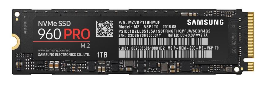
can be used simultaneously. Five versions of PCIe have been defined, with version 1
 supporting 2.5 giga-transfers per second (GT/s) per lane, version 2 at 5 GT/s, version
 3 at 8 GT/s, version 4 at 16 GT/s, and the upcoming version 5 expected to run at 32
 GT/s per lane. Today’s implementations are embodiments of version 4.

 When SSDs started to become a part of high-performance enterprise systems, it was
 only natural that storage designers looked to PCI as a way to harness all of the
 bandwidth that NAND flash could offer. Unfortunately, there was no standard
 command protocol for storage on the PCI bus, so RAID cards, HBAs, and SSDs from
 different manufacturers each communicated differently, with commands loosely based
 on an AHCI protocol but with differences that prevented original equipment
 manufacturers from using multiple manufacturers as alternate sources for products.

 Intel stepped in and created the NVMe protocol not only to support the use of the PCIe
 bus for storage but also to optimize the protocol to make the most of both NAND flash
 and other memory technologies such as DRAM, MRAM, PCM, and more. Figure 14
 shows an M.2 form factor NVMe SSD.

 Figure 14. An M.2 form factor NVMe storage device. (Courtesy of Samsung.)

 The NVMe protocol focuses on high performance through updates to AHCI commands
 that were limited due to cost considerations when the specification was originally
 written in 2005. The AHCI command set was designed to allow a PCI-based HBA to
 control multiple HDDs and was not defined to make the best use of flash-based (or
 faster) storage. One good example of the differences between these two specifications
 is NVMe’s support of 65,535 command queues (as opposed to AHCI’s support of a
 single queue), with 65,535 outstanding commands supported per queue (compared to
 AHCI’s 32). Parallelism and multiple threads are supported without locking in NVMe,
 whereas AHCI could support this kind of traffic only through the use of a lock.

 In brief, NVMe provides a better match between the parallel processes in the CPU and
 the parallel nature of solid-state storage than did its more serial-oriented
 predecessors, while the PCIe interface supports extremely high bandwidth.

 Memory Channel
 Because the fastest interface to the CPU is the memory channel, there have been a
 few efforts to bring storage to this bus and outperform the NVMe/PCIe interface. Two
 of these have been given the names NVDIMM-N and NVDIMM-F.

23
An NVDIMM-N is similar to a standard registered DIMM (RDIMM) but with the addition
 of a NAND flash chip that stores the DRAM’s data in the event of a power failure. This
 makes the DIMM nonvolatile or persistent, and persistence is a key attribute of
 storage. Because the memory on an NVDIMM-N can be treated as storage,
 application programs that focus on data integrity can use an NVDIMM-N as an
 extremely fast form of storage. An NVDIMM-N is roughly 1,000 times as fast as an
 SSD.

 This comes at some expense. The NVDIMM-N not only contains the components of a
 standard RDIMM; it also requires an external supercapacitor to provide the energy
 that allows the NVDIMM to perform its backup sequence while the rest of the system
 is shutting down (Figure 15). A controller has the job of moving the DRAM’s data into
 the NAND flash after a power failure as well as restoring the data from the NAND back
 into the DRAM once power is regained.

 Figure 15. An NVDIMM-N block diagram. (Objective Analysis, 2017.)

 But the DRAM is connected to the server’s memory bus and so must be disconnected
 before the NAND and controller chips can talk to the DRAM. A number of high-speed
 multiplexer chips connect the DRAM, either to the memory bus or to the NAND flash
 chip. These multiplexers are right in the middle of the server’s most critical speed path,
 so they must be very fast, because any delay in the multiplexer will slow down the
 DRAM. This, plus the fact that a faster DRAM chip must be used, drives up the cost
 of the NVDIMM-N significantly.

 The NVDIMM-F is a very different way to use the DRAM bus than is the NVDIMM-N.
 Just as HBAs can be used to attach multiple HDDs or SSDs to the PCIe bus, the
 NVDIMM-F uses a controller similar to the kind used in an HBA to connect multiple

24
SSDs to the DRAM bus. Although this approach drew a lot of interest in 2014–2015,
 its benefits did not live up to expectations, and the idea has since been abandoned by
 its supporters. It appears that the lack of an interrupt mechanism on the double data
 rate 3 (DDR3) and DDR4 buses unacceptably limited this approach’s performance.

 Table 1 compares these various memory and storage interface technologies.

 Table 1. A comparison of storage interfaces.

 Interface Mnemonic Application Transfer Characteristics
 Meaning Speed
 SATA Serial ATA HDD/SSD interface Up to 16 Low cost and
 Gb/s performance
 Bus overhead >1 µs
 SAS Serial Device and Up to 24 Supports multiple
 Attached subsystem Gb/s ports
 SCSI Interface Error detect and
 correction
 FC Fibre Device and network Up to Predominately SCSI
 Channel subsystem 128 Gb/s commands and
 interface features
 NVMe Nonvolatile Connection 32 GT/s Up to 32 lanes
 memory of peripheral per lane High command queue
 express over devices including support
 PCie SSDs
 NVDIMM Nonvolatile Memory Up to 4 Very low latency
 memory on Sometimes used GT/s No interrupts
 memory for storage over a Deterministic
 channel 64-b bus

 Network Interfaces: Ethernet, Infiniband, and NVMe-oF
 Today’s virtualized systems are built using clusters of servers that communicate with
 shared storage. This allows any process to be run on any of the servers in the cluster
 and to share data sets that are in the shared storage pool, all of which vastly improve
 efficiency over systems with servers and storage devoted to a single task.

 Such systems require a high-speed network to connect these servers to the shared
 storage. Different networks are used to satisfy different storage requirements, with
 Ethernet and InfiniBand broadly deployed in today’s systems and NVMe over fabric
 (NVMe-oF) being defined for future use.

 The following sections briefly describe each of these.

 Ethernet
 Ethernet is the mainstay of data-center communications, having provided good
 performance and economy since 1980. The interface has evolved over time from 2.94

25
Mb/s over coaxial cable to today’s 10 Gb/s over more economical twisted-pair cables.
 Data-center backbones include 40-Gb and even 100-Gb Ethernet over fiber. Note that,
 when 10-Gb/s Ethernet was first introduced, it was supported only on optical fiber and
 later was made to work over twisted pair, so it’s quite possible that future
 developments will support 100-Gb/s communication over twisted-pair copper wires.
 Like the SATA, SAS, and PCIe standards discussed earlier, Ethernet uses two
 differential signal pairs, one pair for transmit and one pair for receive.

 The standard’s four greatest strengths are its economy, widespread use, support of
 long copper cable lengths (up to 100 m), and reliability, having been field proven for
 nearly four decades. Where Ethernet loses out to other network protocols is in those
 applications for which bandwidth and/or latency are sufficiently important to justify
 shorter cable lengths and higher costs.

 InfiniBand
 InfiniBand is a higher-performance short-haul network widely used in supercomputers.
 This network, introduced in 1999, is used for backend server connections, often as
 part of external storage systems.

 InfiniBand supports channels of four, eight, or 12 links, each with a signaling rate of
 up to 10 Gb/s (for quad data rate) over copper or 25.7 Gb/s for fiber optic. Each link
 consists of one differential pair of inputs and one differential pair of outputs.

 The latency of InfiniBand is less than 20% that of 10-Gb Ethernet at fewer than 2 µs
 compared to the 12.5 µs of 10-Gb Ethernet. (The latency for 1-Gb Ethernet ranges
 from 29 to 100 µs.) Both copper and optical fiber interconnects are supported by
 InfiniBand, with copper cable lengths limited to 10 m and fiber supported in lengths up
 to 10 km.

 InfiniBand is less widely used than Ethernet, and it employs a wider interface with
 more costly connectors. These all serve to drive its price much higher than that of
 Ethernet.

 NVMe-oF
 Now that NVMe has gained acceptance and is being widely used for PCIe SSDs, it is
 only natural that the industry is investigating other ways to use the protocol to
 accelerate storage interfaces. The protocol’s deep queues and solid architecture make
 it suitable for communications between two asynchronous devices, such as two
 servers in a data center. The protocol’s queueing structure allows deep queues to act
 as shock absorbers for traffic between servers, giving the traffic a place to wait until
 the system on either side frees up for communication.

 The NVMe-oF topology can be used with Ethernet or InfiniBand, and it is sometimes
 also used with other interfaces, such as Fibre Channel. This interface can also be
 used to allow computers access to each other’s storage via a remote direct-memory-
 access (RDMA) approach rather than through conventional I/O methods. This means
 that one computer can access another computer’s memory as if that memory actually
 resided within the first computer—which is especially useful when shared data that
 must be accessed by the first computer are stored within the second computer’s
 persistent memory.

26
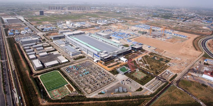
Because RDMA does not go through the operating system’s I/O stack, it can run at
 speeds closer to the speed of memory. Naturally, this could create conflicts unless the
 servers were synchronized, a possibility that could slow down all the servers in the
 cluster. NVMe’s queueing structure allows asynchronous systems to communicate
 efficiently without having to be synchronized with one another.

 Business Trends for Storage and Memory Devices

 The digital memory and storage industry is a very dynamic one. Nonvolatile memories
 are poised to replace volatile memories, making memory persistent. This will lead to
 big changes in firmware and computer architecture. Faster persistent memories will
 ultimately be an important element in future memory or data-centric computing in
 which the processing is disaggregated and brought closer to the locations where data
 are stored rather than moving increasingly large data sets back and forth from central
 processors. The latter approach is common today and results in latencies in
 processing data as well as considerable energy expended to move the data to and
 from processors. Some emerging nonvolatile memory technologies, such as MRAM,
 could even be part of spintronic processing systems, where the processing element is
 intimately connected to the memory being processed.

 Capital Investments, Regional Developments, and Industry
 Consolidation
 The huge growth in digital storage demand is creating great interest in storage and
 memory technologies of every type. The HDD industry has experienced considerable
 consolidation, to the point that there are only three manufacturers of HDDs (Seagate
 Technology, Western Digital, and Toshiba) and a small number of subcontractors and
 component manufacturers (such as Broadcom, Marvell, MMI, NHK, Nitto Denko,
 Showa Denko, and TDK/SAE).

 Likewise, the magnetic tape market looks as though it has narrowed to support the
 LTO tape format, with likely one contract manufacturer of tape drives and two suppliers
 of tape media (Fujifilm and Sony). The LTO program participants are Atmel, Fujifilm,
 HPE, IBM, Imation, Maxwell, Mountain Engineering, NXP Semiconductors, Quantum,
 Sony, Spectra Logic, TDK, Teijin Dupont Film, and Toray Industries. These magnetic
 storage companies have facilities all over the world and, in particular, in Asia and North
 America.

 While current HDD and magnetic tape manufacturing capacity is sufficient to meet
 demand storage capacity growth for several years, the demand for NAND flash
 memory is exploding. This is leading to intense investments by the largest established
 flash manufacturers (Samsung, Toshiba, Western Digital, Intel, Micron, and SK Hynix)
 as well as entry into the market by new players, particularly in China.

 NAND flash chips have been manufactured by Intel Corporation and Micron
 Technology through a joint venture in the United States. Micron has another plant in

27
You can also read