A Customized On-die Oscilloscope for Monitoring of Noise Waveforms inside IC Due to ESD
←
→
Page content transcription
If your browser does not render page correctly, please read the page content below
IDEC Journal of Integrated Circuits and Systems, VOL 8, No.2, April 2022                                                                       http://www.idec.or.kr

            A Customized On-die Oscilloscope for Monitoring of
                  Noise Waveforms inside IC Due to ESD

                 Zakirbek Mamatair uulu 1 Jung Hoon Cho2, Sang Yeong Jeong3 and Jin Gook Kima
                                              School of ECE, Ulsan National Institute of Science and Technology
                                     E-mail : 1zakirbek@unist.ac.kr, 2jhooncho@unist.ac.kr, 3sangyeong@unist.ac.kr

   Abstract - An on-die oscilloscope circuit is proposed to
monitor the power noise waveforms inside IC due to the
electrostatic discharge (ESD) events for a more complete
analysis of the effects of the ESD on the electronic systems.
When an ESD event occurs, the induced noise voltage
waveform in the power supply is sampled and converted to
digital data in real time. A holding signal created by the ESD
detector circuit is used to hold the digital data. The stored
digital data are read and converted back to the analog noise
waveform based on the sampling process. The operation of each                          Fig. 1. The on-die oscilloscope for monitoring of power supply noises inside
circuit block in the monitoring IC is analyzed and validated by                        IC in an electronic system.
measurement results. The delay between eight clock signals
from the DLL is about 200ps for 620MHz input clock as                                  modeling system-level ESD noises in the wearable devices
expected. The power noise waveforms due to the ESD events
                                                                                       using the ESD discharging currents.
are measured with a digital oscilloscope instrument using
cables and directly sampled by the on-die oscilloscope with a                             In all of these proposed papers, the ESD noises inside
sampling rate of 5GHz and 1.6GHz. These sampled noises are                             electronic products were studied in the same way by
converted and reconstructed into analog noise waveforms, and                           measuring the ESD noise voltage waveforms with an
then compared to the noises measured by the digital                                    oscilloscope using cables. However, this measurement
oscilloscope.                                                                          method has some limitations and issues. First, soldering the
                                                                                       measurement cables to the interested nets could be
  Keywords—Analog-to-Digital     Converter(ADC),      Binary                           sometimes infeasible in a smaller and denser product.
counter, Delay Locked Loop(DLL), Electrostatic Discharge                               Second, the measured differential-mode voltages can be
(ESD), ESD detector, Linear regulator, Monitoring IC, On-die
                                                                                       affected by the common-mode noises due to the strong
oscilloscope, Reconstruction, Sampling, Shift register,
Transmission line pulse (TLP)                                                          radiation from the ESD generator. Third, when measuring
                                                                                       the ESD noise waveform, it can be different from the actual
                                                                                       ESD noise waveform inside IC because the radiated field can
                              I. INTRODUCTION                                          affect the measurement cables, wire bonding, and
                                                                                       oscilloscope. Fourth, parasitic resistance, inductance, and
   ESD events can be easily generated by human activities
                                                                                       capacitance of PCBs and cables can affect measured
[1] and cause various failures in an electronic system. For
                                                                                       waveforms, and the longer the path from the event origin to
the safety of the product and customers, ESD issues should
                                                                                       the measuring device, the greater the problems.
be considered early in the design phase of the product.
                                                                                          Several studies have been proposed to solve these
Therefore, the ESD immunity test according to international
                                                                                       mentioned measurement limitations. In [6], the ESD
standards [2] has to be implemented on every electronic
                                                                                       detection circuit is proposed to approximate the levels of
product. In [3], the effect of ESD noises on the mobile
                                                                                       noises due to ESD events. The melted fuse is used to sense
phones was analyzed by checking the immunity of these
                                                                                       the ESD noises, which have levels above the threshold level,
devices to ESD events, and the ESD immunity was improved
                                                                                       by the ESD detector. In [7], the on-chip detector circuit uses
by using RC low pass filters. The electromagnetic
                                                                                       inside capacitors to sense ESD noises which are coupled to
susceptibility (EMS) problems due to ESD in IC were
                                                                                       on-die capacitors. In [8], an RC circuit is used inside the on-
studied in [4]. In [5], the soft failures in the operation of
                                                                                       chip detector to sense the ESD noises. These all on-die
wearable devices due to the ESD events were studied by
                                                                                       detector circuits can provide only limited information, such
a. Corresponding author; jingook@unist.ac.kr                                           as peak voltages or current levels of ESD noises, without any
                                                                                       precise information about the actual ESD noise waveforms.
Manuscript Received Dec. 27, 2021, Revised Mar. 21, 2022, Accepted
Mar. 30, 2022                                                                          In [9], the IC is proposed to monitor ESD noise waveforms.
                                                                                       However, this circuit design failed to monitor ESD noise
This is an Open Access article distributed under the terms of the Creative Commons     waveforms as expected in a real experiment. In this paper,
Attribution Non-Commercial License (http://creativecommons.org/licenses/bync/3.0)
which permits unrestricted non-commercial use, distribution, and reproduction in any   an on-die oscilloscope circuit is proposed to overcome
medium, provided the original work is properly cited.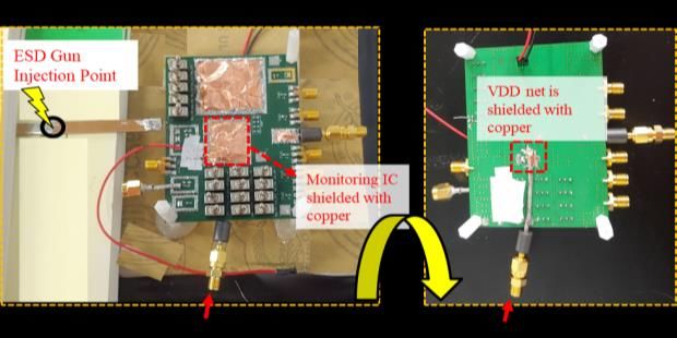
IDEC Journal of Integrated Circuits and Systems, VOL 8, No.2, April 2022                                                         http://www.idec.or.kr

limitations due to the measurement methods using cables                    shift register are converted back to an analog noise
and digital oscilloscope by directly capturing the ESD noise               waveform through post-processing which is based on the
waveforms inside IC in a convenient way within a                           sampling process and the attenuation ratio.
considerable short path for a more complete investigation of
the effects of the ESD events on the electronic products, as
shown in Fig. 1.
   Section II discusses the block diagram of the proposed on-
die oscilloscope and explains the operations of circuit blocks
when monitoring ESD noises. In section III, the operations
of circuit blocks inside the on-die oscilloscope are tested in
the experiment. Moreover, the ESD noise waveforms are
measured by the oscilloscope using cables and directly
sampled by the on-die oscilloscope, and these measured
waveforms by the oscilloscope and reconstructed analog
noise waveforms by the monitoring IC are compared with                            Fig. 2. Block diagram of the proposed on-die oscilloscope.
each other.

II. ANALYSIS OF OPERATION OF EACH CIRCUIT BLOCK IN THE                                      III. RESULTS AND DISCUSSIONS
                         ON-DIE OSCILLOSCOPE
                                                                           A. Designed IC and PCB Structures
   The overall block diagram of the proposed on-die
oscilloscope is shown in Fig. 2. The main building blocks of                 The designed monitoring IC was fabricated in a 180nm
the system are the linear regulator, the delay locked loop                 CMOS process, and its total size is 5,000μm × 3,916μm.
(DLL), 8 flash type analog-to-digital converter (ADC), shift               The location of each circuit block in the designed monitoring
register, binary counter, and ESD detector. An ESD event                   IC is shown in Fig. 3.
applied to the power supply net VDD is shown as a "spark"
at VDD. For the correct operation of circuit blocks inside the
on-die oscilloscope, the linear regulator is used to create a
new stable internal power supply VDDA, which must be
robust against the ESD noises in the external power supply
VDD. For matching the power noise waveforms in the VDD
to the sampling range of the ADCs resistive voltage division
is used to attenuate the DC parts of the noise waveforms at
the (3.3:0.8) ratio and capacitive voltage division is used to
attenuate the AC parts of the noise waveforms at the (2.5:1)
ratio. The high speed for sampling the high frequency
components of the noise waveforms is achieved by
combining eight ADCs so that the effective sampling rate is
                                                                              Fig. 3. Designed monitoring IC and locations of each circuit block.
increased by 8 times, and by using the DLL which can
provide eight multi-phase high frequency clock signals to
eight ADCs for sampling. Each ADC samples and converts                         In Fig. 4(a), the designed monitoring IC is mounted on a
the attenuated noise waveform into 5-bit digital data. This                6-layer PCB with dimensions of 91mm × 68mm by chip-
proposed on-die oscilloscope requires a high-speed sampling                on-board (COB) assembly. The first layer is used for
rate of at least 5 GHz to accurately sample high-frequency                 mounting the designed monitoring IC and electrical
power noise, such as ESD noise. Flash ADCs with higher                     components, the second and sixth layers are for the ground
sampling rates are preferred over other types of ADCs with                 planes, and the fifth layer is used for the 3.8V DC VDD
higher bit resolution but slower speeds, as its main study is              power plane to supply the monitoring IC. The fourth layer is
on high- frequency power noise. Flash ADC resolution was                   divided into two planes, the first is the ground plane, and the
only 5 bits, but it was sufficient to capture power noise                  second is the 3.3V power plane, which is used to generate
accurately. The sampled digital data from ADCs are                         the reference clock signals for the DLL by supplying an
shifted into the shift register, which consists of 128 5-bit D             oscillator and a clock buffer on the PCB. The important
flip-flops (DFFs) storing binary bits. In the shift register,              signal traces for the input or output signals of the monitoring
sampled data from each ADC are continuously shifted and                    IC are routed in the third layer with a characteristic
lost in the last 5-bit DFFs. A Hold signal is used to stop the             impedance of 50 Ω. Two commercial regulators are mounted
data shift inside the shift register. Hold signal is sent to the           on the PCB to generate a 3.8V DC VDD power supply and
register from the ESD detector circuit when it senses the                  a 3.3V DC power supply from 5.4V DC voltage supplied
occurrence of ESD noises. After the data shift is stopped, the             from outside. The input signal Read_CLK is for providing a
binary counter is used for reading the data from the first 5-              reference clock signal to the binary counter of the monitoring
bit DFF to the 128th 5-bit DFF per every reference clock                   IC. Two output signals of the IC (MUX_OUT and
pulse supplied from outside. The digital data read from the                CLK_LATCH) are measured by the digital oscilloscope to
                                                                           study the performance of the DLL and are terminated to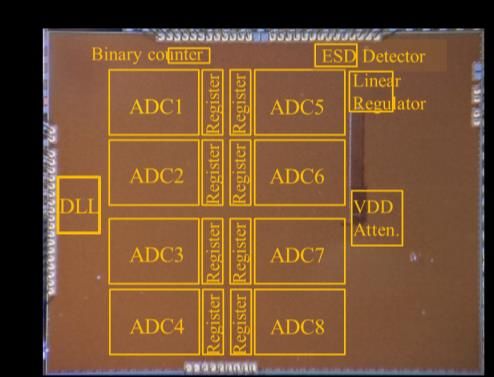
IDEC Journal of Integrated Circuits and Systems, VOL 8, No.2, April 2022 http://www.idec.or.kr
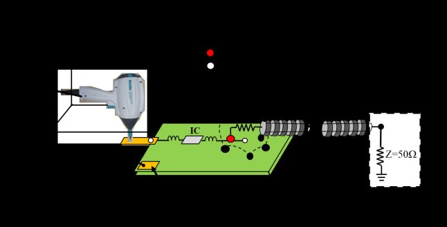
ground through 50 Ω resistors on the PCB for impedance B. Experiment of ESD Detector
matching. For triggering the oscilloscope to start measuring
In this section, the performance of the ESD detector
the output data from the registers the output signal A7, the
circuit block is analyzed when a noise occurs in the VDD by
LSB of the 7-bit binary counter is measured. The output
applying transmission line pulse (TLP) toward the VDD net
Hold signal is measured to study the ESD detector when
on the PCB, as shown in Fig. 5. Most of the applied TLP
ESD events occur. For checking the stability of the internal
signal is reflected because the input impedance of the power
VDDA power supply inside the monitoring IC the output
supply VDD net on the PCB is very small compared to 50 Ω.
VDDA net is measured on the PCB. The 5-bit data stored in
It is possible to control the amplitude and width of the TLP
each of the 128 5-bit DFFs in the shift register are read in the
signal by adjusting the charging voltage (Vc) and the pulse
proper sequence from the 5 output nets (OUT1 to OUT5) on
width (Td) from the TLP generator.
the PCB when the binary counter starts to operate. Because
When the ESD detector circuit senses noise in the VDD,
these output signals are generated by the large size inverter
it changes the initial low state of the Hold signal to a high
buffers which have low output impedances, they are
state to stop the data shift in the register. When the TLP
measured using the semi-rigid cables that are connected to
signal with the 5ns pulse widths and charging voltage (Vc)
these output nets in series with 470 Ω to create a 520 Ω high
of 140V is applied, the noise with 0.890V amplitude is
impedance probe, as shown in Fig. 4(b). These output signals
created in the VDD, as shown in Fig.6. A charging voltage
are measured with a digital oscilloscope and compensated
(Vc) of at least 140 V is required for the ESD detector to
for the 520 Ω high impedance probe gain by multiplying
sense the noise in the VDD and make the high Hold signal.
these signals by 10.4.
If a charging voltage is below 140V, the noise created in the
VDD is not sensible by the ESD detector. From the
measurement result, it is shown that the ESD detector circuit
can sense all noises in the VDD which have amplitudes
higher than 0.890V.
(a)
Fig. 6. Measured voltage waveforms of VDD and Hold signals when the
TLP signal with the 5ns pulse width and charging voltage of 140V (Vc) is
applied.
C. Experimental Validation of Stability of Internal Power
The stability of the internal supply voltage VDDA in the
presence of external noise in the VDD is required for the
correct operation of the monitoring IC. The power supply
rejection ratio (PSRR) of the linear regulator inside IC is
(b) shown in Fig. 7. It was confirmed that the linear regulator
can block higher frequency noises more effectively. The
Fig. 4. (a) Designed PCB, measurement cables, and components on the stability of the VDDA is validated by measuring both the
PCB. (b) Setup for measuring important signals and powers.
internal supply voltage VDDA and the external supply
voltage VDD on the PCB when TLP signals are applied.
When a TLP signal with 10ns width is applied the
measurement results of the VDD and VDDA voltage
waveforms are shown in Fig. 8. Although there is a high
1.111V peak-to-peak noise voltage in the VDD, the noise
amplitude in the VDDA is lower than 130 mV peak-to-peak.
When two 1μF de-caps are installed between VDDA-GND
nets, as shown in Fig. 4(a), to make the VDDA supply net
more stable, the noise in the VDDA almost disappears. When
the monitoring IC is used for sampling ESD noises, de-caps
Fig. 5. Test setup for applying TLP signals. are installed between VDDA-GND nets to make the stable
VDDA net for the correct operation of the monitoring IC.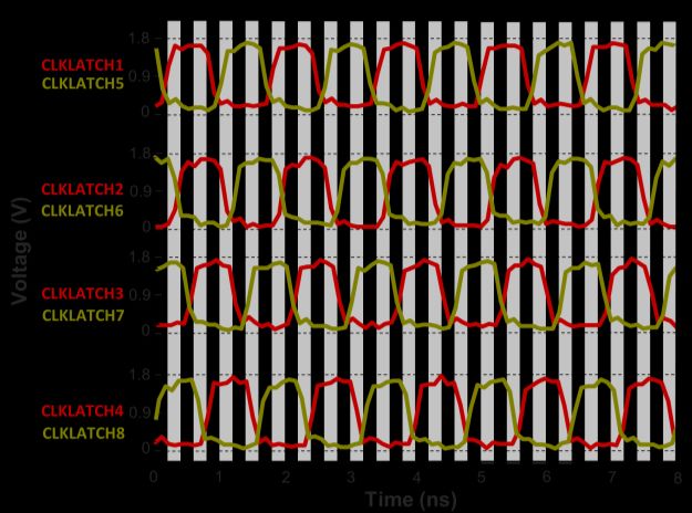
IDEC Journal of Integrated Circuits and Systems, VOL 8, No.2, April 2022                                                      http://www.idec.or.kr

                                                                              Fig. 9 shows the measurement results of all eight clock
                                                                           signals (CLKLATCH1 to CLKLATCH8) from the DLL with
                                                                           respect to the same reference clock. The delay of each clock
                                                                           signal from the previous clock signal is same with the
                                                                           expected 200ps (one eighth of the 620MHz clock signal
                                                                           period). Moreover, the measured rising time of the eight
                                                                           clock signals is short as expected, about 100ps. The total
                                                                           effective sampling rate of the monitoring IC is about 5GHz
                                                                           because eight ADCs with 620MHz input clocks are
                                                                           implemented to sample the ESD noise waveforms.

               Fig. 7. Simulated PSRR of the linear regulator

Fig. 8. Measured voltage waveforms of VDD and VDDA signals when the
applied TLP signal has 10ns pulse width.
                                                                                        Fig. 10. Block diagram of 5-bit flash ADC
D. Experimental Validation of DLL and ADC Operation.
                                                                              The block diagram of flash ADC is shown in Fig. 10. The
   When the monitoring IC is sampling ESD noises in the                    ADC is composed of a reference voltage ladder,
power supply VDD it uses 620MHz clock signals to sample.                   comparators, and a digital block including a gray encoder,
The oscillator and clock buffer on the PCB generate a                      gray to the binary converter, and the latch circuit. The 32-
620MHz clock signal, which is transferred as a reference                   reference voltages are created between VDDA and GND for
clock for the DLL inside the monitoring IC, and the DLL                    each comparator. The minimum reference voltage V_REFN
makes eight multi-phase 620MHz clock signals by using this                 and the maximum reference voltage V_REFP are designed
reference clock. These eight multi-phase 620MHz clock                      as 0.3V and 1.3V, respectively. Therefore, the ADC can
signals can be measured in the output CLKLATCH net on                      capture signals in the sampling range of 0.3V to 1.3V,
the PCB, in which the clock signal is selected from the eight              voltage gap is calculated as 31.3mV. The latch circuit is for
clocks (CLKLATCH1 to CLKLATCH8) by controlling a 3-                        adjusting skew that comes from the encoding and converting
bit switch on the PCB. The input clock of the first ADC is                 process. Each ADC consumes about 60mA current in root
also measured in the MUX_OUT net on the PCB as a                           mean square value.
reference clock to extract the delay between the eight clock
signals from the DLL by measuring the delay of each clock                  E ESD Experimental Test Setup
signal from the same reference clock.
                                                                              In the ESD immunity test of the electronic products, the
                                                                           effect of ESD is studied by injecting ESD discharge currents
                                                                           with the ESD gun, which generates strong electromagnetic
                                                                           radiation. Therefore, the test setup for conducting the ESD
                                                                           test is considered to reduce the influence of the ESD gun’s
                                                                           radiation on the operation of the monitoring IC. In the ESD
                                                                           experimental test setup, the ESD gun was placed inside a
                                                                           metal gate and important components on the PCB such as
                                                                           the monitoring IC, generator part, and measurement signals
                                                                           are shielded with copper tape as shown in Fig. 11(a). The
                                                                           ESD gun injects an ESD discharge current through the hole
                                                                           in the metal cage into the copper stick that connects to the
                                                                           VDD pad on the PCB. This ESD current creates the noise
                                                                           waveform in the VDD, which is then sampled by the
                                                                           monitoring IC. The same ESD noise waveform is also
Fig. 9. The measured results of eight 620 MHz multi-phase clock signals    measured with oscilloscope by soldering the semi-rigid
generated by the DLL.                                                      coaxial cable with ferrite beads to the VDD net on the PCB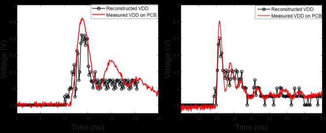
IDEC Journal of Integrated Circuits and Systems, VOL 8, No.2, April 2022                                                              http://www.idec.or.kr

next to the monitoring IC, as shown in Fig. 11(b). The                         (8×200MHz). The measured ESD noise voltage in the VDD
ground strap of the ESD gun, metal cage, and PCB ground
                                                                               agrees well with the reconstructed analog waveform by the
plane were connected to a reference ground plane (GRP) on
                                                                               on-die oscilloscope IC when the 1.6GHz sampling rate is
the floor in this ESD experimental test setup.
                                                                               used, as shown in Fig. 12(b). According to the attenuation
                                                                               ratio of DC and AC parts, when applied DC voltage is 3.8V
                                                                               as this ESD experiments, the peak VDD voltage that can be
                                                                               captured by the proposed on-die oscilloscope is 4.8V. This
                                                                               peak value on VDD occurs under 450V ESD events. VDDA
                                                                               which supplies power to DLL, ADC, and the inner part is
                                                                               protected by the linear regulator with de-caps, remained
                                                                               stable. Therefore, the peak ESD voltage value that can be
                                                                               captured by the proposed on-die oscilloscope depends on the
                                                                               sampling range rather than VDDA consideration.
                                        (a)

                                                                                                 (a)                                (b)
                                                                               Fig. 12. Measured ESD noise voltages on the PCB and the reconstructed
                                                                               waveforms by the on-die oscilloscope IC with (a) 5GHz sampling rate and
                                        (b)                                    (b) with 1.6GHz sampling rate.
Fig. 11. (a) Test setup for the ESD experiment. (b) Photographs of the front
and rear sides of the PCB in the ESD experiment.                                            TABLE I. Comparison with Previous Research
                                                                                                                       Resolution/        Measurement
F.ESD Experimental Results                                                        Ref.          Contribution          Sampling rate        Validation

   The ESD noise waveform in the VDD is sampled by                                        ESD event sensing in
                                                                                                                           Not
                                                                                  [8]     power supply voltage                                 Yes
ADCs and stored in registers. After the Hold signal from the                              using RC based circuit
                                                                                                                        applicable
ESD detector stops the shifting of data, a 10MHz read clock
                                                                                          Circuit design for noise
is applied through the input Read_CLK net to the binary                           [9]
                                                                                          waveform capturing
                                                                                                                        5bit/6.4G               No
counter inside the monitoring IC for reading the stored data
                                                                                          Reconstruction of the
in the shift register. The LSB of the 7-bit binary counter (A7)                  This
                                                                                          power noise waveforms          5bit/5G               Yes
triggers the oscilloscope to start measuring the 5 output nets                   work
                                                                                          inside IC
(OUT1 ~ 5). In every 10 MHz read clock cycle, digital data
from one 5-bit DFFs in the shift register is read through 5
output nets and in total, it takes 128 clock cycles (12.8μs) to                                          IV. CONCLUSION

read all data from the 128 5-bit DFFs. A set of the measured                      This paper proposed the on-die oscilloscope to analyze the
128 5-bit binary data is converted to an analog voltage                        effect of ESD on electronic products by monitoring the ESD
through post-processing and arranged along the                                 noise waveforms in a convenient way. The function of each
corresponding sampling time step of 200ps at the 5GHz                          circuit block in the on-die oscilloscope was discussed. The
sampling rate to reconstruct the noise signal duration of 26                   internal design of the manufactured monitoring IC and PCB,
ns. The DC and AC parts of this analog waveform result are                     and a setup for measuring important signals were explained.
then multiplied by the (3.3:0.8), and (2.5:1) ratio to                         The measurement showed that internal power noises in the
compensate the attenuation in the R-C attenuation circuit in                   VDDA can be removed totally by installing de-caps. The
Fig. 2.                                                                        operation of the DLL was checked by observing the
   In fig. 12(a), the ESD noise voltage in the VDD measured                    measurement results of eight multi-phase clock signals
by the digital oscilloscope shows sufficient agreement with                    generated by the DLL. The performance of the ESD detector
the reconstructed analog waveform by the on-die                                circuit was analyzed by observing the noise in the VDD and
oscilloscope IC after all post-processing. To reconstruct a                    Hold signal. A sufficient agreement between the ESD noise
longer ESD noise duration with the same 128 points, another                    waveforms measured by the digital oscilloscope using cables
200MHz reference clock is supplied to the DLL from the                         and the reconstructed ESD noise waveforms by the designed
generator part. In this time, the duration of 80ns of the same                 on-die oscilloscope proved that the on-die oscilloscope can
ESD noise waveform is reconstructed by the on-die                              be applied to conduct ESD immunity tests in complex
oscilloscope due to the low sampling rate of 1.6GHz                            integrated systems by installing this on-die oscilloscope IC
                                                                               next to the real electronic product.
IDEC Journal of Integrated Circuits and Systems, VOL 8, No.2, April 2022                                                http://www.idec.or.kr

                          ACKNOWLEDGMENT                                                           Jung Hoon Cho received the B.S.
                                                                                                   degree in electronic engineering
  The chip fabrication and EDA Tool were supported by the                                          from Gachon University, Seongnam,
IC Design Education Center (IDEC), Korea.                                                          Republic of Korea, in 2021. He is
                                                                                                   currently working toward the M.S.
                               REFERENCES                                                          degree in Ulsan National Institute of
                                                                                                   Science and Technology (UNIST),
[1] A. Talebzadeh, M. Moradian, Y. Han, D. E. Swenson and                                          Ulsan, Korea.
    D. Pommerenke, "Electrostatic charging caused by                                                  His research interests include
    standing up from a chair and by garment removal", IEEE                                         analog circuits design, electro-
    Symposium on Electromagnetic Compatibility and                         magnetic interference, and wireless power transfer.
    Signal Integrity, Santa Clara, CA, 2015, pp. 57-62.
[2] Road vehicles — Test methods for electrical disturbances
    from electrostatic discharge, ISO 10605 Ed. 2.0, July.                                         Sang Yeong Jeong received the B.S.
    2008.                                                                                          and Ph.D. degrees in electrical
[3] K. H. Kim and Y. Kim, “Systematic analysis                                                     engineering from the Ulsan National
    methodology for mobile phone's electrostatic discharge                                         Institute of Science and Technology,
    soft failures”, IEEE Trans. Electromagn. Compat., vol.                                         Ulsan, South Korea, in 2015 and
    53, no. 3, pp. 611- 618, Aug. 2011.                                                            2021, respectively. From March
                                                                                                   2021, he is currently working for the
[4] T. Ostermann, “ESD induced EMS problems in digital
                                                                                                   IC&EMC Laboratory at the Ulsan
    IOs,” in Proc. IEEE Nordic Circuits Syst. Conf.,
                                                                                                   National Institute of Science and
    NORCHIP Int. Symp. Syst.-on-Chip, Linkoping,
                                                                                                   Technology, Ulsan, South Korea, as
    Sweden, 2017, pp. 1–6.
                                                                           a postdoc fellow. His current research interests include
[5] J. Zhou et al., “Characterization of ESD risk for wearable             electromagnetic compatibility (EMC) problems in the power
    devices,” IEEE Trans. Electromagn. Compat., vol. 60,                   system and the noise reduction techniques by using
    no. 5, pp. 1313–1321, Oct. 2018.                                       integrated circuits (ICs).
[6] W. B. Kuhn, R. J. Eatinger, and S. A. Melton, “ESD
    detection circuit and associated metal fuse investigations                                     Jin Gook Kim (M’09-SM’15)
    in CMOS processes,” IEEE Trans. Device Mater. Rel.,                                            received his B.S., M.S., and Ph.D.
    vol. 14, no. 1, pp. 146–153, Mar. 2014.                                                        degrees in electrical engineering
[7] M. D. Ker, C. C. Yen, and P. C. Shih, “On-chip transient                                       from Korea Advanced Institute of
    detection circuit for system-level ESD protection in                                           Science and Technology, Daejon,
    CMOS integrated circuits to meet electromagnetic                                               Korea, in 2000, 2002, and 2006,
    compatibility regulation,” IEEE Trans. Electromagn.                                            respectively. From 2006 to 2008, he
    Compat., vol. 50, no. 1, pp. 13–21, Feb. 2008.                                                 was with DRAM design team in
[8] M. D. Ker and C. C. Yen, “Transient-to-digital converter                                       Memory Division of Samsung
    for system-level electrostatic discharge protection in                                         Electronics, Hwasung, Korea, as a
    CMOS ICs,” IEEE Trans. Electromagn. Compat., vol. 51,                                          senior engineer. From January 2009
    no. 3, pp. 620–630, Aug. 2009.                                         to July 2011, he worked for the EMC Laboratory at the
                                                                           Missouri University of Science and Technology, Missouri,
[9] W. Lee et al., "An On-die Oscilloscope for System-Level                USA, as a postdoc fellow. In July 2011, he joined the Ulsan
    ESD Noise Monitoring," 2019 IEEE International                         National Institute of Science and Technology (UNIST),
    Symposium on Electromagnetic Compatibility, Signal &                   Ulsan, Korea, where he is currently a professor. His current
    Power Integrity (EMC+SIPI), 2019, pp. 156-160.                         research interests include EMC, ESD, RF interference, and
                                                                           analog circuits design.
                               Zakirbek Mamatair uulu received
                               the B.S. and M.S. degrees in
                               electrical engineering from Ulsan
                               National Institute of Science and
                               Technology (UNIST), Ulsan, South
                               Korea, in 2019 and 2021,
                               respectively.
                                  His current research interests
                               include analog circuits design, ESD,
                               and wireless power transfer.

You can also read