A hybrid silicon evanescent laser with sampled Bragg grating structure based on the reconstruction equivalent chirp technique for silicon ...
←
→
Page content transcription
If your browser does not render page correctly, please read the page content below
Laser Physics

PAPER • OPEN ACCESS

A hybrid silicon evanescent laser with sampled Bragg grating structure
based on the reconstruction equivalent chirp technique for silicon
photonics
To cite this article: Ranzhe Meng et al 2021 Laser Phys. 31 065802

View the article online for updates and enhancements.

                               This content was downloaded from IP address 46.4.80.155 on 16/05/2021 at 20:18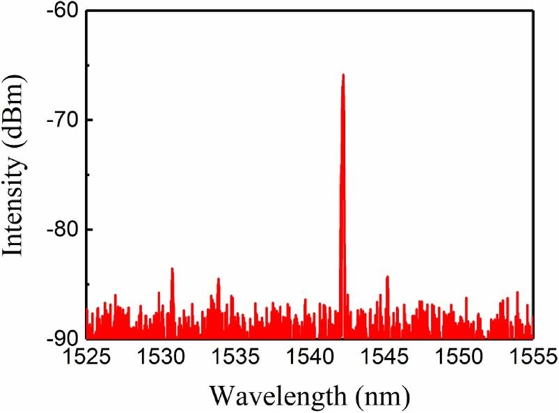
Astro Ltd                                                                                                                   Laser Physics

Laser Phys. 31 (2021) 065802 (4pp)                                                                                    https://doi.org/10.1088/1555-6611/abecde

A hybrid silicon evanescent laser with
sampled Bragg grating structure based
on the reconstruction equivalent chirp
technique for silicon photonics
Ranzhe Meng1,2,5, Hailing Wang1,5, Tao Shi1,3, Mingjin Wang1
and Wanhua Zheng1,2,3,4,∗
1
  Laboratory of Solid State Optoelectronics Information technology, Institute of Semiconductors,
Chinese Academy of Sciences, Beijing 100083, People’s Republic of China
2
  College of Future Technology, University of Chinese Academy of Sciences, Beijing 101408, People’s
Republic of China
3
  Center of Materials Science and Optoelectronics Engineering, University of Chinese Academy of
Sciences, Beijing 100049, People’s Republic of China
4
  State Key Laboratory on Integrated Optoelectronics, Institute of Semiconductors, Chinese Academy of
Sciences, Beijing 100083, People’s Republic of China

E-mail: whzheng@semi.ac.cn

Received 29 September 2020
Accepted for publication 19 January 2021
Published 28 April 2021

Abstract
In this paper, we report on a direct bonding hybrid silicon evanescent laser with sampled Bragg
grating structure based on the reconstruction equivalent chirp (REC) technique for the first time.
By the design of the REC technique, the hybrid silicon evanescent laser in the +1st order
channel is emitted. The optical mode is evanescently coupled between the III and V waveguide
and silicon waveguide. A laser with 24 mA threshold current and 0.3 mW output power from
silicon waveguide at 50 mA under the continuous wave operation is obtained.
Keywords: hybrid silicon laser, direct wafer bonding, sampled Bragg grating

(Some figures may appear in colour only in the online journal)

1. Introduction                                                                         integration will assume similar responsibilities as integrated
                                                                                        circuits in the future. Silicon photonics has its unique advant-
Large-scale photonic integrated circuits (PICs) have great                              ages, such as the compatibility of silicon photonics plat-
potential to overcome information transmission bottlenecks                              forms with the complementary metal oxide semiconductor
and will become the core of low-loss, high-performance and                              processes. The integration of high-performance light sources
high-speed data transmission systems. Large-scale photonic                              is a major challenge for silicon PICs due to the inherent lack
                                                                                        of light-emitting functions on silicon-on-insulator (SOI) sub-
                                                                                        strates. There have been some developments in Si Raman
5
∗
    Ranzhe Meng and Hailing Wang are co-first authors.                                  lasers and Ge lasers in recent years [1, 2], even efficient
    Author to whom any correspondence should be addressed.                              light emission from direct-bandgap hexagonal SiGe alloys is
                                                                                        demonstrated [3]. However, Si Raman lasers and Ge lasers
                   Original content from this work may be used under the terms          are optically pumped, and the hybrid silicon laser which is
                   of the Creative Commons Attribution 3.0 licence. Any fur-
ther distribution of this work must maintain attribution to the author(s) and the       integrated with InP and silicon substrates has its significant
title of the work, journal citation and DOI.                                            advantage in laser performance and PICs. Electrically-pumped

1555-6611/21/065802+4$33.00                                                         1                                     © 2021 Astro Ltd   Printed in the UK
Laser Phys. 31 (2021) 065802                                                                                                      R Meng et al

strong optical gain coefficients and mature optical gain coup-
ling schemes is beneficial for high output power and low
threshold current. Therefore, hybrid silicon lasers are a great
proposal for light sources in PICs.
    Laser sources integrated in PIC can be achieved using
various integration routes including flip-chip bonding [4],
benzocyclobutene (BCB) bonding [5, 6], direct wafer bond-
ing, and epitaxial growth. Since Fang et al demonstrated the
first hybrid silicon evanescent laser with a direct bonding pro-
cess in 2006 [7], the hybrid silicon laser could run under con-
tact conditions, They reported an electrically pumped distrib-
uted feedback (DFB) silicon evanescent laser in 2008 [8], and
a low threshold and high speed short cavity DFB hybrid sil-
icon laser was achieved in 2014 [9]. Recently, the sampled
Bragg grating (SBG) structure based on the reconstruction
equivalent chirp (REC) technique has been proposed in InP
laser arrays, whose wavelength spacing is 100 GHz [10, 11],                          Figure 1. The transmission of the SBG.
and the REC technique is an equivalent phase shift tech-
nique in the SBG structure, an equivalent π phase shift can
be introduced to ensure single mode lasing. The advantage
of the SBG structure based on the REC technique is that
50 GHz/100 GHz wavelength spacing can be achieved through
photolithography, while DFB grating cannot. In this paper,
we demonstrate a hybrid silicon evanescent laser with REC
technique. This structure is designed and fabricated on sil-
icon waveguide to select optical mode and form a hybrid laser
oscillating cavity, and the optical power output from the sil-
icon waveguide in the +1st order channel reaches 0.3 mW,
and the threshold current is 24 mA under the continuous
wave operation at room temperature. With a fixed seed grat-
ing, a multi-wavelength laser array can be obtained by vary-
ing the sampled period. In the future, we can achieve multi-
wavelength hybrid silicon laser arrays with 50 GHz/100 GHz
wavelength spacing by using the SBG based on the REC
technique.

2. Principle and device design

In a hybrid SBG silicon structure based on the REC tech-
nique, there are many sub-gratings [10, 11]. The lambda of             Figure 2. (a) Cross-sectional schematic structure of the hybrid
                                                                       silicon evanescent laser, (b) side view of the hybrid silicon
+1st order sub-grating is given by                                     evanescent laser.

                                  2neff Λ0 P
                          λ+1 =                             (1)        where κ0 is the coupling coefficient of the 0th order grating,
                                   Λ0 + P
                                                                       and ∆n̄eff is the perturbation by the grating corrugating, λ0 is
where P is the sampling period, Λ0 is the period of the uni-           the 0th order wavelength. While the coupling coefficient cor-
form seed grating, and neff is the effective refractive index of       responding to the +1st order sub-grating is
the hybrid waveguide. This principle is very similar to quasi-
                                                                                                       sin(πγ2 ) −iπγ2
phase matching in nonlinear materials for high efficiency light                            κ+1 = κ0             e      .                  (3)
wavelength conversion. Figure 1 shows transmission of the                                                  π
SBG. This structure can effectively suppress the lasing in its            In the equation, γ 1 and γ 2 are the duty cycle of the seed
0th channel, while the +1st channel can be located in the gain         grating and the sampled grating, respectively. Therefore, gen-
spectrum. Moreover, according to coupled mode theory, grat-            erally speaking, +1st channel of the SBG reduces the κ value
ing coupling coefficient κ is expressed as                             to 1/π of the normal DFB grating.
                                                                          Figure 2(a) shows cross-sectional schematic structure of the
                               2∆n̄eff                                 hybrid silicon evanescent laser, and figure 2(b) Side view of
                        κ0 =           sin γ1 π             (2)
                                λ0                                     the hybrid silicon evanescent laser. The device is fabricated

                                                                   2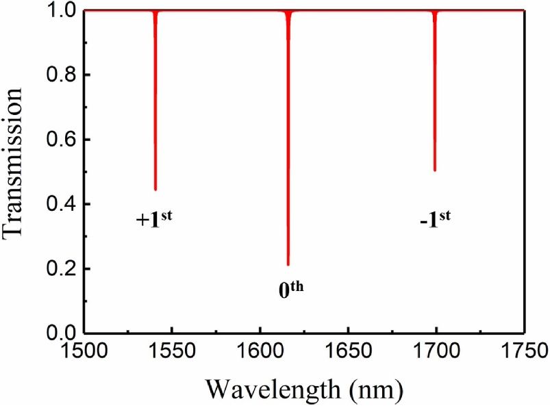
Laser Phys. 31 (2021) 065802                                                                                                      R Meng et al

Figure 3. Simulated cross-section optical mode profile of the
fundamental TE mode in the hybrid waveguide.                                           Figure 4. The structure of three tapers.

with a III–V epitaxial wafer and an SOI wafer with a 340 nm
top silicon layer and a 2 µm buried oxide layer. Gratings are
etched into the silicon waveguide, and III–V layer stack has
eight strained InAlGaAs quantum wells (QWs) with graded
index separate confinement hetero-structure layers.
    Figure 3 shows the simulated optical mode profile of the
fundamental transverse electric (TE) mode in the hybrid wave-
guide. The optical mode is confined in the silicon wave-
guide, and the grating on the silicon waveguide can provide
a strong grating coupling coefficient. The confinement factor
is 38% in the silicon waveguide, and 5.32% in the mul-
tiple QW (MQW) region, and a coupling coefficient κ+1 of
∼75.54 cm−1 is provided by the grating on silicon. The length
of the grating Lg is 400 µm, and κ+1 Lg value of the REC cavity
is 3.02.
    The structure of taper tapers on the hybrid silicon laser is        Figure 5. The L–I–V curve of the hybrid silicon laser at room
shown in figure 4, requiring a total taper length of ∼90 µm.            temperature.
Because the accuracy of the lithography machine is only
0.8 µm, 4 µm wide P-InP waveguide is tapered back to
0.8 µm, where MQW taper starts, allowing a 1.5 µm mar-
                                                                        dies were soaked acetone and isopropanol solution at 150 ◦ C
gin of the N-InP and MQW levels for fabrication tolerance
                                                                        to clean the surface of dies [13, 14]. The two die pieces are
purpose. The lengths of the P-InP taper, MQW taper and
                                                                        then brought into contact and annealed at 300 ◦ C in an almost
n-InP taper are 20 µm, 80 µm and 10 µm, respectively,
                                                                        vacuum environment for 10 h under a uniaxial pressure of
and the optical mode is pushed more into the silicon wave-
                                                                        1.5 MPa to complete the bonding process [15]. After selective
guide [12]. The simulations show that 80% of the funda-
                                                                        removal of the III–V materials, the III–V stack requires three
mental mode in the hybrid waveguide will couple to the silicon
                                                                        steps of etching to form III–V ridge waveguide, lead to N–InP
waveguide.
                                                                        electrode and isolate the near lasers, respectively. Before each
                                                                        etch, a layer of 300 nm SiO2 mask is deposited on the III–V
3. Fabrication and experimental results                                 stack. At the same time, three tapers on both sides of the III–
                                                                        V stack are also etched. The III–V ridge waveguide width is
The grating is formed by patterning with electron-beam litho-           4 µm wide and P-type contact window width is 2 µm. Ti/Au
graphy and inductively coupled plasma dry etching to form a             metal stack was deposited as contact metals for p- and n-type
28 nm depth surface corrugated grating with a 252 nm seed               contacts [16].
grating period and an around 5 µm sampled grating period                    After the hybrid silicon laser was driven by a positive bias
on the silicon ridge waveguide, and the silicon ridge wave-             voltage to the P contact, the light-current and current–voltage
guide is formed by patterning with lithography, which has a             characteristics of the hybrid silicon laser was measured by col-
width and ridge depth of 1.5 µm, and 200 nm, respectively.              lecting light out of one side of the laser into a calibrated integ-
The III–V stack is transferred to SOI wafer with a low temper-          rating sphere, and an optical spectrum analyzer was used to
ature hydrophilic bonding technique and processed for current           measure the spectrum data. It can be seen from figure 5 that
injection. For direct wafer bonding, the native oxide on the III–       the threshold current of the hybrid silicon laser is 24 mA, and
V stack and SOI dies are removed by dipping both dies in HF             the maximum output power is up to around 0.3 mW at room
aqueous solution for 20 s at room temperature, and the two              temperature.

                                                                    3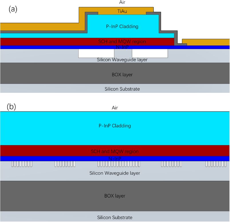
Laser Phys. 31 (2021) 065802 R Meng et al
References
[1] Jalali B, Raghunathan V, Dimitropoulos D and Boyraz O 2006
Raman-based silicon photonics IEEE J. Sel. Top. Quantum
Electron. 12 412–21
[2] Jurgen M et al 2012 An electrically pumped Ge–on–Si laser
National Fiber Optic Engineers Conf. PDP5A.6
[3] Fadaly E M T et al 2020 Direct-bandgap emission
from hexagonal Ge and SiGe alloys Nature
580 205–9
[4] Tanaka S, Jeong S-H, Sekiguchi S, Kurahashi T, Tanaka Y and
Morito K 2012 High-output-power, single-wavelength
silicon hybrid laser using precise flip-chip bonding
technology Opt. Express 20 28057–69
[5] Dhoore S, Li L, Abbasi A, Roelkens G and Morthier G 2016
Demonstration of a discretely tunable III-V-on-silicon
sampled grating DFB laser IEEE Photonics Technol. Lett.
28 2343–6
[6] Dhoore S, Rahim A, Roelkens G and Morthier G 2018 125
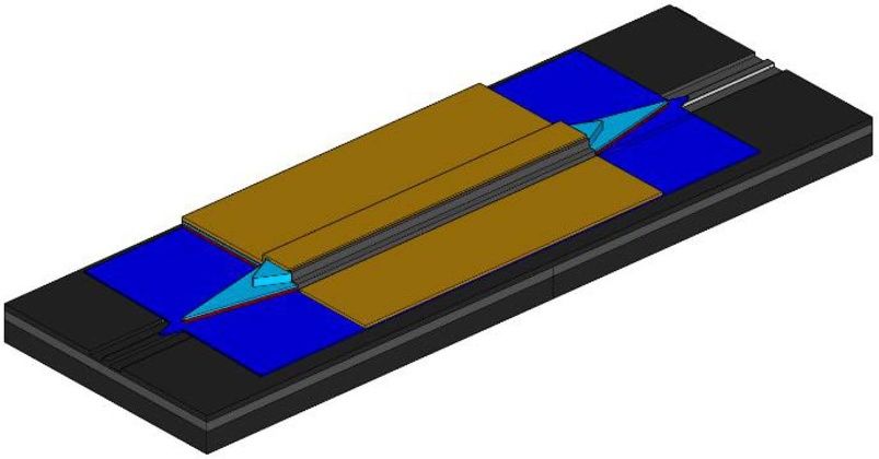
Figure 6. The measured spectrum of the hybrid silicon laser under
Gbit/s discretely tunable InP-on-silicon filtered feedback
50 mA driving current at room temperature. laser with sub-nanosecond wavelength switching times Opt.
Express 26 8059
[7] Fang A W, Park H, Cohen O, Jones R, Paniccia M J and
Bowers J E 2006 Electrically pumped hybrid
Figure 6 shows the lasing spectrum of the hybrid silicon AlGaInAs-silicon evanescent laser Opt. Express
laser driven at 24 mA. We have observed a lasing spectrum 14 9203–10
with a longitudinal mode, and the lasing wavelength is about [8] Fang A W, Lively E, Kuo Y-H, Liang D and Bowers J E 2008
1542.2 nm. A distributed feedback silicon evanescent laser Opt. Express
16 4413–9
[9] Zhang C, Srinivasan S, Tang Y, Heck M J R, Davenport M L
4. Conclusion and Bowers J E 2014 Low threshold and high speed short
cavity distributed feedback hybrid silicon lasers Opt.
Express 22 10202
In summary, a hybrid silicon evanescent laser with the SBG
[10] Shi Y et al 2014 High channel count and high precision
structure based on the REC technique is designed and fabric- channel spacing multi-wavelength laser array for future
ated by directly wafer bonding III–V wafer with SOI wafer. PICs Sci. Rep. 4 7377
The fabricated device’s lasing wavelength is 1542.2 nm, the [11] Shi Y, Li L, Zheng J, Zhang Y, Qiu B and Chen X 2014
threshold current is 24 mA, and the output power from sil- 16-wavelength DFB laser array with high channel-spacing
uniformity based on equivalent phase-shift technique IEEE
icon waveguide is up to 0.3 mW at room temperature under
Photon. J. 6 1502711
the continuous-wave operation. [12] Pintus P et al 2011 Low-loss hybrid silicon tapers IEEE Int.
Our next plan is to design and fabricate multi-wavelength Conf. Group IV Photonics pp 59–61
hybrid silicon laser arrays with 50 GHz/100 GHz wavelength [13] Arnaud L et al 2018 Fine pitch 3D interconnections with
spacing for silicon PICs in dense wavelength division multi- hybrid bonding technology: from process robustness to
reliability Proc. IEEE Int. Reliability Physics Symp.
plexing system.
pp 4D.4-1–7
[14] Ryohei H, Takashi S and Kazuhiro H 2018 GaN
microring waveguide resonators bonded to silicon
Acknowledgments substrate by a two-step polymer process Appl. Opt.
57 2073
This work is supported by the Chinese National Key Basic [15] Desomberg J, Fournel F, Moriceau H, Roule A, Barthel E and
Research Special Fund (2017YFA0206401), the Strategic Rieutord F 2018 Influence of water diffusion in deposited
silicon oxides on direct bonding of hydrophilic surfaces
Priority Research Program of the Chinese Academy of Microsyst. Technol. 24 801–8
Sciences (XDB24010100, XDB24010200, XDB24020100, [16] Bongyong J et al 2016 A hybrid silicon evanescent quantum
XDB24030100). dot laser Appl. Phys. Express 9 092102
4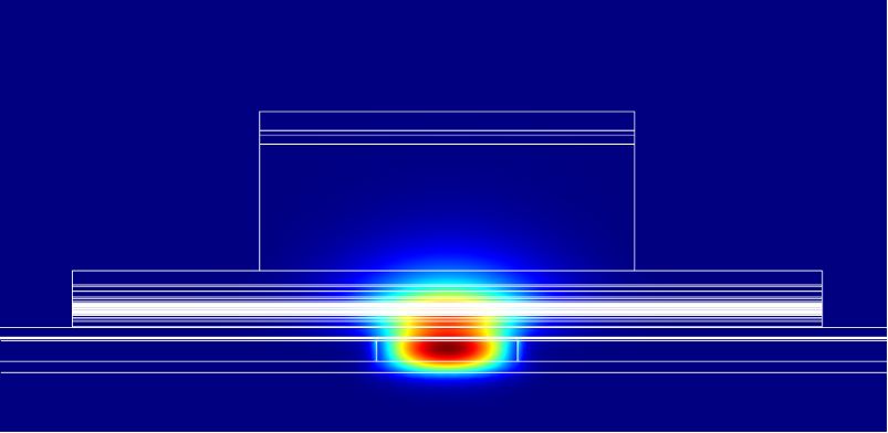
You can also read