A low-noise on-chip coherent microwave source - arXiv
←
→
Page content transcription
If your browser does not render page correctly, please read the page content below
A low-noise on-chip coherent microwave source
                                            Chengyu Yan1,2,* , Juha Hassel3,4 , Visa Vesterinen4 , Jinli Zhang1,5 , Joni Ikonen1 , Leif
                                            Grönberg4 , Jan Goetz1,3 , and Mikko Möttönen1,4,*
                                            1 QCD  Labs, QTF Centre of Excellence, Department of Applied Physics, Aalto University,P.O. Box 13500, FI-00076
                                            Aalto, Finland
                                            2 MOE Key Laboratory of Fundamental Physical Quantities Measurement & Hubei Key Laboratory of Gravitation

                                            and Quantum Physics, PGMF and School of Physics, Huazhong University of Science and Technology, Wuhan
                                            430074, P. R. China
                                            3 IQM, Keilaranta 19, 02150 Espoo, Finland
arXiv:2103.07617v2 [quant-ph] 23 Nov 2021

                                            4 QTF Centre of Excellence, VTT Technical Research Centre of Finland Ltd,P.O. Box 1000, FI-02044 VTT, Finland
                                            5 College of Electronic Information and Optical Engineering, Nankai University, Tianjin, 300071, China
                                            * corresponding author(s): Chengyu Yan(chengyu yan@hust.edu.cn), Mikko Möttönen(mikko.mottonen@aalto.fi)

                                            ABSTRACT

                                            The scaleup of quantum computers operating in the microwave domain requires advanced control electronics, and the use of
                                            integrated components that operate at the temperature of the quantum devices is potentially beneficial. However, such an
                                            approach requires ultra-low power dissipation and high signal quality in order to ensure quantum-coherent operations. Here,
                                            we report an on-chip device that is based on a Josephson junction coupled to a spiral resonator and is capable of coherent
                                            continuous-wave microwave emission. We show that characteristics of the device accurately follow a theory based on a
                                            perturbative treatment of the capacitively shunted Josephson junction as a gain element. The infidelity of typical quantum gate
                                            operations due to the phase noise of this cryogenic 25-pW microwave source is less than 0.1% up to 10-ms evolution times,
                                            which is below the infidelity caused by dephasing in state-of-the-art superconducting qubits. Together with future cryogenic
                                            amplitude and phase modulation techniques, our approach may lead to scalable cryogenic control systems for quantum
                                            processors.

                                                 Quantum computing has developed rapidly in the last decade using a range of different physical systems1–6 . For example,
                                            semiconductor and superconductor-based qubits with frequencies in the microwave regime have been studied extensively1, 2, 7, 8 .
                                            In such systems, the control of a large quantum processor is typically implemented by channelling a sequence of microwave
                                            pulses to the qubits operating at many different frequencies. This can be achieved using conventional room temperature
                                            electronics. However, the approach requires a large number of broad-band connections scaling linearly with the number
                                            of qubits, to transmit signals from room temperature to the refrigerator that hosts the quantum processor at temperatures
                                            typically below 100 mK. When scaling-up of these quantum-computing systems, the heavily attenuated bundles of coaxial
                                            microwave cables will determine much of the system-level requirements, including the cooling power and the physical size of
                                            the refrigerator9 . Cable lengths also lead to latencies and limitations in, for example, quantum error correction10, 11 .
                                                 Cryogenic integrated control electronics can potentially overcome these challenges. Independent of how the cryogenic
                                            control electronics are realised, any viable approach will need stable microwave sources integrated in the relevant operating
                                            environment to, for example, create the carrier frequencies for the modulated pulses12 . Josephson-junction-based sources have
                                            previously been studied in the field of radio astronomy as local oscillators for receivers in the millimetre and submillimetre
                                            wave bands13 . However, for typical solid-state quantum information processing applications operating in the sub-20-GHz
                                            band, the specific requirements are stringent. In particular, an on-chip microwave source should exhibit a very low power
                                            dissipation, long coherence time, and low noise. Some of these properties have previously been explored with prototype devices
                                            based on quantum dots14–16 and Josephson junctions17, 18 embedded in resonators. Similar designs can also find applications in
                                            generating non-classical radiation19, 20 . However, detailed design guidelines for specific applications are generally lacking and
                                            it remains unclear whether the signal quality of these systems will be sufficient for high-fidelity qubit operations.
                                                 In this Article, we report an on-chip coherent microwave source based on a Josephson junction strongly coupled to a
                                            spiral resonator. We develop a quantitative theoretical model for the resonator-coupled Josephson junction which operates in a
                                            particular parameter regime and can yield a stable and coherent continuous-wave microwave output. Our theory is verified
                                            in experiments which also provide relevant system parameters, including the output power and the microwave generation
                                            efficiency. We also confirm the applicability of our source for quantum-coherent operations by measuring the phase noise of
                                            the oscillator output, and provide the total phase noise spectrum up to large offset frequencies and evaluate its impact on the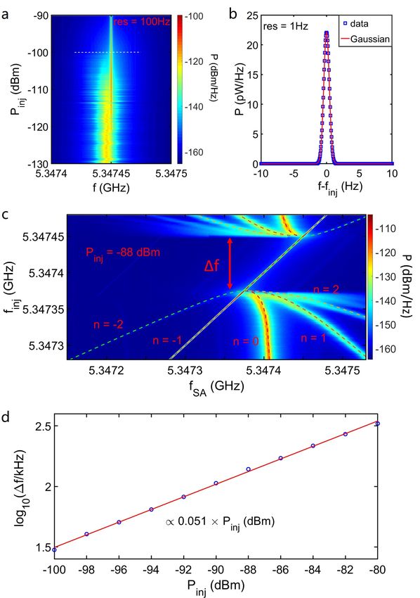
dephasing of an ideal qubit.
    We analyse, in particular, the source-induced infidelity of the identity operation and of the NOT gate for an ideal qubit,
and conclude that they lie below 0.1% up to a 10-ms evolution. We achieve this performance metric with a total cryogenic
power consumption of 200 pW—which is compatible with the millikelvin environment—and a generation efficiency of about
15%. We thus suggest that the source is compatible for driving qubits in schemes, in which it is combined with additional
amplitude and phase modulation components. Due to the high output power, our on-chip source may also be of potential
use in other applications, such as writing and retrieving quantum information encoded in spin ensembles21 and pumping a
microwave-to-optical photon converter22 .

Theory and design
Our oscillators are realized as capacitively shunted Josephson junctions (C-shunt JJs) coupled to a resonator. Under certain
conditions described below, the phase dynamics of a C-shunt JJ locks to a radiation field that couples to it23 . The phase-locked
and biased junction generates power at the corresponding angular frequency ω.
     Our devices reside in the parameter regime corresponding to relatively high Josephson coupling energies in the range of
EJ /h & 1 THz, where h is the Planck constant. Furthermore, it is known that the required harmonic phase-locking conditions are
favored in the case  24 ω  ω , i.e., the generated angular frequency ω sufficiently exceeds the plasma angular frequency of the
                 √              p
junction ωp = 8EJ Ec , where Ec is the charging energy of the junction. The plasma frequencies of bare junctions are typically
much higher than our frequency range of interest, 1–10 GHz, which motivates us to decrease ωp with a capacitive shunt. To this
end, we use an additional parallel-plate capacitor with the effective charging energy Ec = e2 /(2Cs ) ≈ h× 100–600 kHz, where
e is the elementary charge, or equivalently a shunt capacitance Cs in the range of 30–200 pF.
     The utilized harmonic modes in our devices are implemented in planar resonators, either as lumped LC resonators or spiral
resonators. In either case, the designed mode profile corresponds to that of the equivalent L1 –C1 series resonator as shown
in Fig. 1a, i.e., there is a current maximum at the junction. The dissipation, including coupling to the load, possible intrinsic
damping mechanisms, and the dissipation from the bias circuitry are formally included in the series resistance R1 . Note that the
parameters of the equivalent circuit can be extracted by standard circuit analysis from the device design parameters, and hence
can be considered known in the discussion below. Furthermore, we implement the voltage bias across the junction by applying
direct current (DC) through a shunt resistor Rs connected in parallel with the junction as shown in Fig. 1d. The detailed schemes
for implementing the bias and for the coupling of the output radiation are detailed in the Supplementary Information (SI).
     Our theoretical approach is based on a perturbative treatment of the C-shunt JJ under a radio-frequency (RF) drive, see
Methods section for the detailed derivation. Since ω  ωp , the voltage bias across the shunted junction is relatively accurately
given by the voltage across the shunt capacitor assuming that all the current drive is simply charging and discharging the
capacitor. Thus we define our unperturbed circuit to consist only of the shunt capacitor and the drive.
     In the next step, we treat the Josephson effect as a perturbation that slightly adjusts the current of the shunt capacitor and
hence the voltage, see Fig. 1b. The gain properties of this driven circuit composing of the junction and the shunt capacitor can
be extracted from the Fourier–Bessel expansion of the current-phase relation of a JJ assuming that the junction dynamics is
phase-locked to the first Shapiro step with the average voltage of hUi = Φ2π 0ω
                                                                                , where Φ0 = h/(2e). The solution is conveniently
represented in Fig. 1c by a complex impedance ZJ = RJ + XJ , in which RJ and XJ correspond to the real and imaginary
components as

               h̄ωhIJ i
      RJ = −                                                                                                                      (1)
                 eI12

                                           s                  !
             1     Ic                            hI i 2
                                                      J
      XJ =      1 − [J0 (ei1 ) − J2 (ei1 )] 1 −                                                                                   (2)
           iωCs    I1                            Ic J1 (ei1 )

where h̄ = h/(2π), hIJ i is the DC current through the junction, I1 is the current amplitude of the self-sustained oscillation
of the system at angular frequency ω, ei1 = Φ2πI  1
                                                ω 2C
                                                     , Ic is the critical current of the junction, and Jn refers to the nth-order
                                                  0   s
                                                                                                 Φ0 ω
Bessel function of the first kind. As detailed in the SI, hIJ i can be expressed as hIJ i = Ib − 2πR s
                                                                                                       , where Ib and Rs are the total
bias current and the resistance parallel to the junction at DC, respectively. The fact that RJ is negative for positive hIJ i is a
manifestation of the power generation ability23 .
    To provide intuitive understanding of the electrodynamics of the source, we note that the power output properties are related
to the real component of the impedance, RJ , whereas the imaginary component XJ slightly modifies the resonator frequency. In
a steady state, the photon emission rate from the JJ to the resonator equals that of the resonator decay, satisfied for RJ = −R1
according to Fig. 1c. Formally, we can express the total losses including the Josephson effect by RJ + R1 such that the total

                                                                                                                                 2/14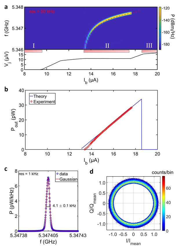
p
effective quality factor assumes the form Qtot = L1 /C1 /(RJ + R1 ), where we have for simplicity neglected to effect of XJ .
Thus the sustained oscillations corresponding to RJ = −R1 lead to a diverging Qtot . Due to the amplitude dependence of RJ ,
one obtains at each bias point a single well-defined amplitude for the sustained oscillation.
     The total RF power generation is given by Pout = −(Qt /Qe )RJ I12 /2 = (Qt /Qe )hIJ ih̄ω/(2e) where Qt and Qe are the
experimentally measurable total and loaded quality factors excluding the Josephson effect (see SI). The phase-locking condition
implies24 hIJ i < Ic |J1 (ĩ1 )|. Therefore, the maximum power available from the oscillator is Pout,max = 0.58 × Ic h̄ω/(2e) where
the numeric prefactor follows from the properties of Bessel functions, i.e., from maxx |J1 (x)| ≈ 0.58. Thus, an oscillator for a
desired power level and a given frequency may be optimized by choosing Ic accordingly. Technologically, the range of available
critical currents spans several orders of magnitude25 . Note that the maximum power output is obtained by optimizing the load
such that R1 ≈ 0.68 Φ πI     C
                          C2 ω 3
                                  and minimizing the residual microwave losses such that ηmw ≡ Qt /Qe ≈ 1 (see SI).
                      0 s
    To account for the imaginary component, we note that XJ yields a small correction to the reactance of the excited mode,
and results in a small shift in the output frequency. Its bias point dependence maps into the corresponding dependence for
the output frequency. This phenomenon is anticipated to affect the quality of the output signal, since a fluctuating bias point
thus leads to fluctuations in the frequency and hence in the phase of the output, as studied for different types of Josephson
oscillators in the literature26p
                               . The relative effect of XJ in the total reactance is minimized by maximizing the characteristic
impedance of the resonator L1 /C1 . This provides a guideline to resonator optimization in order to achieve higher frequency
and phase stability of the output signal: maximize the impedance under the constraints set by the resonator design. Although
we can achieve much higher resonator impedances given our design rules, we set here the impedance to roughly 100 Ω so that
the dependence between the emission frequency and the DC bias can be conveniently experimentally observed. This allows
us to demonstrate the validity of our model explicitly. Further improvement of the linewidth can be realized by increasing
the characteristic impedance of the resonator, which may be obtained by decreasing the metallization ratio of the distributed
transmission line resonator design and by using a thin film of high-kinetic-inductance material.

Experimental results
After the calibration of the gain of the amplification chain (Fig. S3), the microwave emission spectrum is measured and shown
in Fig. 2a as a function of the DC bias current Ib which is converted to the DC bias voltage by the on-chip shunt resistor. We
observe three bias regions with distinctive signatures in both the current-voltage (IV) characteristics and the emission spectrum
as follows: the supercurrent state for Ib < 10 µA (region I), the self-induced Shapiro step23, 27 for 13 µA < Ib < 18 µA (region
II), and the normal state with the resistance determined by the shunt resistor for Ib > 19 µA (region III). There is no photon
emission in region I and negligible emission in region III. In the contrast, a major emission occurs at the Shapiro step in region
II. The Shapiro step is a manifestation of the self-induced locking of the Josephson and resonator dynamics leading to the
measurable power emission. The central frequency of the emitted signal shifts towards higher frequency with increasing Ib
owing to above-mentioned XJ [Fig. 2a]. This behaviour is well captured by our model.
     The emitted power, shown in Fig. 2b, is obtained by integrating the emission spectrum over frequency. The power increases
almost linearly with increasing Ib , again well captured by the model. The output power exceeds 20 pW for Ib > 16 µA peaking
at 28 pW (−75.5 dBm) with a corresponding DC power PDC = 17.7 µA × 10.7 µV = 189 pW (−67.2 dBm). This suggests a
DC-to-RF conversion efficiency of 15% at maximum output power. As shown in Fig. 2c, the typical emission linewidth is
4.1 ± 0.1 kHz which is roughly five times as sharp as that obtained in ref.18 (∼22 kHz). Such a narrow linewidth suggests
potential for a noticeable improvement of phase stability over previous coherent cryogenic sources14–18, 28, 29 .
     Interestingly, we use only a single-pole room temperature commercial low-pass filter on the DC line in the present setup,
whereas filters at multiple temperature stages have been utilized in previous studies18 . Thus our filtering scheme relaxes some
of the burden required to build and test the experimental setup. However, improvements on the filtering scheme in our setup
may lead to further narrowing of the spectral line.
     To find evidence that the output of our source is composed of microwaves in a coherent state, we utilize the heterodyne
detection technique. The output field is demodulated by a local reference tone to yield the in-phase (I) and quadrature-phase
(Q) components. The frequency of the reference tone is detuned from the central emission frequency by 62.5 MHz, optimized
for our setup. The results of 106 samples are summarized as a two-dimensional (2D) probability distribution depicted in Fig. 2d.
The probability distribution of the output shows a nearly Gaussian shape with respect to the intensity of the radiation field, or
the radius in Fig. 2d, as detailed in Fig. S7. The Gaussian ensembles rotates at an intermediate frequency of 62.5 MHz in the IQ
plane, and hence resembles a ring with finite radius and width. This coincides with the distribution of a coherent state averaged
over different phase shifts, hence our observation provides evidence on the coherent character of the emission.
     In Fig. S8, we provide data on a reference device differing from that discussed here mainly in its lower critical current,
roughly 1.8 µA, and having a lumped-element LC resonator. In addition, the resonator impedance is ∼ 3.8 Ω as opposed to
∼ 75 Ω for the spiral resonator. As expected from the discussion above, the frequency of the emitted signal in Fig. S8 is
much more sensitive to the bias current than for the spiral-resonator sample. Thus the emitted signal is expected to experience

                                                                                                                             3/14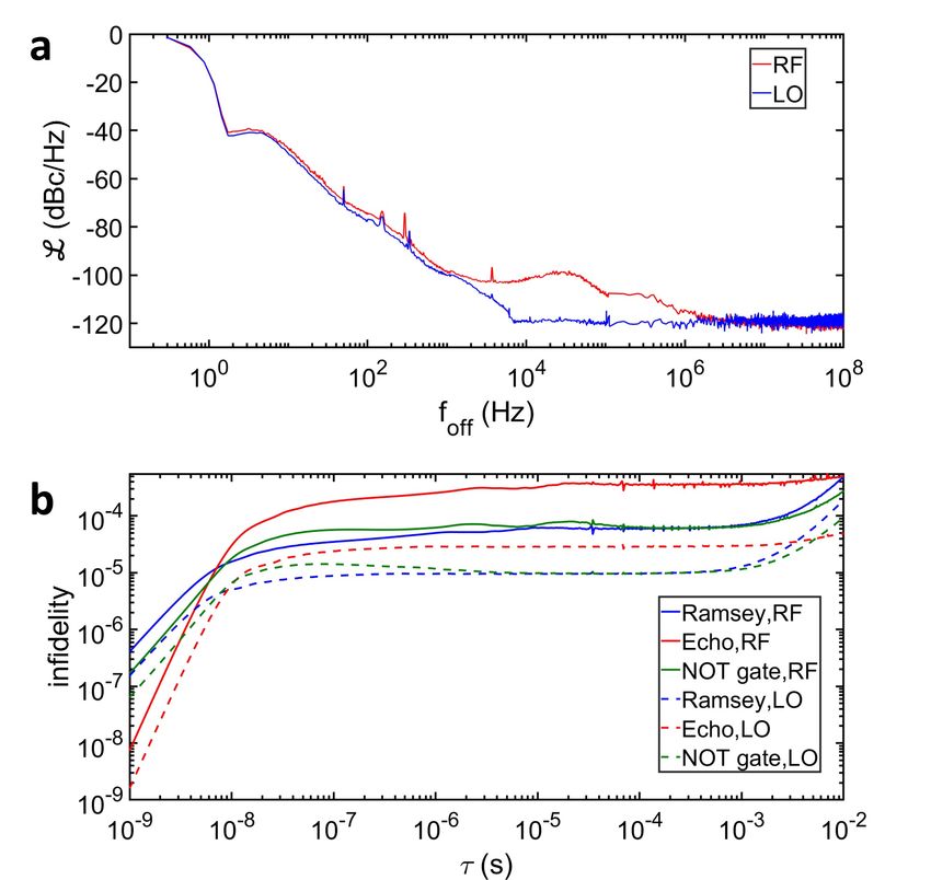
excessive phase noise. Nevertheless, the good agreement of the experimental data with our theory for this sample of very
different parameters than those of the spiral-resonator sample provides a convenient verification of our model.
     To gain more understanding on possible limitations of the linewidth of the generated signal, we utilize the well-established
injection locking technique14, 15, 18, 30 . Here, the frequency of the injection tone finj is fixed to that of the free emission at a
given bias, whereas the power Pinj is swept.
     Figure 3a illustrates that in our experiments, the injection tone induces a very sharp peak into the emission spectrum, into
which the whole emission gradually shifts with increasing injection power. For Pinj > −100 dBm, we observe only a single
emission peak with a linewidth of 1 Hz (Fig 3b). Interestingly, this linewidth is limited by the smallest resolution bandwidth of
the used spectrum analyzer and our more detailed study of the measured spectrum shown in Fig. S12 suggests that the linewidth
of the injection-locked source is of the order of 1 mHz or below. It is also possible to measure very small linewidths with an
advanced hardware setup, for example, by carrying out a Fourier transform of the IQ traces after sufficient averaging. Yet, we
note that, the typical linewidths of state-of-the-art superconducting qubits are in the kilohertz range, i.e., comparable to the
linewidth of our source without injection locking, see Fig. 2c. We have also measured the emission spectrum with a fixed Pinj
but varying finj , and the results agree well with Adler theory, as shown in Figs. 3c and d, and discussed in the SI.
     We extract the the phase noise L from the emission spectrum under injection locking with Pinj = −100 dBm where the
injection tone contributes less than 1% of the total power. Our results presented in Fig. 4a show that L decays rapidly with
increasing frequency offset foff from finj . It reaches −95 dBc/Hz at foff = 10 kHz, which is about 15 dB below the corresponding
value for a typical lab-grade local oscillator (LO) operating at room temperature12 , but it needs further improvement to be
compatible with high-precision LOs such as that used to generate the injection tone. The measured phase noise eventually
saturates to −120 dBc/Hz at ∼5 MHz. The saturation is mainly determined by noise added by our amplification chain (Fig. S10).
The noise floor can be possibly subtracted to a large extent from the source noise by averaging the data carefully for the offset
frequency exceeding 5 MHz (Fig. 4).
     It is possible to minimize the influence of the system noise using the cross-correlation technique31 and thus to obtain the
actual L at large foff . We leave this extension for future research. Nevertheless, we note that L = −116 dBc/Hz at an offset
frequency of 1 MHz is well below −99 dBc/Hz obtained by the quantum-dot-based on-chip microwave source studied in ref.15 .
     Owing to the large output power and hence the large signal-to-noise ratio, the phase noise L yields the dominating noise of
the device up to relatively large offset frequencies. This motivates us to examine the influence of the phase noise on apparent
qubit dephasing and on the gate and operation fidelity. We consider the source, augmented with a noiseless pulse and phase
modulator, to drive an ideal qubit that is free of intrinsic dephasing and dissipation. Following the framework of ref.12 , we
calculate the infidelity of the quantum operations, defined as 1 − Fav (τ), where the averaged operational fidelity is denoted by
Fav (τ). We have
                                                                 1
                                                        Fav (τ) ≈ [1 + e−X(τ) ]
                                                                 2
where the evolution time is denoted by τ,
                                             1                                      1
                                                  Z ∞
                                     X(τ) =             d f 10L ( f )/(10 dBc/Hz)        ∑ Gz,l ( f , τ)
                                            2π     0                                Hz l∈x,y,z

and Gz,l ( f , τ) is a filter function that quantifies the action of the control Hamiltonian and hence depends on the specific quantum
operation as discussed in the SI.
     Figure 4b shows the calculated infidelity for prototypical quantum operations: Ramsey, Hahn echo, and NOT gate operations.
The infidelity is ∼ 0.1% for all these operations after a long evolution time of τ = 10 ms. These infidelities are an order of
magnitude lower than those achieved by a typical lab-grade LO12 . However, in the short τ limit, the calculated infidelity is
about an order of magnitude larger than that obtained from lab-grade LO12 due to the overestimated phase noise L at large
foff arising from the amplification chain. The low-offset-frequency components dominate in the long τ limit. On the other
hand, both low- and high-frequency components have a noticeable contribution in the short τ limit as discussed in the SI.
For comparison, the infidelities of the operations are reduced by an order of magnitude if extract them from the phase noise
measured for the LO. These infidelities are also significantly affected by the noise floor set by the amplification chain. Same
calculation with the noise floor subtracted can be found in the SI.
     The above-measured low noise of our microwave source suggests that the device is suitable for controlling state-of-the-art
superconducting qubits with coherence times currently reaching 100 µs32–34 .

                                                                                                                                4/14
Conclusions
In this work, we demonstrated an on-chip coherent microwave source realized by a Josephson junction strongly coupled to
a spiral resonator. The source can generate microwave signals with narrow linewidth (< 1 Hz, suggestively . 1 mHz), low
noise (< −120 dBc/Hz), high output power (> 25 pW), and a fine dc-to-rf power conversion efficiency of about 15%. The
output power is two orders of magnitude higher than that previously reported for double-quantum-dot sources14–16 or an
aluminum-junction source18 . We confirm that the expected infidelity bound arising from the phase noise of our source in a
typical quantum-logic operation is below 0.1% up to 10-ms evolution ensuring that the signal quality is sufficient for the control
of state-of-the-art quantum systems.
We used the injection-locking technique in an effort to study the intrinsic limitations of the oscillator. As for any oscillating
source independent of the technology, frequency and phase stabilization techniques need to be used. An alternative to this
injection locking scheme is to bring the reference tone to the cryogenic temperature at a low-frequency band restricting the
bandwidth requirements from room temperature, and to use frequency multiplication techniques35 to generate the injection tone.
Furthermore, integration of superconducting quantum interference devices (SQUIDs) with the source allows to tune the emission
frequency without significant amplitude modulation, and hence enables frequency stabilization based on phase-locked loops
which are typically used in the context of voltage-controlled oscillators at room temperature, and for which superconducting
counterparts have been demonstrated as well13 .
In general, there are several approaches pursued in the field of integrated control of quantum systems, including cryogenic
semiconductor-based techniques, or even those based on optical-to-microwave transducers22 . Semiconductor-based oscillators
have been demonstrated with the output power of about 0.2 µW at 1.5 K36 . Full semiconductor-based cryogenic control systems
have been demonstrated at the operating temperatures of a few kelvin, with power consumption of the order of 100 mW37 .
Cryogenic semiconducting electronics has been demonstrated at the tempearture of 100 mK, with power consumption of
18 nW per cell38 . While less matured, all-superconducting control electronics concepts are likely superior in power efficiency.
Ideally, the power dissipated at the base temperature is efficiently converted into the control signals of the quantum system. An
order-of-magnitude estimate for our source, assuming a 100-ns-long control period or readout pulses of 10 photons at 5.3 GHz
enables driving about 7000 qubits with the output power available.
The power and signal quality alone does not yet guarantee the source to be useful in the control of quantum systems. A
feasible scheme for millikelvin-operated full waveform control may be a combination of our source with cryogenic microwave
phase shifters39, 40 or flux-tunable resonators41 and quantum-circuit refrigerators42, 43 , enabling power-efficient waveform
control. Moreover, cryogenic mixing or parametric frequency conversion techniques are an option for full waveform generation.
Importantly, we anticipate that a stable microwave source is useful in other contexts than direct qubit control such as those
based on single-flux-quantum (SFQ) logic44 needing a master clock reference. Compared to semiconductor counterparts,
SFQ is orders of magnitude more power efficient45 . In general, it is understood that the field of integrated control systems
in cryogenic solid-state quantum technology is still at its infancy. Independent of the detailed realization, it is expected that
a power-efficient low-phase-noise reference oscillator is a necessary component, acting as the primary source of microwave
power and as reference master clock.
In the future, we aim to study the properties of cascaded cryogenic sources, where one injection-locked source works as the
locking tone for other sources. In such a scenario, the total injection power delivered from room temperature, and hence the
required amount of microwave cables, is independent of size of the cryogenic control system such as the number of qubits in a
large-scale quantum computer.
Furthermore, we aim to study the thermalization of the output impedance of the source. Although the measured phase noise
also includes the effect of finite temperature, thermal photons leaking to different parts of a quantum computer may lead to
additional undesired dephasing. Fortunately, our preliminary thermal analysis and that in ref.46 suggests that the shunt resistor
can be thermalized well below 100 mK even at high output powers. In fact, a cryogenic source may also be able to utilize
the exponential thermal suppression of noise photons at the signal frequency, in stark contrast to signals generated at room
temperature, after which the suppression of noise photons by cryogenic attenuation or filtering leads to equal suppression of the
signal power.
5/14Methods
Theoretical model. Let us develop an analytic model for the Josephson oscillators based on a capacitively shunted Josephson
junction coupled in parallel with a resonator circuit. The concept is to first derive an analytic model for the junction as a gain
element. Then the gain properties are analyzed for the resonator-coupled junction. The mathematical tools used include (i)
well-known conditions of junction phase-locking to an RF drive, (ii) a perturbative harmonic analysis of the junction to provide
the gain properties under the RF drive and the phase-locking conditions, and (iii) showing by a power-balance criterion that
the gain and phase-locking conditions satisfy a stable sustained oscillating mode by the self-generated RF drive. For (ii), the
junction properties are described as an effective impedance, the negative real part of which is the manifestation of the gain. The
model provides a convenient engineering tool for obtaining the basic properties of the oscillator. Namely, it provides simple
design criteria for stable oscillator operation that can be used to predict the output power, DC-to-RF conversion efficiency, and
curiously, the operation-point-dependent output frequency.
We begin our analysis from an RF-driven capacitively shunted Josephson junction, as shown in Fig 1. In the first step, let us
consider a bare capacitively shunted √ Josephson junction. Assume that the junction is subjected to an RF current IRF = I1 sin(ωt)
such that ω
ωp , where ωp = 1/ LJCs , is the junction plasma frequency, LJ is the Josephson inductance, and Cs is the
capacitance parallel to the junction. The capacitance Cs is dominated by the shunt capacitance since the intrinsic capacitance of
the junction is negligible. Under the above assumptions, the RF drive couples predominantly capacitively through the parallel
connection of the junction and the shunt capacitance. Thus, the unperturbed voltage, neglecting the Josephson effect, across the
tunnel junction is simply
1 I1
Z
VT (t) = I1 sin(ωt)dt = − cos(ωt) + hUi (3)
Cs ωCs
where the constant of integration is the DC voltage across the junction.
We employ the AC Josephson relation to obtain the phase across the junction as
2π 2πI1 2π
Z
φ= VT dt = − sin(ωt) + hUit − φc (4)
Φ0 Φ0 ω 2Cs Φ0
where we have defined the constant of integration −φc . Next, we utilize the Josephson current-phase relation IJ = Ic sin φ which
provides the current through the Josephson tunnel element as
IJ = Ic sin[−ei1 sin(ωt) + ωt − φc ] (5)
where we have defined ei1 = Φ2πI 2
1
and written hUi = Φ0 ω/(2π) by adopting the phase-locking condition, i.e., the system
0 ω Cs
is biased on the first Shapiro step. This condition is analyzed in the SI to check the validity range of the solutions. Here, we
merely assume it. We rewrite equation (5) with the help of its Fourier–Bessel series as
∞
IJ (I0 , I1 , t) = Ic ∑ Jm (ei1 ) sin[ωt(1 − m) − φc ] (6)
m=−∞
Let us first consider the direct current hIJ i through the tunnel element. In equation (6) this follows from the term m = 1 as
hIJ i = Ic J1 (ei1 ) sin(−φc ) (7)
Φ0 ω
In fact, hIJ i = Ib − 2πR s
is related to external direct bias current (see SI) Ib . Solving for φc yields
hIJ i
φc = arcsin − (8)
Ic J1 (ei1 )
To address the RF properties, we consider the fundamental-frequency component of IJ (t) which follows from equation (6),
picking terms m = 0 and m = 2 as
IJ1 (t) = Ic [J0 (ei1 ) sin(ωt − φc ) + J2 (ei1 ) sin(−ωt − φc )] (9)
Using a Bessel recurrence formula and equation (8), leads to
s
hI i 2 2hIJ i
J
IJ1 (t) = Ic [J0 (ei1 ) − J2 (ei1 )] 1 − sin(ωt) + J1 (ei1 ) cos(ωt) (10)
Ic J1 (i1 )
e i1 J1 (ei1 )
e
6/14In the capacitively shunted junction case, the RF current IJ1 couples back to the shunt capacitance since we assume that it is
the dominant impedance at frequency ω. As this happens, a voltage emerges on top of VT of equation (3). Marking this voltage
perturbation as VP (t) we obtain
s
Ic hI i 2 2hIJ i
J
VP (t) = [J0 (ei1 ) − J2 (ei1 )] 1 − cos(ωt) − sin(ωt) (11)
ωCs Ic J1 (i1 )
e i1 ωCs
e
Let us convert equations (3) and (11) into frequency plane by identifying the in-phase sin(ωt) and quadrature cos(ωt)
components to write Vetot (ω) = VeT (ω) + VeP (ω). Furthermore, it is practical to write the output in the form of impedance
ZJ (ω) = Vetot (ω)/I1 . From equations (3) and (11) and by arranging the quadratures, it follows
s
2hIJ i 1 Ic hI i 2
J
ZJ (ω) = − −i +i [J0 (ei1 ) − J2 (ei1 )] 1 − (12)
ei1 I1 ωCs ωCs ωCs I1 Ic J1 (ei1 )
2πI1
Insertion of the definition ei1 = Φ0 ω 2Cs
here yields
( s )
ωΦ0 hIJ i 1 Ic hI i 2
J
ZJ (ω) = − + 1 − [J0 (ei1 ) − J2 (ei1 )] 1 − (13)
πI12 iωCs I1 Ic J1 (ei1 )
We stress that the real part of the junction impedance is negative if hIJ i > 0, and hence represents gain. Note that here the
direction of positive current is fixed by the choice that we operate at the first positive-voltage Shapiro step. The imaginary
part of the junction impedance equals to that of the shunt capacitor modified by a nontrivial perturbative term due to the
Josephson effect. Equation (13) yields equations (1) and (2) for the real and the imaginary component of the junction impedance,
respectively.
Device fabrication. The devices are fabricated in a multi-layer process for superconducting circuits, the key element of
which is a sidewall-passivated-spacer (SWAPS) technique25 for the Nb-Al/AlOx -Nb Josephson junctions. Figures 1b and S1
summarize the structure of the device. The fabrication begins with a hydrofluoric-acid (HF) dip of a 150-mm high-resistivity
silicon wafer to remove oxides from the surface. The trilayer stack for the junctions with thicknesses 100 nm/10 nm/100 nm
is then deposited, with a target critical-current density of 100 A/cm2 . We deposit the subsequent layers as follows: a second
120-nm-thick niobium layer, an atomic-layer-deposited 50-nm AlOx insulator for a parallel-plate capacitance density of roughly
1.5 fF/µm2 , a third niobium layer of 120-nm thickness, and a normal-metal layer with thickness of about 100–130 nm for a
sheet resistance of approximately 4 Ω/. The patterning of the layers is enabled by ultraviolet (UV) photolithography. The
niobium layers are etched with plasma, whereas the insulators and the resistors are wet etched. The Josephson oscillators are
fabricated in the same batch of wafers as the traveling-wave parametric amplifiers of ref.47 .
References
1. Houck, A. A. et al. Controlling the spontaneous emission of a superconducting transmon qubit. Phys. Rev. Lett. 101,
080502, DOI: 10.1103/PhysRevLett.101.080502 (2008).
2. Shinkai, G., Hayashi, T., Ota, T. & Fujisawa, T. Correlated coherent oscillations in coupled semiconductor charge qubits.
Phys. Rev. Lett. 103, 056802, DOI: 10.1103/PhysRevLett.103.056802 (2009).
3. Muhonen, J. T. et al. Storing quantum information for 30 seconds in a nanoelectronic device. Nat. Nanotechnol. 9, 986
(2014).
4. Neill, C. et al. A blueprint for demonstrating quantum supremacy with superconducting qubits. Science 360, 195–199
(2018).
5. Saffman, M. Quantum computing with neutral atoms. Natl. Sci. Rev. 6, 24–25, DOI: 10.1093/nsr/nwy088 (2018).
6. Arute, F. et al. Quantum supremacy using a programmable superconducting processor. Nature 574, 505–510 (2019).
7. Nadj-Perge, S., Frolov, S., Bakkers, E. & Kouwenhoven, L. P. Spin–orbit qubit in a semiconductor nanowire. Nature 468,
1084–1087 (2010).
8. Ristè, D. et al. Millisecond charge-parity fluctuations and induced decoherence in a superconducting transmon qubit. Nat.
Commun. 4, 1–6 (2013).
7/149. Krinner, S. et al. Engineering cryogenic setups for 100-qubit scale superconducting circuit systems. EPJ Quantum Technol.
6, 2, DOI: 10.1140/epjqt/s40507-019-0072-0 (2019).
10. Knill, E. & Laflamme, R. Theory of quantum error-correcting codes. Phys. Rev. A 55, 900–911, DOI: 10.1103/PhysRevA.
55.900 (1997).
11. Calderbank, A. R. & Shor, P. W. Good quantum error-correcting codes exist. Phys. Rev. A 54, 1098–1105, DOI:
10.1103/PhysRevA.54.1098 (1996).
12. Ball, H., Oliver, W. D. & Biercuk, M. J. The role of master clock stability in quantum information processing. npj Quantum
Inf. 2, 1–8 (2016).
13. Koshelets, V. et al. Towards a phase-locked superconducting integrated receiver: prospects and limitations. Phys. C:
Supercond. 367, 249 – 255, DOI: https://doi.org/10.1016/S0921-4534(01)01046-2 (2002).
14. Liu, Y.-Y., Stehlik, J., Gullans, M. J., Taylor, J. M. & Petta, J. R. Injection locking of a semiconductor double-quantum-dot
micromaser. Phys. Rev. A 92, 053802, DOI: 10.1103/PhysRevA.92.053802 (2015).
15. Liu, Y.-Y., Hartke, T. R., Stehlik, J. & Petta, J. R. Phase locking of a semiconductor double-quantum-dot single-atom
maser. Phys. Rev. A 96, 053816, DOI: 10.1103/PhysRevA.96.053816 (2017).
16. Liu, Y.-Y. et al. Threshold dynamics of a semiconductor single atom maser. Phys. Rev. Lett. 119, 097702, DOI:
10.1103/PhysRevLett.119.097702 (2017).
17. Chen, F. et al. Realization of a single-Cooper-pair Josephson laser. Phys. Rev. B 90, 020506, DOI: 10.1103/PhysRevB.90.
020506 (2014).
18. Cassidy, M. et al. Demonstration of an ac Josephson junction laser. Science 355, 939–942 (2017).
19. Grimm, A. et al. Bright on-demand source of antibunched microwave photons based on inelastic Cooper pair tunneling.
Phys. Rev. X 9, 021016, DOI: 10.1103/PhysRevX.9.021016 (2019).
20. Rolland, C. et al. Antibunched photons emitted by a dc-biased Josephson junction. Phys. Rev. Lett. 122, 186804, DOI:
10.1103/PhysRevLett.122.186804 (2019).
21. Grezes, C. et al. Multimode storage and retrieval of microwave fields in a spin ensemble. Phys. Rev. X 4, 021049, DOI:
10.1103/PhysRevX.4.021049 (2014).
22. Arnold, G. et al. Converting microwave and telecom photons with a silicon photonic nanomechanical interface. Nat.
Commun. 11, 4460 (2020).
23. Hassel, J., Grönberg, L., Helistö, P. & Seppä, H. Self-synchronization in distributed Josephson junction arrays studied
using harmonic analysis and power balance. Appl. Phys. Lett. 89, 072503, DOI: 10.1063/1.2337536 (2006).
24. Kautz, R. L. The ac Josephson effect in hysteretic junctions: Range and stability of phase lock. J. Appl. Phys. 52,
3528–3541, DOI: 10.1063/1.329132 (1981).
25. Grönberg, L. et al. Side-wall spacer passivated sub-µm Josephson junction fabrication process. Supercond. Sci. Technol.
30, 125016, DOI: 10.1088/1361-6668/aa9411 (2017).
26. Salerno, M., Samuelsen, M. R. & Yulin, A. V. Spectral linewidths of Josephson oscillators. Phys. Rev. Lett. 86, 5397–5400,
DOI: 10.1103/PhysRevLett.86.5397 (2001).
27. Barbara, P., Cawthorne, A. B., Shitov, S. V. & Lobb, C. J. Stimulated emission and amplification in Josephson junction
arrays. Phys. Rev. Lett. 82, 1963–1966, DOI: 10.1103/PhysRevLett.82.1963 (1999).
28. Langenberg, D. N., Scalapino, D. J., Taylor, B. N. & Eck, R. E. Investigation of microwave radiation emitted by Josephson
junctions. Phys. Rev. Lett. 15, 294–297, DOI: 10.1103/PhysRevLett.15.294 (1965).
29. Astafiev, O. et al. Single artificial-atom lasing. Nature 449, 588–590 (2007).
30. Marković, D., Pillet, J., Flurin, E., Roch, N. & Huard, B. Injection locking and parametric locking in a superconducting
circuit. Phys. Rev. Appl. 12, 024034, DOI: 10.1103/PhysRevApplied.12.024034 (2019).
31. Walls, W. F. Cross-correlation phase noise measurements. In Proceedings of the 1992 IEEE Frequency Control Symposium,
257–261 (1992).
32. Rigetti, C. et al. Superconducting qubit in a waveguide cavity with a coherence time approaching 0.1 ms. Phys. Rev. B 86,
100506, DOI: 10.1103/PhysRevB.86.100506 (2012).
33. Rol, M. A. et al. Fast, high-fidelity conditional-phase gate exploiting leakage interference in weakly anharmonic
superconducting qubits. Phys. Rev. Lett. 123, 120502, DOI: 10.1103/PhysRevLett.123.120502 (2019).
8/1434. Xu, Y. et al. Experimental implementation of universal nonadiabatic geometric quantum gates in a superconducting circuit.
Phys. Rev. Lett. 124, 230503, DOI: 10.1103/PhysRevLett.124.230503 (2020).
35. Rashid, H. et al. Frequency multiplier based on distributed superconducting tunnel junctions: Theory, design, and
characterization. IEEE Transactions on Terahertz Sci. Technol. 6, 724–736, DOI: 10.1109/TTHZ.2016.2583201 (2016).
36. Matheoud, A. V., Sahin Solmaz, N. & Boero, G. A low-power microwave HEMT LC oscillator operating down to 1.4 K.
IEEE Transactions on Microw. Theory Tech. 67, 2782–2792, DOI: 10.1109/TMTT.2019.2916552 (2019).
37. Patra, B. et al. A scalable Cryo-CMOS 2-to-20Ghz digitally intensive controller for 4×32 frequency multiplexed spin
qubits/transmons in 22nm FinFET technology for quantum computers. In 2020 IEEE International Solid- State Circuits
Conference - (ISSCC), 304–306, DOI: 10.1109/ISSCC19947.2020.9063109 (2020).
38. Pauka, S. et al. A cryogenic interface for controlling many qubits. Nat. Electron. 4, 64–70, DOI: https://doi.org/10.1038/
s41928-020-00528-y (2021).
39. Kokkoniemi, R. et al. Flux-tunable phase shifter for microwaves. Sci. Reports 7, 1–6 (2017).
40. Zhang, J. et al. Broadband tunable phase shifter for microwaves. AIP Adv. 10, 065128, DOI: 10.1063/5.0006499 (2020).
41. Osborn, K., Strong, J., Sirois, A. J. & Simmonds, R. W. Frequency-tunable Josephson junction resonator for quantum
computing. IEEE transactions on applied superconductivity 17, 166–168 (2007).
42. Tan, K. Y. et al. Quantum-circuit refrigerator. Nat. Commun. 8, 1–8 (2017).
43. Silveri, M. et al. Broadband Lamb shift in an engineered quantum system. Nat. Phys. 15, 533–537 (2019).
44. Li, K., McDermott, R. & Vavilov, M. G. Hardware-efficient qubit control with single-flux-quantum pulse sequences. Phys.
Rev. Appl. 12, 014044, DOI: 10.1103/PhysRevApplied.12.014044 (2019).
45. Savin, A. M. et al. High-resolution superconducting single-flux quantum comparator for sub-Kelvin temperatures. Appl.
Phys. Lett. 89, 133505, DOI: 10.1063/1.2357858 (2006).
46. Yeh, J.-H. et al. Hot electron heatsinks for microwave attenuators below 100 mK. Appl. Phys. Lett. 114, 152602, DOI:
10.1063/1.5097369 (2019). https://doi.org/10.1063/1.5097369.
47. Simbierowicz, S. et al. Characterizing cryogenic amplifiers with a matched temperature-variable noise source. Rev. Sci.
Instruments 92, 034708, DOI: 10.1063/5.0028951 (2021).
48. Hollmann, A. et al. 30 Ghz-voltage controlled oscillator operating at 4 K. Rev. Sci. Instruments 89, 114701, DOI:
10.1063/1.5038258 (2018).
Acknowledgements
We have received funding from the Centre for Quantum Engineering at Aalto under Grant number JVSG; European Research
Council under Grant No 681311 (QUESS) and MarieSkłodowska-Curie Grant No. 795159; Academy of Finland through its
Centres of Excellence Programme (project numbers 312300, 312059 and 312295) and grants (numbers 314447, 314448,
314449, 305237, 316551, 308161, 335460, and 314302). We thank Hannu Sipola, Roope Kokkoniemi, Jean-Philippe Girard,
and Jukka Pekola for useful discussion.
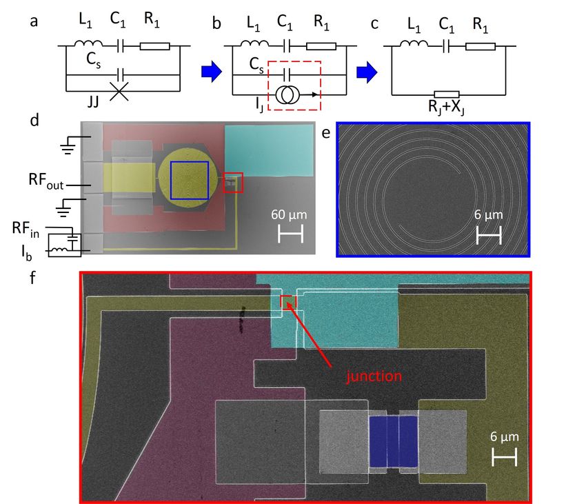
9/14Figure 1. Working principle and structure of the device. a, Simplified circuit diagram of the sample where L1 and C1 are
the equivalent inductance and capacitance of the microwave resonator, respectively, R1 models the losses of the resonator, and
Cs is the shunt capacitor in parallel with the Josepshon junction (JJ). b, In our perturbative treatment (see Methods for
mathematical derivation), we fist solve the voltage arising from the microwave current oscillations accounting only for the shunt
capacitor and then take into account how this voltage across the Josephson junction, behaving as a current source, perturbs the
current of the shunt capacitor. c, Resulting impact of the capacitively shunted JJ (red dashed box in (a)) on the resonator circuit
can be represented by an impedance RJ + XJ . A detailed circuit diagram can be found in Fig. S3. d–f, Overview of the device,
consisting of a Josephson junction coupled to a spiral resonator. The ground plane is denoted by pink color. The bias line and
the spiral resonator is highlighted in yellow. The shunt capacitor appears in cyan color. The area enclosed by the blue rectangle
in (d), is magnified in (e). The red rectangle in (d) denotes the area shown in (f). The junction has a size of ∼10 µm2 . The
∼1-Ω shunt resistor (blue color), with small inductance, functions as an on-chip current to voltage converter for the DC bias. A
schematic for the layered structure, which highlights the connections between the different layers, can be found in Fig. S1. The
nominal parameters of the device are designed as follows: the critical current Ic = 10 µA, the shunt capacitance Cs = 192 pF,
and the effective inductance and capacitance of the resonator are L1 = 2.0 nH and C1 = 0.36 pF, respectively.
10/14Figure 2. Characteristics of the spiral-resonator source. a, Top panel shows the calibrated power spectral density emitted
from the source as a function of the bias current and emission frequency. The red dashed trace indicates the position of the
emission peak predicted by equation (13), where we use only a single adjustable parameter that accounts for the parasitic
inductance mainly arising from the bonding wires. The bottom panel shows the direct-current voltage measured across the
junction as a function of the bias current. Labels I, II, and III refer to the supercurrent, Shapiro step, and normal-state bias
regions, respectively. Results from an extended range can be found in Fig. S5. b, Measured (red dots) and predicted (blue trace)
output power as a function of bias current. c, Line trace of (a) at Ib = 16.5 µA (markers) together with a Gaussian fit (solid line).
In all figures, ’res’ refers to the resolution bandwidth of the spectrum analyzer. d, Measured probability distribution of the
source output in the in-phase–quadrature (IQ) plane at Ib = 16.5 µA. The data is without digital down-conversion. Here, 106
samples are encoded into 200×200 bins. The obtained ring shape agrees with the coherent nature of the emitted signal. The
measurement was carried out at the base temperature of the fridge, ∼15 mK. The detailed experiment setup and probability
distribution after digital down-conversion can be found in the SI.
11/14Figure 3. Emission spectrum with injection locking. a, Power spectral density of the source emission as a function of
injection power Pinj at the sample. The frequency of the injection tone is fixed at 5.34745 GHz. b, Trace of (a) at Pinj = −100
dBm (markers) and a Gaussian fit (solid line). Here, the injection tone contributes less than 1% of the total power. The
linewidth of output signal is bounded from below by the minimum resolution of the spectrum analyzer to 1 Hz, which is also
responsible for the Gaussian shape. See Fig. S12 for a more detailed analysis of this data suggesting a linewidth for the output
of the source to be of the order of 1 mHz or below. c, Measured power spectral density with respect to the output of the source
as a function of the spectral frequency fSA and of the injection frequency finj at a fixed injection power of -88 dBm. ∆ f is
defined as the width of the frequency range where the emission signal is phase locked to the injection tone. Here Pinj = −88 is
chosen to highlight bending of peaks under injection locking condition. Similar plots at other injection power can be found in
SI. d, The frequency range ∆ f as a function of the injection power Pinj . The measured data (blue circles) are in good agreement
with the Adler theory (solid line). Note that the horizontal axis is in the units of power, whereas in the case of Adler theory, it is
often in the units of voltage.
12/14Figure 4. Noise properties of the on-chip source. a, Single-sideband phase noise L of the emitted signal (red line) and of
the local oscillator only (blue line) as a function of the offset frequency with respect to the injection tone frequency. The
on-chip source is injection-locked at Pinj = −100 dBm. In the measurement with only the local oscillator, we adjusted its power
to ∼ −77 dBm, i.e., equal to the RF signal power emitted by the on-chip source, for the direct comparison of phase noise. b,
Infidelities of Ramsey (blue color), Hahn echo (red color) and NOT gate (green color) operations arising from the on-chip
source (solid lines) and the local oscillator (dashed lines) as functions of the evolution time τ. For the Ramsey and echo
operations, τ refers to the total duration of free evolution. For the NOT gate, τ is the duration of the π pulse.
13/14Table 1. Comparison of several typical low temperature oscillators. Key parameters of cryogenic sources gathered from
the indicated references. Here, ’N/A’ refers to a case where the corresponding data was not found.
Device Operation Tem- Output Linewidth Phase Noise
perature Power
Nb junction device (this work) 10 mK 28 pW 4 kHz -116 dBc/Hz at 1 MHz
Al junction device18 10 mK 0.255 pW 22 kHz N/A
Double-quantum-dot15 10 mK 0.2 pW 5.6 kHz -99 dBc/Hz at 1.3 MHz
SiGe HBT oscillator48 4K 0.2 µW 200 kHz -112 dBc/Hz at 1 MHz
Cryogenic HEMT oscillator36 1.4 K 0.2 µW N/A -112 dBc/Hz at 1 MHz
14/14You can also read